EP0463458A1 - Method and structure for interconnecting different polysilicon zones on semiconductor substrates for integrated circuits - Google Patents
Method and structure for interconnecting different polysilicon zones on semiconductor substrates for integrated circuits Download PDFInfo
- Publication number
- EP0463458A1 EP0463458A1 EP91109554A EP91109554A EP0463458A1 EP 0463458 A1 EP0463458 A1 EP 0463458A1 EP 91109554 A EP91109554 A EP 91109554A EP 91109554 A EP91109554 A EP 91109554A EP 0463458 A1 EP0463458 A1 EP 0463458A1
- Authority
- EP
- European Patent Office
- Prior art keywords
- regions
- silicon
- polysilicon
- etch
- stop material
- Prior art date
- Legal status (The legal status is an assumption and is not a legal conclusion. Google has not performed a legal analysis and makes no representation as to the accuracy of the status listed.)
- Granted
Links
Images

Classifications
-
- H—ELECTRICITY
- H01—ELECTRIC ELEMENTS
- H01L—SEMICONDUCTOR DEVICES NOT COVERED BY CLASS H10
- H01L23/00—Details of semiconductor or other solid state devices
- H01L23/52—Arrangements for conducting electric current within the device in operation from one component to another, i.e. interconnections, e.g. wires, lead frames
- H01L23/522—Arrangements for conducting electric current within the device in operation from one component to another, i.e. interconnections, e.g. wires, lead frames including external interconnections consisting of a multilayer structure of conductive and insulating layers inseparably formed on the semiconductor body
- H01L23/532—Arrangements for conducting electric current within the device in operation from one component to another, i.e. interconnections, e.g. wires, lead frames including external interconnections consisting of a multilayer structure of conductive and insulating layers inseparably formed on the semiconductor body characterised by the materials
- H01L23/53204—Conductive materials
- H01L23/53271—Conductive materials containing semiconductor material, e.g. polysilicon
-
- H—ELECTRICITY
- H01—ELECTRIC ELEMENTS
- H01L—SEMICONDUCTOR DEVICES NOT COVERED BY CLASS H10
- H01L21/00—Processes or apparatus adapted for the manufacture or treatment of semiconductor or solid state devices or of parts thereof
- H01L21/70—Manufacture or treatment of devices consisting of a plurality of solid state components formed in or on a common substrate or of parts thereof; Manufacture of integrated circuit devices or of parts thereof
- H01L21/71—Manufacture of specific parts of devices defined in group H01L21/70
- H01L21/768—Applying interconnections to be used for carrying current between separate components within a device comprising conductors and dielectrics
- H01L21/76838—Applying interconnections to be used for carrying current between separate components within a device comprising conductors and dielectrics characterised by the formation and the after-treatment of the conductors
- H01L21/76895—Local interconnects; Local pads, as exemplified by patent document EP0896365
-
- H—ELECTRICITY
- H01—ELECTRIC ELEMENTS
- H01L—SEMICONDUCTOR DEVICES NOT COVERED BY CLASS H10
- H01L2924/00—Indexing scheme for arrangements or methods for connecting or disconnecting semiconductor or solid-state bodies as covered by H01L24/00
- H01L2924/0001—Technical content checked by a classifier
- H01L2924/0002—Not covered by any one of groups H01L24/00, H01L24/00 and H01L2224/00
Landscapes
- Engineering & Computer Science (AREA)
- Physics & Mathematics (AREA)
- Condensed Matter Physics & Semiconductors (AREA)
- General Physics & Mathematics (AREA)
- Computer Hardware Design (AREA)
- Microelectronics & Electronic Packaging (AREA)
- Power Engineering (AREA)
- Manufacturing & Machinery (AREA)
- Internal Circuitry In Semiconductor Integrated Circuit Devices (AREA)
- Electrodes Of Semiconductors (AREA)
- Insulated Gate Type Field-Effect Transistor (AREA)
Abstract
Description
- In the production of integrated circuits on semi- conductor substrates, it is often necessary to selectively interconnect various doped zones or other different regions, connections or electrodes of the devices which are formed on the semiconductor substrate. For example, in FET Technology, it is often necessary to connect selectively gate electrodes to source/ drain diffusions or to connect different gate electrodes together, or to connect different source/drain regions together. In forming the devices, it is necessary to provide interconnections which connect selectively only those regions which are desired to be interconnected and to prevent connections of those regions which must be electrically isolated, and which during processing require steps or techniques which assure that they will not be interconnected.
- The interconnection between the various zones or regions is desirably done by material which has a very high conductivity (i.e. a very low resistance). Thus, the interconnection should be done with materials that have very low resistivity so that minimal amounts of material can be used to provide the desired interconnection, and yet with these materials, the interconnections must be reliably made without shorting to undesired regions or without resulting opens or regions of high resistance within the interconnect lines or at the connections of the interconnect lines to the various regions.
- There have been several prior art proposals for such type of interconnections, and included in these proposals is the use of various silicides such as has been shown in an article entitled HPSAC-A Silicided Amorphous-Silicon Contact and Interconnect Tech-nology for VLSI by Wong, et al. in the IEEE transactions on electron devices in Vol. ED-34, No. 3, March 1987, 587 - 592. Also, a related technology using tungsten is disclosed in an article entitled A Selective CVD Tungsten Local Interconnect Technology by V.V. Lee, et al. in the International Electron Devices Meeting, Nichol Digest, 1988, Pages 450 - 453. Additionally, U.S. Patent Application 135,953 filed December 21, 1987 entitled Method for Providing Bridge Contact Between Silicon Regions Separated By a Thin Dielectric, - (IBM Docket No. BU9-87-034), and IBM Technical Disclosure Bulletin, Vol. 32, No. 9A, Pages 433-434 entitled Multi-Purpose Trench For a Complimentary Metal Oxide Silicon (CMOS), Six Device Static Random Access Memory (SRAM) Cell show the use of silicides as a strap for interconnection between spaced doped regions or connecting of polysilicon regions to doped regions. U.S. Patents 4,714,951; 4,374,700; 4,873,204; 4,462,149; 4,463,491; and European Patent Publication No. 0046371 show the use of silicides in various configurations. Further, U.S. Patent 4,745,081 shows a type of interconnect technology substrate contact with trench isolation areas. The article Titanium Nitride Local Interconnect Technology for VLSI by T.E. Tang et al. in IEEE Transactions on Electron Devices, Vol. Ed. 34, No. 3, March 1987 pp.682-687, and report of 44th Annual Device Research Conference, June 23-25, 1986; both show TiN technology for device interconnection.
- According to the present invention, a method of forming an interconnection between spaced regions in an integrated circuit and the resulting interconnection structure are provided. The method includes depositing or growing a layer of etch-stop material over the doped silicon regions to be connected. A layer of silicon is deposited over the etch-stop material, and the silicon is selective ly etched to reveal the etch-stop material at the regions of the doped silicon to be connected. The etch-stop material is then removed at the locations to be connected. Following this, a high-conductivity material or a material that can be made to have high-conductivity by conversion to silicide is grown over the revealed doped silicon locations and the remaining deposited silicon. This process results in the selective connection of desired spaced doped silicon regions while preventing unwanted or unintended connections to doped regions which are to be isolated from the connected regions. In one embodiment of this technology, the high-conductivity material is a silicide which is formed in situ, and in another embodiment, the high-conductivity material is a refractory metal such as tungsten.
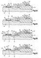
- Fig.1A through 1E depict somewhat diagrammatically the various steps the present invention which are common to all of the embodiments;
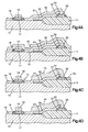
- Fig. 2A shows a step subsequent to the step depicted in Fig. 1E for forming the interconnection according to one embodiment of this invention;
- Fig. 2B is a figure similar to Fig. 2A but showing the resultant structure forming an interconnection between two diffusion regions rather than a diffusion region and a gate region;
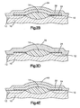
- Figs. 3A through 3C show successively the steps following the step used to produce Fig. 1E for another embodiment of this invention;
- Fig. 3D shows the resulting structure where the embodiment of Figs. 3A through 3C are utilized to connect two diffusion regions rather than a diffusion region and a gate region;
- Figs. 4A through 4D show the steps for practicing another embodiment of this invention following the step used to form Fig. 1 E; and
- Fig. 4E shows the resulting structure of an embodiment similar to Figs. 4A through 4D in which the resulting structure connects two diffusion regions rather than a diffusion and a gate region of the devices.
- Referring now to the drawing and, for the present, to Figs. 1A through 1E, the various initial steps utilized in practicing the present invention for forming integrated circuits, which are common to all of the embodiments, are shown. In depicting these steps, a portion of a single crystal silicon wafer is shown, but this depiction is very schematic and diagrammatic and is simplified to depict the inventive aspects of the present invention.
- Referring now to Fig. 1A, a single crystal sili-
con substrate 10 is shown having a conventional dopedregion 12 formed therein which can be either a "P" or "N" type doping depending upon the particular technology being used. Indeed "P" and "N" dopings can both be used in the same substrate and the particular dopant is not critical for the present invention. A region of recessed oxide (ROX) 14 is shown which is a silicon dioxide material grown on thesilicon substrate 10. Agate electrode 16 of doped polysilicon is shown which is supported on apad 17 of dielectric material such as silicon dioxide. Conventionally, thegate electrode 16 will haveisolation side walls 18 therearound formed of silicon dioxide or some other dielectric material. Asecond pad 20 of doped polysilicon material is shown on therecessed oxide 14. Conventionally, thispad 20 is an extension of another gate and at the location shown is used as its own interconnection line supported on top of therecessed oxide 14. Thepad 20 of doped polysilicon is also surrounded bydielectric side walls 22 again preferably formed of grown silicon dioxide. The processing of a wafer from a silicon substrate to this point to form an integrated circuit is conventional, and is well know to those skilled in the art. - A layer of etch-
stop material 24 is provided over all of the exposed doped silicon regions. In the preferred embodiment, this is a silicon dioxide which is formed on the exposed surfaces of the various regions of doped silicon. However, other etch-stop materials could be used, silicon dioxide being a conventional and convenient material for this purpose. The silicon dioxide etch-stop layer 24 can be formed by either low pressure chemical vapor deposition (LPVCD) or by conventional oxidation processes in an oxygen ambient atmosphere at temperatures above about 750 C. As indicated above, however, other etch-stop materials, such as silicon nitride could be used and applied in a conventional manner. - A layer of
polysilicon 26 is deposited over the entire surface of the wafer structure as shown in Fig. 1 C. This is referred to as intrinsic polysilicon and a preferred technique is by LPCVD Si deposition using silane (SiH4) to form an approximately 1000 angstroms thick layer. - Following the deposition of the
polysilicon layer 26 as shown in Fig. 1 C, thepolysilicon 26 is patterned and etched according to standard photoresist photolithographic technology to reveal the regions of the etch-stop material 24 overlying the underlying doped silicon regions which are to be connected; i.e. the portion of thediffusion zone 12 which may be a source/drain region and a portion of thepad 20 which, as indicated above is an extension of a gate to provide the structure in Fig. 1D. Photoresist and etching techniques are common and well known in the art. The photoresist may be either positive or negative and is imagewise exposed and developed to transfer a pattern to the underlying polysilicon. The polysilicon can be etched in either a dry or wet chemical environment. A typical dry etch gas, having adequate selectivity of sili-con to oxide, is NF3. At this point, it should be noted that one of the important features of the present invention is the provision of the etch-stop layer 24 so that in patterning and etching thepolysilicon layer 26, the underlying dopedregion 12 of thesubstrate 10 is protected and unaffected by the etching process used to pattern thepolysilicon 26. Following the etching of thepolysilicon 26, the revealed portions of the etch-stop layer 24 are removed as shown in Fig. 1E to provide anopening 30 to a portion of the dopedsilicon region 12 and anopening 32 to a portion of the underlying dopedpolysilion pad 20. Buffered hydrofluoric acid (BHF) is used to isotropically remove the oxide etch stop. As indicated above, the steps leading up to and the resulting structure in Fig. 1 E are common to all of the embodiments of the present invention for connecting gate electrodes to source/drain regions. The various embodiments utilize the structure shown in Fig. 1E as the basis for the further steps for the different embodiments, providing the different resulting structures. - Referring now to Fig. 2A, one embodiment of forming the interconnection between the doped sili- con source/
drain region 12 and thepolysilicon region 20 is shown. In this embodiment, the structure of Fig. 1E is used as the starting structure and a layer of tungsten is selectively grown on all of the exposed silicon surfaces, i.e. thesilicon layer 26, the surface of thepad 20 which is exposed and the surface of thepad 16 which is exposed. This layer is designated by thereference character 34. It is important to note that the term selective growth of the tungsten refers to the fact that it grows only on the polysilicon or the doped silicon substrate and not on the oxide. Hence, the oxideside wall barrier 18 around thepad 16 prevents the interconnection of thepad 16 to the source/drain region 12 or thepad 20 by providing an insulating function even though the tungsten does grow on thepad 16 while permitting connection of thepad 20 to source/drain region 12. Tungsten may be selectively grown on silicon substrates using hydrogen (H2) or silane (SiH4) reduction of tungsten hexafloride (WF6) in a LPCVD reactor at temperatures in the range of 250 500 C. Because of this selectivity, thetungsten 34 on thepad 16 does not form a connection or bridge with thetungsten 34 overlying the doped silicon source/drain region 12. Tungsten is a preferred material for this interconnection because of several properties which it possesses. These properties include a high-conductivity, i.e. a low resistivity which allows for good electrical interconnections with the very small line sizes which are required in VLSI semi-conductor technology. Also, tungsten has the characteristic of being able to be selectively grown or deposited on the silicon and not on the silicon dioxide, thereby allowing the isolation of those exposed silicon regions to which connection is not desired. - Fig. 2B is a figure similar to 2A showing the resultant structure of this embodiment of the invention when it is utilized to connect two doped silicon source/drain regions located on opposite sides of the
ROX 14 as opposed to connecting a gate electrode to a source/drain region as depicted in Fig. 2A. It is also to be understood that similar processing steps could be used to connect two gate regions or any other two polysilicon regions. - Referring now to Figs. 3A through 3C, the interconnection of the
pad 20 and a portion of theregion 12 according to another embodiment of the present invention is shown. This embodiment uses a silicide technology for the connection. As shown in Fig. 3A, a layer oftitanium 36 is sputtered (or deposited by some other means) over the entire substrate including being deposited over thepolysilicon layer 26 and the exposed portions ofpads titanium silicide 38. This heating to perform the silicidation can be accomplished by annealing in a nitrogen ambient atmosphere at temperatures between about 650 C and 700 C. Following the forming of thetitanium silicide 38, the titanium which was not formed into a silicide is removed. This is the titanium which was not in contact with the silicon, e.g. that which is on theside wall spacers 18 and on the recessedoxide layer 14 and which remained as titanium metal or was converted to titanium nitride during silicidation. This titanium and/ortitanium nitride 36 can be removed in a conventional way such as by a wet etch in Huang A reagent (H202: NH40H: H20) at about 65 C for about 5-10 minutes with the resulting structure as shown in Fig. 3C. - Fig. 3D depicts a resulting structure for this particular embodiment of the invention when it is used to connect two doped silicon regions separated by recessed oxide. The steps are the same with the resulting structure being the structure shown in Fig. 3D.
- The titanium silicide formed in this process has a very high conductivity (i.e. low resistance) and provides a good interconnection between the source/
drain layer 12 and thepad 20 as shown in Fig. 3C. However, there are certain characteristics of this process that in some instances render it less desirable than the previously described process or the process which will be described subsequently. These factors include the fact that thetitanium 36 which overlies thesilicon 26, and particularly the dopedsilicon layer 12, forms the silicide. The silicide tends to sink into the silicon as it is formed, thus causing a rather steep step between the etch-stop layer 24 and the surface of thesubstrate 10 and also the surface of thepad 20. Thus, care must be taken to assure that there is a good bridging over of this step by the silicide material to insure good electrical contact. - Another embodiment of the invention is shown in Figs. 4A through 4D. For this embodiment also the starting structure is that shown in Fig. 1 E. On top of this structure a layer of
intrinsic silicon 40 is selectively deposited. This layer of intrinsic sili-con 40 is deposited or grown on all exposed silicon surfaces, i.e. on the surface of thesilicon 26, on the surface of the doped source/drain region 12 that is exposed, and on the surface of thegate electrode 16 and on the surface of thepad 20 which is exposed as shown in Fig. 4A. This can be accomplished by selective epitaxial growth (SEG) of Si on precleaned Si surfaces which may be performed in a LPCVD reactor at temperatures between about 800 C and 950 C using dichlorosilane (SiC12H2), or other chlorosilane gasses and HCI gasses. Following this, a layer oftitanium 42 is applied in a manner similar to that as previously described with respect to the embodiment shown in Figs. 3A through 3C. The entire substrate is then heated as previous described to react thetitanium 42 with the underlyingsilicon 40 to form atitanium silicide 44 as shown in Fig. 4C. - The advantage of this particular process over that shown in Figs. 3A through 3C is that there is an additional layer of silicon to afford reactive material for the "step" bridging the etch-
stop material 24 and thus better insure a good connection over this step. Again, as described with respect to Fig. 3C, the remainingunreacted titanium 42 shown in Fig. 4C is removed as previously described resulting in the structure shown in Fig. 4D. - Fig. 4E shows the resulting structure using the technique shown in Figs. 4A through 4D for connecting source/drain regions separated by recessed oxide.
- While several embodiments of the invention have been shown and described, various adaptations and modifications can be made without departing from the scope of the invention as defined in the appended claims.
Claims (10)
Applications Claiming Priority (2)
| Application Number | Priority Date | Filing Date | Title |
|---|---|---|---|
| US54590990A | 1990-06-28 | 1990-06-28 | |
| US545909 | 1990-06-28 |
Publications (2)
| Publication Number | Publication Date |
|---|---|
| EP0463458A1 true EP0463458A1 (en) | 1992-01-02 |
| EP0463458B1 EP0463458B1 (en) | 1997-01-02 |
Family
ID=24178023
Family Applications (1)
| Application Number | Title | Priority Date | Filing Date |
|---|---|---|---|
| EP91109554A Expired - Lifetime EP0463458B1 (en) | 1990-06-28 | 1991-06-11 | Method and structure for interconnecting different polysilicon zones on semiconductor substrates for integrated circuits |
Country Status (5)
| Country | Link |
|---|---|
| US (2) | US5453400A (en) |
| EP (1) | EP0463458B1 (en) |
| JP (1) | JP2757927B2 (en) |
| CA (1) | CA2043172C (en) |
| DE (1) | DE69123884T2 (en) |
Cited By (2)
| Publication number | Priority date | Publication date | Assignee | Title |
|---|---|---|---|---|
| DE4339919A1 (en) * | 1993-11-23 | 1995-05-24 | Siemens Ag | Prodn. of connection surface for silicon@ region |
| DE19521006A1 (en) * | 1994-06-08 | 1995-12-21 | Hyundai Electronics Ind | Semiconductor component and method for its production |
Families Citing this family (19)
| Publication number | Priority date | Publication date | Assignee | Title |
|---|---|---|---|---|
| US5554549A (en) * | 1995-07-03 | 1996-09-10 | Taiwan Semiconductor Manufacturing Company Ltd. | Salicide process for FETs |
| US5629235A (en) * | 1995-07-05 | 1997-05-13 | Winbond Electronics Corporation | Method for forming damage-free buried contact |
| AU6689296A (en) * | 1995-08-03 | 1997-03-05 | Micron Technology, Inc. | Low cost local interconnect process |
| US5869391A (en) | 1996-08-20 | 1999-02-09 | Micron Technology, Inc. | Semiconductor method of making electrical connection between an electrically conductive line and a node location, and integrated circuitry |
| US5956585A (en) * | 1997-02-19 | 1999-09-21 | Winbond Electronics Corporation | Method of forming a self-aligned damage-free buried contact |
| US6060404A (en) * | 1997-09-05 | 2000-05-09 | Advanced Micro Devices, Inc. | In-situ deposition of stop layer and dielectric layer during formation of local interconnects |
| US6060328A (en) | 1997-09-05 | 2000-05-09 | Advanced Micro Devices, Inc. | Methods and arrangements for determining an endpoint for an in-situ local interconnect etching process |
| US5920796A (en) * | 1997-09-05 | 1999-07-06 | Advanced Micro Devices, Inc. | In-situ etch of BARC layer during formation of local interconnects |
| US6114235A (en) * | 1997-09-05 | 2000-09-05 | Advanced Micro Devices, Inc. | Multipurpose cap layer dielectric |
| US6153933A (en) * | 1997-09-05 | 2000-11-28 | Advanced Micro Devices, Inc. | Elimination of residual materials in a multiple-layer interconnect structure |
| DE19822749A1 (en) * | 1998-05-20 | 1999-12-02 | Siemens Ag | Metal-containing layers produced especially for diffusion barriers, contact layers and/or anti-reflection layers in CMOS circuits, DRAM memory chips or embedded DRAM chips |
| US6335294B1 (en) | 1999-04-22 | 2002-01-01 | International Business Machines Corporation | Wet cleans for cobalt disilicide processing |
| US6372668B2 (en) | 2000-01-18 | 2002-04-16 | Advanced Micro Devices, Inc. | Method of forming silicon oxynitride films |
| US6468899B1 (en) * | 2001-06-27 | 2002-10-22 | Agere Systems Guardian Corp. | Contactless local interconnect process utilizing self-aligned silicide |
| FR2828766B1 (en) * | 2001-08-16 | 2004-01-16 | St Microelectronics Sa | INTEGRATED CIRCUIT COMPRISING ACTIVE ELEMENTS AND AT LEAST ONE PASSIVE ELEMENT, IN PARTICULAR DRAM MEMORY CELLS AND MANUFACTURING METHOD |
| US6559043B1 (en) * | 2002-01-11 | 2003-05-06 | Taiwan Semiconductor Manufacturing Company | Method for electrical interconnection employing salicide bridge |
| EP2450945B1 (en) * | 2010-11-08 | 2013-05-29 | Imec | Method for producing a floating gate memory structure |
| CN103730468B (en) * | 2012-10-16 | 2017-12-01 | 中芯国际集成电路制造(上海)有限公司 | Semiconductor structure and forming method thereof, SRAM memory cell, SRAM memory |
| US9634006B2 (en) | 2014-02-28 | 2017-04-25 | International Business Machines Corporation | Third type of metal gate stack for CMOS devices |
Citations (6)
| Publication number | Priority date | Publication date | Assignee | Title |
|---|---|---|---|---|
| EP0068897A2 (en) * | 1981-07-01 | 1983-01-05 | Hitachi, Ltd. | A method of forming an electrode of a semiconductor device |
| EP0085777A2 (en) * | 1982-02-01 | 1983-08-17 | Texas Instruments Incorporated | Fabrication of devices including selective formation of titanium disilicide by direct reaction |
| EP0091775A2 (en) * | 1982-04-08 | 1983-10-19 | Kabushiki Kaisha Toshiba | A method of manufacturing a semiconductor device comprising an interconnection layer |
| EP0097918A1 (en) * | 1982-06-25 | 1984-01-11 | Matsushita Electronics Corporation | Semiconductor device and method of making the same |
| EP0113522A2 (en) * | 1982-11-30 | 1984-07-18 | Fujitsu Limited | The manufacture of semiconductor devices |
| GB2151847A (en) * | 1983-12-23 | 1985-07-24 | Hitachi Ltd | Semiconductor device with metal silicide layer and fabrication process thereof. |
Family Cites Families (30)
| Publication number | Priority date | Publication date | Assignee | Title |
|---|---|---|---|---|
| US4102733A (en) * | 1977-04-29 | 1978-07-25 | International Business Machines Corporation | Two and three mask process for IGFET fabrication |
| JPS5748246A (en) * | 1980-08-13 | 1982-03-19 | Fujitsu Ltd | Manufacture of semiconductor device |
| JPS57192079A (en) * | 1981-05-22 | 1982-11-26 | Hitachi Ltd | Semiconductor device |
| US4476482A (en) * | 1981-05-29 | 1984-10-09 | Texas Instruments Incorporated | Silicide contacts for CMOS devices |
| US4374700A (en) * | 1981-05-29 | 1983-02-22 | Texas Instruments Incorporated | Method of manufacturing silicide contacts for CMOS devices |
| DE3132809A1 (en) * | 1981-08-19 | 1983-03-10 | Siemens AG, 1000 Berlin und 8000 München | METHOD FOR PRODUCING INTEGRATED MOS FIELD EFFECT TRANSISTORS, ESPECIALLY COMPLEMENTARY MOS FIELD EFFECT TRANSISTOR CIRCUITS WITH AN ADDITIONAL CIRCUIT LEVEL CONSTRUCTED FROM METAL SILICIDES |
| JPS58100451A (en) * | 1981-12-10 | 1983-06-15 | Oki Electric Ind Co Ltd | Semiconductor device and manufacture thereof |
| US4463491A (en) * | 1982-04-23 | 1984-08-07 | Gte Laboratories Incorporated | Method of fabricating a monolithic integrated circuit structure |
| JPS59175726A (en) * | 1983-03-25 | 1984-10-04 | Fujitsu Ltd | Manufacture of semiconductor device |
| JPH0638496B2 (en) * | 1983-06-27 | 1994-05-18 | 日本電気株式会社 | Semiconductor device |
| FR2555365B1 (en) * | 1983-11-22 | 1986-08-29 | Efcis | METHOD FOR MANUFACTURING INTEGRATED CIRCUIT WITH TANTALUM SILICIDE CONNECTIONS AND INTEGRATED CIRCUIT PERFORMED ACCORDING TO THIS METHOD |
| US4519126A (en) * | 1983-12-12 | 1985-05-28 | Rca Corporation | Method of fabricating high speed CMOS devices |
| JPS60130155A (en) * | 1983-12-17 | 1985-07-11 | Toshiba Corp | Semiconductor device |
| US4873204A (en) * | 1984-06-15 | 1989-10-10 | Hewlett-Packard Company | Method for making silicide interconnection structures for integrated circuit devices |
| FR2578272B1 (en) * | 1985-03-01 | 1987-05-22 | Centre Nat Rech Scient | PROCESS FOR FORMING A TUNGSTEN SILICIDE LAYER ON A SUBSTRATE, ESPECIALLY USEFUL FOR REALIZING INTERCONNECTION LAYERS OF INTEGRATED CIRCUITS. |
| JPS6220374A (en) * | 1985-07-19 | 1987-01-28 | Hitachi Ltd | Semiconductor integrated circuit device |
| US4745081A (en) * | 1985-10-31 | 1988-05-17 | International Business Machines Corporation | Method of trench filling |
| JPS63227045A (en) * | 1987-03-17 | 1988-09-21 | Matsushita Electric Ind Co Ltd | Mos semiconductor device and manufacture thereof |
| JPS63313855A (en) * | 1987-06-17 | 1988-12-21 | Seiko Epson Corp | Semiconductor device |
| JPS6415753A (en) * | 1987-07-10 | 1989-01-19 | Mitsui Toatsu Chemicals | Electrophotographic dry toner |
| JPS6457523A (en) * | 1987-08-26 | 1989-03-03 | Mitsubishi Metal Corp | Manufacture of working member for superconducting ceramics |
| US4873205A (en) * | 1987-12-21 | 1989-10-10 | International Business Machines Corporation | Method for providing silicide bridge contact between silicon regions separated by a thin dielectric |
| JPH01281755A (en) * | 1988-05-07 | 1989-11-13 | Seiko Epson Corp | Semiconductor device |
| WO1989011732A1 (en) * | 1988-05-24 | 1989-11-30 | Micron Technology, Inc. | Tisi2 local interconnects |
| US5418179A (en) * | 1988-05-31 | 1995-05-23 | Yamaha Corporation | Process of fabricating complementary inverter circuit having multi-level interconnection |
| JPH027531A (en) * | 1988-06-27 | 1990-01-11 | Nec Corp | Manufacture of semiconductor device |
| JPH039524A (en) * | 1989-06-07 | 1991-01-17 | Fujitsu Ltd | Semiconductor device |
| US5294822A (en) * | 1989-07-10 | 1994-03-15 | Texas Instruments Incorporated | Polycide local interconnect method and structure |
| US5223456A (en) * | 1990-05-02 | 1993-06-29 | Quality Semiconductor Inc. | High density local interconnect in an integrated circit using metal silicide |
| US5124280A (en) * | 1991-01-31 | 1992-06-23 | Sgs-Thomson Microelectronics, Inc. | Local interconnect for integrated circuits |
-
1991
- 1991-04-02 JP JP3094895A patent/JP2757927B2/en not_active Expired - Fee Related
- 1991-05-24 CA CA002043172A patent/CA2043172C/en not_active Expired - Fee Related
- 1991-06-11 DE DE69123884T patent/DE69123884T2/en not_active Expired - Fee Related
- 1991-06-11 EP EP91109554A patent/EP0463458B1/en not_active Expired - Lifetime
-
1993
- 1993-01-19 US US08/006,662 patent/US5453400A/en not_active Expired - Fee Related
-
1996
- 1996-08-26 US US08/702,863 patent/US5672901A/en not_active Expired - Fee Related
Patent Citations (6)
| Publication number | Priority date | Publication date | Assignee | Title |
|---|---|---|---|---|
| EP0068897A2 (en) * | 1981-07-01 | 1983-01-05 | Hitachi, Ltd. | A method of forming an electrode of a semiconductor device |
| EP0085777A2 (en) * | 1982-02-01 | 1983-08-17 | Texas Instruments Incorporated | Fabrication of devices including selective formation of titanium disilicide by direct reaction |
| EP0091775A2 (en) * | 1982-04-08 | 1983-10-19 | Kabushiki Kaisha Toshiba | A method of manufacturing a semiconductor device comprising an interconnection layer |
| EP0097918A1 (en) * | 1982-06-25 | 1984-01-11 | Matsushita Electronics Corporation | Semiconductor device and method of making the same |
| EP0113522A2 (en) * | 1982-11-30 | 1984-07-18 | Fujitsu Limited | The manufacture of semiconductor devices |
| GB2151847A (en) * | 1983-12-23 | 1985-07-24 | Hitachi Ltd | Semiconductor device with metal silicide layer and fabrication process thereof. |
Non-Patent Citations (1)
| Title |
|---|
| INTERNATIONAL ELECTRON DEVICES MEETING TECHNICAL DIGEST 11 December 1988, SAN FRANCISCO, CA. pages 450 - 453; V.V. LEE et al.: "A selective CVD Tungsten local interconnect technology" * |
Cited By (5)
| Publication number | Priority date | Publication date | Assignee | Title |
|---|---|---|---|---|
| DE4339919A1 (en) * | 1993-11-23 | 1995-05-24 | Siemens Ag | Prodn. of connection surface for silicon@ region |
| DE4339919C2 (en) * | 1993-11-23 | 1999-03-04 | Siemens Ag | Manufacturing process for a pad made of silicide for a silicon area |
| DE19521006A1 (en) * | 1994-06-08 | 1995-12-21 | Hyundai Electronics Ind | Semiconductor component and method for its production |
| DE19521006C2 (en) * | 1994-06-08 | 2000-02-17 | Hyundai Electronics Ind | Semiconductor component and method for its production |
| US6261882B1 (en) | 1994-06-08 | 2001-07-17 | Hyundai Electronics Industries Co., Ltd. | Method for fabricating a semiconductor device |
Also Published As
| Publication number | Publication date |
|---|---|
| JP2757927B2 (en) | 1998-05-25 |
| CA2043172A1 (en) | 1991-12-29 |
| EP0463458B1 (en) | 1997-01-02 |
| CA2043172C (en) | 1996-04-09 |
| US5672901A (en) | 1997-09-30 |
| DE69123884T2 (en) | 1997-07-17 |
| DE69123884D1 (en) | 1997-02-13 |
| JPH04233230A (en) | 1992-08-21 |
| US5453400A (en) | 1995-09-26 |
Similar Documents
| Publication | Publication Date | Title |
|---|---|---|
| US5672901A (en) | Structure for interconnecting different polysilicon zones on semiconductor substrates for integrated circuits | |
| EP0264692B1 (en) | Method of forming a bridge contact | |
| EP0377137B1 (en) | Method for selective deposition of refractory metals on silicon substrates | |
| US6410427B1 (en) | Metal silicidation methods and methods for using same | |
| US5326722A (en) | Polysilicon contact | |
| US5874353A (en) | Method of forming a self-aligned silicide device | |
| US4855798A (en) | Semiconductor and process of fabrication thereof | |
| US20020068429A1 (en) | Local interconnect structures and methods for making the same | |
| JPH04211134A (en) | Self-aligned contact and interconnection constitution body | |
| US6605533B2 (en) | Process for forming low resistance metal silicide local interconnects | |
| KR930004295B1 (en) | Connecting method of low resistance | |
| US5639678A (en) | Method of making semiconductor device with metal silicide nitride layer and metal silicide | |
| EP0572214B1 (en) | Method for fabricating an interconnect structure in an integrated circuit | |
| KR0158441B1 (en) | Method of manufacturing semiconductor device | |
| US6291890B1 (en) | Semiconductor device having a silicide structure | |
| US6281118B1 (en) | Method of manufacturing semiconductor device | |
| EP0547600A1 (en) | Refractory metal silicide deposition process and apparatus | |
| KR100322886B1 (en) | Method for forming metal contact of a semiconductor device | |
| US6351038B1 (en) | Integrated circuitry | |
| JP3337825B2 (en) | Semiconductor device having internal wiring and method of manufacturing the same | |
| JPH0756866B2 (en) | Method for manufacturing semiconductor integrated circuit device | |
| US6127270A (en) | Methods of forming refractory metal silicide components and methods of restricting silicon surface migration of a silicon structure | |
| JPH01160009A (en) | Manufacture of semiconductor device | |
| KR100431309B1 (en) | Method for forming metal interconnection in semiconductor device | |
| US6953749B2 (en) | Methods of forming refractory metal silicide components and methods of restricting silicon surface migration of a silicon structure |
Legal Events
| Date | Code | Title | Description |
|---|---|---|---|
| PUAI | Public reference made under article 153(3) epc to a published international application that has entered the european phase |
Free format text: ORIGINAL CODE: 0009012 |
|
| AK | Designated contracting states |
Kind code of ref document: A1 Designated state(s): DE FR GB IT |
|
| 17P | Request for examination filed |
Effective date: 19911219 |
|
| 17Q | First examination report despatched |
Effective date: 19921201 |
|
| GRAG | Despatch of communication of intention to grant |
Free format text: ORIGINAL CODE: EPIDOS AGRA |
|
| GRAH | Despatch of communication of intention to grant a patent |
Free format text: ORIGINAL CODE: EPIDOS IGRA |
|
| GRAH | Despatch of communication of intention to grant a patent |
Free format text: ORIGINAL CODE: EPIDOS IGRA |
|
| GRAA | (expected) grant |
Free format text: ORIGINAL CODE: 0009210 |
|
| AK | Designated contracting states |
Kind code of ref document: B1 Designated state(s): DE FR GB IT |
|
| REF | Corresponds to: |
Ref document number: 69123884 Country of ref document: DE Date of ref document: 19970213 |
|
| ITF | It: translation for a ep patent filed |
Owner name: IBM - DR. ALFREDO BRAVI |
|
| ET | Fr: translation filed | ||
| PG25 | Lapsed in a contracting state [announced via postgrant information from national office to epo] |
Ref country code: GB Free format text: LAPSE BECAUSE OF NON-PAYMENT OF DUE FEES Effective date: 19970611 |
|
| PLBE | No opposition filed within time limit |
Free format text: ORIGINAL CODE: 0009261 |
|
| STAA | Information on the status of an ep patent application or granted ep patent |
Free format text: STATUS: NO OPPOSITION FILED WITHIN TIME LIMIT |
|
| 26N | No opposition filed | ||
| GBPC | Gb: european patent ceased through non-payment of renewal fee |
Effective date: 19970611 |
|
| PG25 | Lapsed in a contracting state [announced via postgrant information from national office to epo] |
Ref country code: FR Free format text: LAPSE BECAUSE OF NON-PAYMENT OF DUE FEES Effective date: 19980227 |
|
| REG | Reference to a national code |
Ref country code: FR Ref legal event code: ST |
|
| REG | Reference to a national code |
Ref country code: FR Ref legal event code: ST |
|
| PGFP | Annual fee paid to national office [announced via postgrant information from national office to epo] |
Ref country code: DE Payment date: 20030624 Year of fee payment: 13 |
|
| PG25 | Lapsed in a contracting state [announced via postgrant information from national office to epo] |
Ref country code: DE Free format text: LAPSE BECAUSE OF NON-PAYMENT OF DUE FEES Effective date: 20050101 |
|
| PG25 | Lapsed in a contracting state [announced via postgrant information from national office to epo] |
Ref country code: IT Free format text: LAPSE BECAUSE OF NON-PAYMENT OF DUE FEES;WARNING: LAPSES OF ITALIAN PATENTS WITH EFFECTIVE DATE BEFORE 2007 MAY HAVE OCCURRED AT ANY TIME BEFORE 2007. THE CORRECT EFFECTIVE DATE MAY BE DIFFERENT FROM THE ONE RECORDED. Effective date: 20050611 |