EP0458362A2 - Programmierbares logisches Feld (PLA) mit geringem Leistungsverbrauch und Datenverarbeitungssystem mit diesem PLA - Google Patents
Programmierbares logisches Feld (PLA) mit geringem Leistungsverbrauch und Datenverarbeitungssystem mit diesem PLA Download PDFInfo
- Publication number
- EP0458362A2 EP0458362A2 EP91108485A EP91108485A EP0458362A2 EP 0458362 A2 EP0458362 A2 EP 0458362A2 EP 91108485 A EP91108485 A EP 91108485A EP 91108485 A EP91108485 A EP 91108485A EP 0458362 A2 EP0458362 A2 EP 0458362A2
- Authority
- EP
- European Patent Office
- Prior art keywords
- pla
- control means
- data processing
- transferred
- connection control
- Prior art date
- Legal status (The legal status is an assumption and is not a legal conclusion. Google has not performed a legal analysis and makes no representation as to the accuracy of the status listed.)
- Granted
Links
Images


Classifications
-
- H—ELECTRICITY
- H03—ELECTRONIC CIRCUITRY
- H03K—PULSE TECHNIQUE
- H03K19/00—Logic circuits, i.e. having at least two inputs acting on one output; Inverting circuits
- H03K19/02—Logic circuits, i.e. having at least two inputs acting on one output; Inverting circuits using specified components
- H03K19/173—Logic circuits, i.e. having at least two inputs acting on one output; Inverting circuits using specified components using elementary logic circuits as components
- H03K19/177—Logic circuits, i.e. having at least two inputs acting on one output; Inverting circuits using specified components using elementary logic circuits as components arranged in matrix form
-
- H—ELECTRICITY
- H03—ELECTRONIC CIRCUITRY
- H03K—PULSE TECHNIQUE
- H03K19/00—Logic circuits, i.e. having at least two inputs acting on one output; Inverting circuits
- H03K19/0008—Arrangements for reducing power consumption
- H03K19/0016—Arrangements for reducing power consumption by using a control or a clock signal, e.g. in order to apply power supply
-
- H—ELECTRICITY
- H03—ELECTRONIC CIRCUITRY
- H03K—PULSE TECHNIQUE
- H03K19/00—Logic circuits, i.e. having at least two inputs acting on one output; Inverting circuits
- H03K19/02—Logic circuits, i.e. having at least two inputs acting on one output; Inverting circuits using specified components
- H03K19/173—Logic circuits, i.e. having at least two inputs acting on one output; Inverting circuits using specified components using elementary logic circuits as components
- H03K19/177—Logic circuits, i.e. having at least two inputs acting on one output; Inverting circuits using specified components using elementary logic circuits as components arranged in matrix form
- H03K19/17704—Logic circuits, i.e. having at least two inputs acting on one output; Inverting circuits using specified components using elementary logic circuits as components arranged in matrix form the logic functions being realised by the interconnection of rows and columns
- H03K19/17708—Logic circuits, i.e. having at least two inputs acting on one output; Inverting circuits using specified components using elementary logic circuits as components arranged in matrix form the logic functions being realised by the interconnection of rows and columns using an AND matrix followed by an OR matrix, i.e. programmable logic arrays
- H03K19/17716—Logic circuits, i.e. having at least two inputs acting on one output; Inverting circuits using specified components using elementary logic circuits as components arranged in matrix form the logic functions being realised by the interconnection of rows and columns using an AND matrix followed by an OR matrix, i.e. programmable logic arrays with synchronous operation, i.e. using clock signals, e.g. of I/O or coupling register
- H03K19/1772—Logic circuits, i.e. having at least two inputs acting on one output; Inverting circuits using specified components using elementary logic circuits as components arranged in matrix form the logic functions being realised by the interconnection of rows and columns using an AND matrix followed by an OR matrix, i.e. programmable logic arrays with synchronous operation, i.e. using clock signals, e.g. of I/O or coupling register with synchronous operation of at least one of the logical matrixes
Definitions
- the present invention relates to a low power consumption programmable logic array (PLA) and a data processing system in which the PLA is incorporated.
- PLA programmable logic array
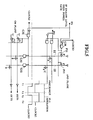
- Fig. 1 is a diagram showing the configuration of a conventional PLA which is frequently used in the prior art.
- This PLA is an asynchronous type or a ratio type.
- a product term line 11 connected to the power source VDD through a load transistor T11 which comprises a P channel conductivity type transistor and is in the ON state at all times is connected to ground through the array transistor T10, when the array transistor T10 enters the ON state.
- the magnitude of the potential of the product term line 11 is determined in accordance with the rate between the ON resistance of the load transistor T11 and that of the array transistor T10.
- the channel conductance of the load transistor T11 is smaller than that of the array transistor T10. Accordingly, the potential of the product term line 11 is switched to low level from high level.
- the array transistor T10 when the input line 10 is at the high level, the array transistor T10 is ON and a current flows continuously to ground through the transistors T10 and T11 which are in the ON state.
- the array transistors other than the array transistor T10 connected to high level input line in the AND array plane are operated similarly.
- an array transistor T12 in the OR array plane remains at the high level and a current flows continuously from the power source VDD to ground through the load transistor T13 and the array transistor T12 which are in the ON state because the product term line 11 is maintained at the high level.
- the array transistors for which the gate terminals are connected to the high level product term lines are operated similarly.
- a problem with the conventional PLA in the prior art is that the current flows continuously from the power source VDD to ground through the array and the load transistors when the PLA is activated.
- Fig. 2 is a block diagram of a data processing system with the conventional PLA.
- the data processing system is operated according to the following procedures:
- instructions written in an machine language stored in the memory 70 are read out by a memory fetch unit 71, then stored in a machine language register 72. At the same time, the instruction fetch unit 72 sets a valid bit register 73a to "1".
- the machine language instruction is transferred to a PLA 74, then decoded and set in the micro instruction register 75. At the same time, the content of the valid bit register 73a are set in a valid bit register 73b.
- An execution unit 76 implements the data processing operation in accordance with the contents of the micro instruction register 75. These units such as the instruction fetch unit 71, the PLA 74, and the execution unit 76 described above are installed in parallel.
- the electric current flows in the conventional PLA when the power source is turned on and no effective output is provided (hereinafter referred to as the unused state).
- the power consumption of the PLA or the data processing system in the situation described above is increased by the steady electrical current flowing therein.
- the power consumption of the PLA is increased when it is in the unused state for a long time.
- no effective output of the PLA 74 can be provided when no machine language instruction is stored in the machine language register 72 and when the content of the valid bit register 73a are zero.
- the power consumption of the PLA is increased because the PLA 74 is in operation when the content of the valid bit register 73a are zero.
- the operation of the PLA 74 has no meaning while the valid bit register 73b is set at 1 and the execution unit 76 is executing.
- the power consumption of the PLA 74 is increased.
- An object of the present invention is to provide a low power consumption programmable logic array (PLA) which is capable of reducing the power consumption while the PLA is in the unused state and a data processing system incorporating the PLA.
- PLA programmable logic array
- the power consumption of the PLA according to the present invention can be reduced.
- PLA described above can be applied to various data processing system.
- Figs. 3 and 4 are configuration diagrams of a PLA as the first and second embodiment according to the present invention.
- the PLA which is a ratio type and an asynchronous type, is incorporated in a LSI system in which a microprocessor as a macro block and a programmable logic device (PLD) are fabricated as independent chips, respectively.
- PLD programmable logic device
- each input line 10 which is represented as one of the input lines in an AND plane, is connected to an output terminal of each AND gate G10 which is represented as one of the AND gates in the AND plane.
- One input terminal of each AND gate is connected to an output terminal of an invert gate (inverter) G12 for which the input terminal is connected to an output terminal of an inverter G11 through which an enable signal is inverted.
- the other input terminal of the AND gate G10 is connected to either an output terminal of an inverter G13 or one of input terminals IN1, IN2, ..., and INn.
- each output line 12 which is represented as one of output lines in an OR plane is connected to the power source VDD through the load transistor T14 comprising a P channel type transistor for which the gate terminal is connected to an output terminal of the inverter G11.
- the enable signal of the high level (H) is provided to an enable terminal EN when the PLA enters the used state.
- One of the input terminals of each AND gate G10 enters the high level, so that either the input signal or the inverted input signal is provided to each input line 10.
- Each load transistor T14 enters the ON state because the output terminal of the inverter G11 is at the low level when the high level enable signal is provided to the enable terminal EN. Accordingly, the electrical power of the power source VDD is provided to each output line 12 in an OR array in the PLA.
- the low level enable signal is provided to the enable terminal EN.
- each AND gate G10 enters the low level, so that the potential of each input line 10 enters the low level regardless of the whether the level of the input signal provided to the input terminals IN1, IN2,..., and INn is at the low level or the high level. Accordingly, all array transistors T10 connected to the input lines 10 enter the inactive state.
- the power consumption P of the PLA with the configuration described above is expressed as follows: where the current flowing in each load transistor in the PLA is Ii, the voltage of the power source VDD is V, i is a positive integer corresponding to each load transistor, and T means (the total unused time for the PLA) / (the total used time for the PLA).
- a load current of 0.2 mA flows in the load transistors when the gate width of the load transistor is 1 ⁇ m.
- the gate capacitance of the array transistors connected to one input line is expressed as follows:
- the electrical power consumption P1 of the input lines is as follows:
- the power consumption of the PLA of the present embodiment according to the invention can be reduced.
- the power consumption of the PLA can be also reduced when the PLA is applied to a component, for example an instruction decoder, in a system logical LSI.
- the T in the formula (1) becomes half of the PLA described above.
- the power consumption P in the PLA becomes as follows:
- the power consumption of the PLA can be reduced by the present invention.
- Fig. 4 is a configuration diagram of a PLA as the second embodiment of the invention.
- the output lines in the OR plane and the product term lines in the AND plane are cut off from the power source VDD when the PLA enter the unused state.
- load transistor T15 in the AND plane and load transistor T16 in the OR plane are connected to an output terminal of an inverter G14 for which the input terminal is connected to the enable terminal EN.
- the inverter G14 inverts the enable signal to provide the inverted enable signal to the gate terminals of the load transistors.
- the enable signal of the low level is provided to the enable terminal EN when the PLA enters the unused state.
- all load transistors in the AND and OR planes enter the inactive state because the output of the inverter G14 is at the high level.
- An electric charge on the product term line 11 flows to ground through the array transistor which enters the active state when at least one array transistor T10 connected to the product term lines 11 enters the active state in accordance with the input signal provided to the input line 10.
- the electric charges on the product term lines 11 cannot flow to ground when all array transistors connected to the product term lines 11 enter the inactive state.
- an electric charge on the output line 12 flows to ground through the array transistor which enters the active state when at least one array transistor enters the active state in the OR plane.
- the electric potential of the output line 12 is maintained at the high level because no electric charge on the output line 12 flows to ground when all array transistors connected to the output line 12 enter the inactive state.
- Fig. 5 is a brief configuration diagram of a precharge type programmable logic array according to the present invention.
- the enable signal and the inverted signal of a clock signal CLOCK1 are provided to the input terminals of the NAND gate G30, then the output of the NAND gate G30 is provided to the gate of the precharge transistor P11 which keeps the product term lines 11 at a predetermined potential level.
- the output of the product term line 11 in the AND plane is provided to the product term lines in the OR plane through the AND gate G32.
- the enable signal and the inverted signal of the clock signal CLOCK2 are provided to the input terminals of the NAND gate G31, then the signal from the NAND gate 31 is provided to one of the input terminals of the AND gate 32.
- the output of the product term line in the AND plane is supplied to the other input terminal of the AND gate G32.
- the phase of the clock signal CLOCK1 differs from that of the clock signal CLOCK2.
- the PLA operates normally (namely, it enters the active state) during the time period between the times t3 and t4 as shown in Fig. 5 when the enable signal EN is in the high level.
- the end timing of the precharge operation in the PLA is detected at the time t3 which is a rising portion of the clock signal CLOCK2.
- the PLA cannot operate (namely, it enters the inactive state) during the time period between the times t1 and t3 as shown in Fig. 5 when the enable signal EN is in the low level.
- the precharge operation for the PLA is continuously executed in the activate state of the PLA.
- the PLA of the present embodiment can also decrease its power consumption while the enable signal EN is in the low stete.
- the preferred timing period between the time t2 and the time t3 may be determined in accordance with the kind of the PLA.
- Fig. 6 is a block diagram of the third embodiment in which the PLA of the first and second embodiments is used as an instruction decoder in a microprocessor.
- an instruction fetch unit 21 provides a machine language instruction to a machine language register 22 and sets a valid bit indicating which the machine language instruction stored in the machine language register 22 is effective at the high level (H) in a valid bit register 23a when the machine language instruction is fetched by the instruction fetch unit 21 from an instruction cache memory 20.
- the machine language instruction stored in the register 22 is provided to the PLA 24 which acts as the instruction decoder and the valid bit in the valid bit register 23a is transferred to the enable terminal EN as the enable signal at the next cycle
- the PLA 24 decodes the machine language instruction transferred from the machine language register 22. Then, the resultant machine language instruction decoded by the decoder 24 is transferred to the first address in a microprogram memory.
- the valid bit stored in the valid bit register 23a is used as the enable signal for the PLA 24.
- a high level valid bit indicating that the operation of the PLA 24 has been completed normally is set in a valid bit register 23b.
- the low level valid bit (L) indicating that the content of the machine language register 22 are meaningless, is set in the valid bit register 23a in case of an error by the instruction fetch unit 21 or when no machine language instruction is transferred to the machine language instruction 22.
- the PLA enters the unused state because the enable signal in the valid bit is at the low level.
- the power consumption of the PLA according to the present invention can be easily reduced by using the enable signal as the contents of the valid bit register.
- PLAs of the first and second embodiments are incorporated in a system 100 as programmable logic devices (PLDs) fabricated on one chip.
- PLDs programmable logic devices
- Fig. 7 is a block diagram of the system with the PLDs provided together with a CPU 30 and other components on one chip.
- the CPU 30 uses an address signal of 32 bits. There are, for example, memory regions, and I/O regions in an address space of the CPU 30.
- the PLD 31 decodes highest 2 bit address signals transferred from the CPU 30, then provides selecting signal to select the regions to the PLD 32, 33, and the like.
- only the selecting signal corresponding to the selected memory region is at the high level, and is then transferred to the enable terminal EN of the PLD which controls the selected memory region.
- the PLD 32 is switched to the active state by the enable signal of the high level, then decodes a two bit address signal following the highest two bit address signal to control four memories such as a DRAM 34a, a ROM 34b, a SRAM1 34c, and a SRAM2 in the region.
- the enable signal indicating whether the regions corresponding to the PLD are selected or not is provided to the enable terminal of the PLD to control the operation of the regions.
- the power consumption of the PLD can be, therefore, reduced by the present invention.
- Fig. 8 is a block diagram of a data processing system based on a pipeline system as a fifth embodiment, in which the PLAs according to the first and second embodiments are used.
- An inverter 69 inverts the contents of the valid bit register 73b, then provides this data to an OR gate 68.
- the OR gate 68 takes the logical sum of the output of the inverter 69 and a final signal 60 indicating the end of the operation of the execution unit 76, then provides the result to an AND gate 67.
- the AND gate takes the logical product of the content of the valid bit register 73a and the output of the OR gate 68, then provides the result to the PLA 65.
- the PLA 65 operates only when a PLA activation signal 61 is at the high level (H). Conversly, the PLA 65 does not operated when the PLA activation signal 61 is at the low level (H).
- the operation of the PLA 65 may be stopped when the content of the valid bit register 73a are at the low level (when the effective data is not stored in the machine language instruction register 72).
- the AND gate 67 provides a low level enable signal to the PLA 65 when the content of the valid bit register 73a are at the low level.
- the content of the micro instruction register 75 should be maintained until the end operation of the execution unit 76 while the execution unit 76 is operating even if the effective contents are stored in the machine language instruction register 75.
- the OR gate 68 outputs a low level signal (L) to the AND gate 67 to halt the operation of the PLA 65 when the content of the valid bit register 73b are at the high level (H) and the end signal indicating the end operation of the execution unit 76 are at the low level (L).
- the PLA activation signal 61 for the PLA 67 enters the high level (H) to execute the PLA 67 when the contents of the valid bit register 73b are at the low level or the end signal 60 is at the high level.
- the dead operation of the PLA 65 is suppressed by using the PLA activation signal 61 which is capable of controlling the operation of the PLA 65, so that the power consumption of the PLA 65 can be reduced.
- a detecting means to detect whether the PLA enters the active state or the inactive state by the present invention is easily provided, as described in the third, fourth, and fifth embodiments as shown in Figs. 6, 7, and 8.
- the selecting signal as the enable signal described above in these embodiments in detail is readily selected.
- the concept of the present invention is not limited by the embodiments described above, but for example, can be applied to a RAM or an ROM and the other components of a data processing system.
Landscapes
- Physics & Mathematics (AREA)
- Mathematical Physics (AREA)
- Engineering & Computer Science (AREA)
- Computer Hardware Design (AREA)
- Computing Systems (AREA)
- General Engineering & Computer Science (AREA)
- Logic Circuits (AREA)
- Power Sources (AREA)
- Executing Machine-Instructions (AREA)
Applications Claiming Priority (4)
| Application Number | Priority Date | Filing Date | Title |
|---|---|---|---|
| JP132498/90 | 1990-05-24 | ||
| JP13249890 | 1990-05-24 | ||
| JP3097579A JP2544027B2 (ja) | 1990-05-24 | 1991-04-26 | 低消費電力型プログラマブルロジックアレイおよびそれを用いた情報処理装置 |
| JP97579/91 | 1991-04-26 |
Publications (3)
| Publication Number | Publication Date |
|---|---|
| EP0458362A2 true EP0458362A2 (de) | 1991-11-27 |
| EP0458362A3 EP0458362A3 (en) | 1992-08-19 |
| EP0458362B1 EP0458362B1 (de) | 1998-01-28 |
Family
ID=26438746
Family Applications (1)
| Application Number | Title | Priority Date | Filing Date |
|---|---|---|---|
| EP91108485A Expired - Lifetime EP0458362B1 (de) | 1990-05-24 | 1991-05-24 | Programmierbares logisches Feld (PLA) vom Vorladungstype mit geringem Leistungsverbrauch |
Country Status (5)
| Country | Link |
|---|---|
| US (1) | US5634061A (de) |
| EP (1) | EP0458362B1 (de) |
| JP (1) | JP2544027B2 (de) |
| KR (1) | KR910021033A (de) |
| DE (1) | DE69128812T2 (de) |
Cited By (1)
| Publication number | Priority date | Publication date | Assignee | Title |
|---|---|---|---|---|
| EP0645700A3 (de) * | 1993-09-29 | 1996-05-01 | Toshiba Kk | Programmierbare logische Anordnung. |
Families Citing this family (3)
| Publication number | Priority date | Publication date | Assignee | Title |
|---|---|---|---|---|
| GB2344303B (en) * | 1997-09-01 | 2002-12-11 | United Microelectronics Corp | Chemical-mechanical polishing machine and retainer ring thereof |
| US6125440A (en) * | 1998-05-21 | 2000-09-26 | Tellabs Operations, Inc. | Storing executing instruction sequence for re-execution upon backward branch to reduce power consuming memory fetch |
| JP2003045189A (ja) * | 2001-07-31 | 2003-02-14 | Fujitsu Ltd | 半導体メモリ |
Family Cites Families (22)
| Publication number | Priority date | Publication date | Assignee | Title |
|---|---|---|---|---|
| US3599182A (en) * | 1969-01-15 | 1971-08-10 | Ibm | Means for reducing power consumption in a memory device |
| US3987287A (en) * | 1974-12-30 | 1976-10-19 | International Business Machines Corporation | High density logic array |
| DE2713648A1 (de) * | 1976-03-26 | 1977-10-06 | Tokyo Shibaura Electric Co | Stromzufuhr-steuervorrichtung fuer speichervorrichtungen |
| JPS52137229A (en) * | 1976-05-12 | 1977-11-16 | Hitachi Ltd | Programmable logic array |
| US4233667A (en) * | 1978-10-23 | 1980-11-11 | International Business Machines Corporation | Demand powered programmable logic array |
| US4399516A (en) * | 1981-02-10 | 1983-08-16 | Bell Telephone Laboratories, Incorporated | Stored-program control machine |
| US4598383A (en) * | 1981-12-28 | 1986-07-01 | Texas Instruments Incorporated | Combination of a data processor with a switch means |
| US4514650A (en) * | 1982-10-25 | 1985-04-30 | Burroughs Corporation | Low power small area PLA |
| JPS5999823A (ja) * | 1982-11-29 | 1984-06-08 | Nec Corp | ロジツクアレイ |
| US4645953A (en) * | 1984-07-03 | 1987-02-24 | Monolithic Memories, Inc. | Current source which saves power in programmable logic array circuitry |
| JPS61101124A (ja) * | 1984-10-24 | 1986-05-20 | Hitachi Micro Comput Eng Ltd | 半導体集積回路装置 |
| US4775927A (en) * | 1984-10-31 | 1988-10-04 | International Business Machines Corporation | Processor including fetch operation for branch instruction with control tag |
| JP2594928B2 (ja) * | 1986-10-29 | 1997-03-26 | 川崎製鉄株式会社 | ストリツプコイルの層間スリツプ検出方法 |
| JPS63177165A (ja) * | 1987-01-19 | 1988-07-21 | Canon Inc | 現像装置 |
| JP2544732B2 (ja) * | 1987-01-19 | 1996-10-16 | 沖電気工業株式会社 | 半導体論理回路 |
| US4831285A (en) * | 1988-01-19 | 1989-05-16 | National Semiconductor Corporation | Self precharging static programmable logic array |
| DE3801587A1 (de) * | 1988-01-21 | 1989-08-03 | Hoechst Ag | Neue aminosaeureglyceride, verfahren zu ihrer herstellung, sie enthaltende arzneimittel und deren verwendung |
| US4857767A (en) * | 1988-03-03 | 1989-08-15 | Dallas Semiconductor Corporation | High-density low-power circuit for sustaining a precharge level |
| JPH01260942A (ja) * | 1988-04-11 | 1989-10-18 | Fujitsu Ltd | クロスコネクト装置 |
| JP2547436B2 (ja) * | 1988-04-11 | 1996-10-23 | 富士通株式会社 | Pla制御方式 |
| US4968900A (en) * | 1989-07-31 | 1990-11-06 | Harris Corporation | Programmable speed/power arrangement for integrated devices having logic matrices |
| US5276824A (en) * | 1990-01-08 | 1994-01-04 | Motorola, Inc. | Data processor having a multi-stage instruction pipe and selection logic responsive to an instruction decoder for selecting one stage of the instruction pipe |
-
1991
- 1991-04-26 JP JP3097579A patent/JP2544027B2/ja not_active Expired - Lifetime
- 1991-05-23 KR KR1019910008314A patent/KR910021033A/ko not_active Ceased
- 1991-05-24 DE DE69128812T patent/DE69128812T2/de not_active Expired - Lifetime
- 1991-05-24 EP EP91108485A patent/EP0458362B1/de not_active Expired - Lifetime
-
1994
- 1994-04-25 US US08/232,405 patent/US5634061A/en not_active Expired - Lifetime
Cited By (2)
| Publication number | Priority date | Publication date | Assignee | Title |
|---|---|---|---|---|
| EP0645700A3 (de) * | 1993-09-29 | 1996-05-01 | Toshiba Kk | Programmierbare logische Anordnung. |
| US5672984A (en) * | 1993-09-29 | 1997-09-30 | Kabushiki Kaisha Toshiba | Programmable logic array having power-saving banks |
Also Published As
| Publication number | Publication date |
|---|---|
| DE69128812D1 (de) | 1998-03-05 |
| EP0458362B1 (de) | 1998-01-28 |
| JP2544027B2 (ja) | 1996-10-16 |
| DE69128812T2 (de) | 1998-06-10 |
| KR910021033A (ko) | 1991-12-20 |
| US5634061A (en) | 1997-05-27 |
| EP0458362A3 (en) | 1992-08-19 |
| JPH04227327A (ja) | 1992-08-17 |
Similar Documents
| Publication | Publication Date | Title |
|---|---|---|
| US7123541B2 (en) | Memory with address management | |
| US6914845B2 (en) | Semiconductor device saving data in non-volatile manner during standby | |
| JP3754593B2 (ja) | データビットを記憶するメモリーセルを有する集積回路および集積回路において書き込みデータビットをメモリーセルに書き込む方法 | |
| KR930008577B1 (ko) | 반도체 메모리장치 | |
| US6339343B1 (en) | Data I/O buffer control circuit | |
| KR100323158B1 (ko) | 다중포트메모리셀을구현하는데이터처리시스템및그구현방법 | |
| US5625302A (en) | Address buffer for synchronous system | |
| EP0458362A2 (de) | Programmierbares logisches Feld (PLA) mit geringem Leistungsverbrauch und Datenverarbeitungssystem mit diesem PLA | |
| US6414520B1 (en) | Universal CMOS single input, low swing sense amplifier without reference voltage | |
| KR100665408B1 (ko) | 반도체 메모리 장치의 차동 증폭기 제어회로 | |
| US6084455A (en) | High-speed CMOS latch | |
| US6628552B1 (en) | Self-configuring input buffer on flash memories | |
| US20040085800A1 (en) | Semiconductor integrated circuit device | |
| US5907519A (en) | Write driver circuit with write-per-bit data masking function | |
| KR100278954B1 (ko) | 다중포트 메모리 셀을 구현하는 데이타 처리 시스템 및 그 구현방법 | |
| EP0352745A2 (de) | Mikroprozessor | |
| US5533196A (en) | Method and apparatus for testing for a sufficient write voltage level during power up of a SRAM array | |
| KR960003402B1 (ko) | 반도체 기억 장치 | |
| US4514802A (en) | Integrated program counter memory management register and incrementer | |
| JPH1069336A (ja) | 集積回路 | |
| JP2000173283A (ja) | 半導体記憶装置及びデータ処理装置 | |
| US5179678A (en) | Address/control signal input circuit for a cache controller which clamps the address/control signals to predetermined logic level clamp signal is received | |
| US6239647B1 (en) | Decoder circuit and decoding method of the same | |
| KR100228357B1 (ko) | 메모리의 데이터 입출력 장치 | |
| KR100234368B1 (ko) | 병렬 비트 테스트 회로 |
Legal Events
| Date | Code | Title | Description |
|---|---|---|---|
| PUAI | Public reference made under article 153(3) epc to a published international application that has entered the european phase |
Free format text: ORIGINAL CODE: 0009012 |
|
| 17P | Request for examination filed |
Effective date: 19910524 |
|
| AK | Designated contracting states |
Kind code of ref document: A2 Designated state(s): DE FR GB |
|
| PUAL | Search report despatched |
Free format text: ORIGINAL CODE: 0009013 |
|
| AK | Designated contracting states |
Kind code of ref document: A3 Designated state(s): DE FR GB |
|
| 17Q | First examination report despatched |
Effective date: 19951023 |
|
| GRAG | Despatch of communication of intention to grant |
Free format text: ORIGINAL CODE: EPIDOS AGRA |
|
| GRAG | Despatch of communication of intention to grant |
Free format text: ORIGINAL CODE: EPIDOS AGRA |
|
| GRAH | Despatch of communication of intention to grant a patent |
Free format text: ORIGINAL CODE: EPIDOS IGRA |
|
| GRAH | Despatch of communication of intention to grant a patent |
Free format text: ORIGINAL CODE: EPIDOS IGRA |
|
| GRAA | (expected) grant |
Free format text: ORIGINAL CODE: 0009210 |
|
| AK | Designated contracting states |
Kind code of ref document: B1 Designated state(s): DE FR GB |
|
| REF | Corresponds to: |
Ref document number: 69128812 Country of ref document: DE Date of ref document: 19980305 |
|
| ET | Fr: translation filed | ||
| REG | Reference to a national code |
Ref country code: GB Ref legal event code: 746 Effective date: 19981012 |
|
| PLBE | No opposition filed within time limit |
Free format text: ORIGINAL CODE: 0009261 |
|
| STAA | Information on the status of an ep patent application or granted ep patent |
Free format text: STATUS: NO OPPOSITION FILED WITHIN TIME LIMIT |
|
| 26N | No opposition filed | ||
| REG | Reference to a national code |
Ref country code: FR Ref legal event code: D6 |
|
| REG | Reference to a national code |
Ref country code: GB Ref legal event code: IF02 |
|
| REG | Reference to a national code |
Ref country code: FR Ref legal event code: ST Effective date: 20090119 |
|
| REG | Reference to a national code |
Ref country code: FR Ref legal event code: D3 |
|
| PGFP | Annual fee paid to national office [announced via postgrant information from national office to epo] |
Ref country code: GB Payment date: 20100329 Year of fee payment: 20 |
|
| PGFP | Annual fee paid to national office [announced via postgrant information from national office to epo] |
Ref country code: FR Payment date: 20100525 Year of fee payment: 20 |
|
| PGFP | Annual fee paid to national office [announced via postgrant information from national office to epo] |
Ref country code: DE Payment date: 20100519 Year of fee payment: 20 |
|
| REG | Reference to a national code |
Ref country code: DE Ref legal event code: R071 Ref document number: 69128812 Country of ref document: DE |
|
| REG | Reference to a national code |
Ref country code: GB Ref legal event code: PE20 Expiry date: 20110523 |
|
| PG25 | Lapsed in a contracting state [announced via postgrant information from national office to epo] |
Ref country code: GB Free format text: LAPSE BECAUSE OF EXPIRATION OF PROTECTION Effective date: 20110523 |
|
| PG25 | Lapsed in a contracting state [announced via postgrant information from national office to epo] |
Ref country code: DE Free format text: LAPSE BECAUSE OF EXPIRATION OF PROTECTION Effective date: 20110525 |