EP0450163A1 - Dispositif pour revêtir un substrat avec les matériaux, par exemple avec les métaux - Google Patents
Dispositif pour revêtir un substrat avec les matériaux, par exemple avec les métaux Download PDFInfo
- Publication number
- EP0450163A1 EP0450163A1 EP90123512A EP90123512A EP0450163A1 EP 0450163 A1 EP0450163 A1 EP 0450163A1 EP 90123512 A EP90123512 A EP 90123512A EP 90123512 A EP90123512 A EP 90123512A EP 0450163 A1 EP0450163 A1 EP 0450163A1
- Authority
- EP
- European Patent Office
- Prior art keywords
- substrate
- targets
- coating
- materials
- atomized
- Prior art date
- Legal status (The legal status is an assumption and is not a legal conclusion. Google has not performed a legal analysis and makes no representation as to the accuracy of the status listed.)
- Ceased
Links
Images
Classifications
-
- C—CHEMISTRY; METALLURGY
- C23—COATING METALLIC MATERIAL; COATING MATERIAL WITH METALLIC MATERIAL; CHEMICAL SURFACE TREATMENT; DIFFUSION TREATMENT OF METALLIC MATERIAL; COATING BY VACUUM EVAPORATION, BY SPUTTERING, BY ION IMPLANTATION OR BY CHEMICAL VAPOUR DEPOSITION, IN GENERAL; INHIBITING CORROSION OF METALLIC MATERIAL OR INCRUSTATION IN GENERAL
- C23C—COATING METALLIC MATERIAL; COATING MATERIAL WITH METALLIC MATERIAL; SURFACE TREATMENT OF METALLIC MATERIAL BY DIFFUSION INTO THE SURFACE, BY CHEMICAL CONVERSION OR SUBSTITUTION; COATING BY VACUUM EVAPORATION, BY SPUTTERING, BY ION IMPLANTATION OR BY CHEMICAL VAPOUR DEPOSITION, IN GENERAL
- C23C14/00—Coating by vacuum evaporation, by sputtering or by ion implantation of the coating forming material
- C23C14/22—Coating by vacuum evaporation, by sputtering or by ion implantation of the coating forming material characterised by the process of coating
- C23C14/225—Oblique incidence of vaporised material on substrate
-
- C—CHEMISTRY; METALLURGY
- C23—COATING METALLIC MATERIAL; COATING MATERIAL WITH METALLIC MATERIAL; CHEMICAL SURFACE TREATMENT; DIFFUSION TREATMENT OF METALLIC MATERIAL; COATING BY VACUUM EVAPORATION, BY SPUTTERING, BY ION IMPLANTATION OR BY CHEMICAL VAPOUR DEPOSITION, IN GENERAL; INHIBITING CORROSION OF METALLIC MATERIAL OR INCRUSTATION IN GENERAL
- C23C—COATING METALLIC MATERIAL; COATING MATERIAL WITH METALLIC MATERIAL; SURFACE TREATMENT OF METALLIC MATERIAL BY DIFFUSION INTO THE SURFACE, BY CHEMICAL CONVERSION OR SUBSTITUTION; COATING BY VACUUM EVAPORATION, BY SPUTTERING, BY ION IMPLANTATION OR BY CHEMICAL VAPOUR DEPOSITION, IN GENERAL
- C23C14/00—Coating by vacuum evaporation, by sputtering or by ion implantation of the coating forming material
- C23C14/22—Coating by vacuum evaporation, by sputtering or by ion implantation of the coating forming material characterised by the process of coating
- C23C14/34—Sputtering
- C23C14/35—Sputtering by application of a magnetic field, e.g. magnetron sputtering
- C23C14/352—Sputtering by application of a magnetic field, e.g. magnetron sputtering using more than one target
-
- H—ELECTRICITY
- H01—ELECTRIC ELEMENTS
- H01J—ELECTRIC DISCHARGE TUBES OR DISCHARGE LAMPS
- H01J37/00—Discharge tubes with provision for introducing objects or material to be exposed to the discharge, e.g. for the purpose of examination or processing thereof
- H01J37/32—Gas-filled discharge tubes
- H01J37/34—Gas-filled discharge tubes operating with cathodic sputtering
- H01J37/3402—Gas-filled discharge tubes operating with cathodic sputtering using supplementary magnetic fields
- H01J37/3405—Magnetron sputtering
Definitions
- the invention relates to a device for coating a substrate with materials, for example with metals, consisting of one or more current sources which are connected to electrodes arranged in an evacuable coating chamber, which are electrically connected to targets which are atomized and whose atomized particles are themselves deposit on the substrate, a process gas being able to be introduced into the coating chamber.
- Cathode sputtering devices with several targets are known, which are arranged side by side and are formed from different materials to be sputtered (DE-OS 26 36 293, DE-OS 29 32 483; DD-PS 111 409, DE-OS 1 790 178).
- the present invention has for its object to provide a device which is suitable to significantly improve the quality of sputtered layers without conventional or existing devices or systems are unsuitable for this or without significant or costly conversions or Changes need to be made.
- This object is achieved in that the targets made of one or more materials to be atomized are each held at an angle to the plane of the substrate, the main directions of migration of the particle streams of the targets aligned on the substrate intersecting.
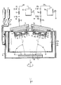
- the invention allows a wide variety of design options; one of them is shown schematically in the attached drawing, which shows a sputtering system with two targets for DC sputtering.
- the drawing shows a substrate 1 which is to be provided with a thin layer 2.
- This Substrate 1 is opposite two targets 3, 3a that are to be atomized.
- the targets 3, 3a are each connected via a section U-shaped element 4, 4a to an electrode 5, 5a, each of which stems from a yoke 6, 6a which has three permanent magnets between it and the element 4, 4a 7, 8, 9 or 7a, 8a, 9a.
- This magnetic field compresses the plasma in front of the target 3 or 3a, so that it has its greatest density where the magnetic fields have the maximum of their circular arc.
- the ions in the plasma are accelerated by electrical fields which build up on the basis of a DC voltage which is indicated by DC sources 10, 10a.
- These direct current sources 10, 10a are each connected with their negative poles to the electrodes 5 and 5a via two inductors 11, 12 and 11a, 12a.
- the electric field is perpendicular to the surface of the assigned target 3 or 3a and accelerates the positive ions of the plasma in the direction of this target.
- more or fewer atoms or particles are knocked out of the target 3 or 3a, in particular from the areas 13, 14 or 13a, 14a, where the magnetic fields have their maxima.
- the atomized atoms or particles migrate in the direction of the substrate 1, where they are deposited as a thin layer 2, specifically in the direction of the axes or arrows l, l 'shown in dashed lines.
- a process computer can be provided to control the arrangement shown, which processes measurement data and issues control commands. For example, the values of the measured partial pressure in the process chamber 15 can be fed to this process computer. Based on this and other data, it can regulate the gas flow via the valves 18, 19 and adjust the voltage at the cathodes 5, 5a, for example.
- the process computer is also able to regulate all other variables, for example cathode current and magnetic field strength. Since such process computers are known, a description of their structure is omitted.
- the individual targets 3, 3a or their electrodes 5, 5a are mounted on annular holding parts or holding collars 31, 31a, so that their flat target surfaces f, f 'are in a tilted position relative to the plane of the substrate 1.
- These retaining collars 31, 31a are cylindrical rings, one end face of which forms an inclined plane (i.e. the upper end face of which is oblique to the longitudinal axis of the respective cylindrical ring).
- the flow of the particles to be sputtered or the axis of symmetry of the sputter cloud in the direction of the substrate is denoted in the drawing by 1 and 1 ', respectively.
- intersection S can be shifted or the angles ⁇ , ⁇ ', ... can be adapted to the sputtering conditions.
Landscapes
- Chemical & Material Sciences (AREA)
- Engineering & Computer Science (AREA)
- Chemical Kinetics & Catalysis (AREA)
- Materials Engineering (AREA)
- Mechanical Engineering (AREA)
- Metallurgy (AREA)
- Organic Chemistry (AREA)
- Physics & Mathematics (AREA)
- Plasma & Fusion (AREA)
- Analytical Chemistry (AREA)
- Physical Vapour Deposition (AREA)
Applications Claiming Priority (2)
| Application Number | Priority Date | Filing Date | Title |
|---|---|---|---|
| DE4010495A DE4010495C2 (de) | 1990-03-31 | 1990-03-31 | Vorrichtung zum Beschichten eines Substrats mit Werkstoffen, beispielweise mit Metallen |
| DE4010495 | 1990-03-31 |
Publications (1)
| Publication Number | Publication Date |
|---|---|
| EP0450163A1 true EP0450163A1 (fr) | 1991-10-09 |
Family
ID=6403540
Family Applications (1)
| Application Number | Title | Priority Date | Filing Date |
|---|---|---|---|
| EP90123512A Ceased EP0450163A1 (fr) | 1990-03-31 | 1990-12-07 | Dispositif pour revêtir un substrat avec les matériaux, par exemple avec les métaux |
Country Status (4)
| Country | Link |
|---|---|
| EP (1) | EP0450163A1 (fr) |
| JP (1) | JPH04228564A (fr) |
| KR (1) | KR910016960A (fr) |
| DE (1) | DE4010495C2 (fr) |
Cited By (8)
| Publication number | Priority date | Publication date | Assignee | Title |
|---|---|---|---|---|
| EP0558797A1 (fr) * | 1992-01-29 | 1993-09-08 | Leybold Aktiengesellschaft | Dispositif de pulvérisation cathodique |
| EP0608478A2 (fr) * | 1992-01-29 | 1994-08-03 | Leybold Aktiengesellschaft | Dispositif de pulvérisation cathodique |
| WO1997041587A1 (fr) * | 1996-04-29 | 1997-11-06 | Von Ardenne Anlagentechnik Gmbh | Installation a pulverisation cathodique a deux magnetrons longitudinaux |
| US6264804B1 (en) | 2000-04-12 | 2001-07-24 | Ske Technology Corp. | System and method for handling and masking a substrate in a sputter deposition system |
| EP1293586A2 (fr) * | 2001-09-13 | 2003-03-19 | Fraunhofer-Gesellschaft zur Förderung der angewandten Forschung e.V. | Dispositif pour le revêtement de substrats à surface courbe par pulvérisation avec un magnétron pulsé |
| WO2010125002A1 (fr) * | 2009-04-27 | 2010-11-04 | Oc Oerlikon Balzers Ag | Pulvérisation cathodique réactive avec de multiples sources de pulvérisation cathodique |
| US8168049B2 (en) * | 2008-05-20 | 2012-05-01 | Canon Anelva Corporation | Sputtering apparatus and method of manufacturing solar battery and image display device by using the same |
| CN111445489A (zh) * | 2019-11-18 | 2020-07-24 | 北京邮电大学 | 一种离子束入射角度确定方法及装置 |
Families Citing this family (15)
| Publication number | Priority date | Publication date | Assignee | Title |
|---|---|---|---|---|
| DE4202425C2 (de) * | 1992-01-29 | 1997-07-17 | Leybold Ag | Verfahren und Vorrichtung zum Beschichten eines Substrats, insbesondere mit elektrisch nichtleitenden Schichten |
| DE4419167B4 (de) * | 1994-06-01 | 2004-09-02 | Leybold Optics Gmbh | Vorrichtung zum Beschichten eines Substrates |
| DE4420951C2 (de) * | 1994-06-16 | 1998-01-22 | Leybold Ag | Einrichtung zum Erfassen von Mikroüberschlägen in Zerstäubungsanlagen |
| DE4441206C2 (de) * | 1994-11-19 | 1996-09-26 | Leybold Ag | Einrichtung für die Unterdrückung von Überschlägen in Kathoden-Zerstäubungseinrichtungen |
| DE19501804A1 (de) | 1995-01-21 | 1996-07-25 | Leybold Ag | Vorrichtung zur Beschichtung von Substraten |
| DE19506513C2 (de) * | 1995-02-24 | 1996-12-05 | Fraunhofer Ges Forschung | Einrichtung zur reaktiven Beschichtung |
| DE19508406A1 (de) * | 1995-03-09 | 1996-09-12 | Leybold Ag | Kathodenanordnung für eine Vorrichtung zum Zerstäuben eines Target-Paares |
| DE19508405A1 (de) * | 1995-03-09 | 1996-09-12 | Leybold Ag | Kathodenanordnung für eine Vorrichtung zum Zerstäuben von einem Target-Paar |
| US5683560A (en) * | 1995-07-08 | 1997-11-04 | Balzers Und Leybold Deutschland Holding Ag | Cathode assembly |
| KR100329630B1 (ko) * | 1998-06-08 | 2002-08-21 | 한전건 | 고속전도성세라믹/금속복합재료코팅방법 |
| DE10145201C1 (de) * | 2001-09-13 | 2002-11-21 | Fraunhofer Ges Forschung | Einrichtung zum Beschichten von Substraten mit gekrümmter Oberfläche durch Pulsmagnetron-Zerstäuben |
| JP4755475B2 (ja) * | 2005-10-06 | 2011-08-24 | 株式会社昭和真空 | スパッタ装置 |
| KR20120044050A (ko) * | 2010-10-27 | 2012-05-07 | 주식회사 에이스테크놀로지 | Rf 장비 도금 방법 및 이에 사용되는 스퍼터링 장치 |
| EP3868917A1 (fr) | 2015-06-16 | 2021-08-25 | Schneider GmbH & Co. KG | Dispositif, procédé et utilisation de revêtement des lentilles |
| DE102016125273A1 (de) | 2016-12-14 | 2018-06-14 | Schneider Gmbh & Co. Kg | Anlage, Verfahren und Träger zur Beschichtung von Brillengläsern |
Citations (3)
| Publication number | Priority date | Publication date | Assignee | Title |
|---|---|---|---|---|
| DE2913724A1 (de) * | 1978-04-07 | 1979-10-11 | Varian Associates | Spruehbeschichtungssystem |
| DE3409342A1 (de) * | 1983-03-16 | 1984-09-20 | Satis Vacuum AG, Zürich | Verfahren und einrichtung zur herstellung optischer substrate mit reversiblen photochromischen eigenschaften |
| EP0347567A2 (fr) * | 1988-06-23 | 1989-12-27 | Leybold Aktiengesellschaft | Dispositif de revêtement d'un diélectrique sur un substrat |
Family Cites Families (5)
| Publication number | Priority date | Publication date | Assignee | Title |
|---|---|---|---|---|
| DE1790178A1 (de) * | 1967-10-11 | 1972-01-20 | Varian Associates | Kathoden-Zerstaeubungsvorrichtung |
| DD111409A1 (fr) * | 1974-05-02 | 1975-02-12 | ||
| DE2636293A1 (de) * | 1976-08-12 | 1978-02-16 | Leybold Heraeus Gmbh & Co Kg | Katodenzerstaeubungsvorrichtung |
| DE2932483A1 (de) * | 1979-08-10 | 1981-04-02 | Leybold-Heraeus GmbH, 5000 Köln | Testglashalter mit einer drehbaren platine und mehreren ausnehmungen fuer testglaeser |
| US4595482A (en) * | 1984-05-17 | 1986-06-17 | Varian Associates, Inc. | Apparatus for and the method of controlling magnetron sputter device having separate confining magnetic fields to separate targets subject to separate discharges |
-
1990
- 1990-03-31 DE DE4010495A patent/DE4010495C2/de not_active Revoked
- 1990-12-07 EP EP90123512A patent/EP0450163A1/fr not_active Ceased
-
1991
- 1991-02-28 KR KR1019910003276A patent/KR910016960A/ko not_active Application Discontinuation
- 1991-03-25 JP JP3060054A patent/JPH04228564A/ja active Pending
Patent Citations (3)
| Publication number | Priority date | Publication date | Assignee | Title |
|---|---|---|---|---|
| DE2913724A1 (de) * | 1978-04-07 | 1979-10-11 | Varian Associates | Spruehbeschichtungssystem |
| DE3409342A1 (de) * | 1983-03-16 | 1984-09-20 | Satis Vacuum AG, Zürich | Verfahren und einrichtung zur herstellung optischer substrate mit reversiblen photochromischen eigenschaften |
| EP0347567A2 (fr) * | 1988-06-23 | 1989-12-27 | Leybold Aktiengesellschaft | Dispositif de revêtement d'un diélectrique sur un substrat |
Cited By (14)
| Publication number | Priority date | Publication date | Assignee | Title |
|---|---|---|---|---|
| EP0558797A1 (fr) * | 1992-01-29 | 1993-09-08 | Leybold Aktiengesellschaft | Dispositif de pulvérisation cathodique |
| US5330632A (en) * | 1992-01-29 | 1994-07-19 | Leybold Aktiengesellschaft | Apparatus for cathode sputtering |
| EP0608478A2 (fr) * | 1992-01-29 | 1994-08-03 | Leybold Aktiengesellschaft | Dispositif de pulvérisation cathodique |
| EP0608478A3 (en) * | 1992-01-29 | 1994-09-14 | Leybold Ag | Device for cathodic sputtering. |
| WO1997041587A1 (fr) * | 1996-04-29 | 1997-11-06 | Von Ardenne Anlagentechnik Gmbh | Installation a pulverisation cathodique a deux magnetrons longitudinaux |
| US6406598B2 (en) | 2000-04-12 | 2002-06-18 | Steag Hamatech Ag | System and method for transporting and sputter coating a substrate in a sputter deposition system |
| US6264804B1 (en) | 2000-04-12 | 2001-07-24 | Ske Technology Corp. | System and method for handling and masking a substrate in a sputter deposition system |
| EP1293586A2 (fr) * | 2001-09-13 | 2003-03-19 | Fraunhofer-Gesellschaft zur Förderung der angewandten Forschung e.V. | Dispositif pour le revêtement de substrats à surface courbe par pulvérisation avec un magnétron pulsé |
| EP1293586A3 (fr) * | 2001-09-13 | 2004-02-04 | Fraunhofer-Gesellschaft zur Förderung der angewandten Forschung e.V. | Dispositif pour le revêtement de substrats à surface courbe par pulvérisation avec un magnétron pulsé |
| US8168049B2 (en) * | 2008-05-20 | 2012-05-01 | Canon Anelva Corporation | Sputtering apparatus and method of manufacturing solar battery and image display device by using the same |
| WO2010125002A1 (fr) * | 2009-04-27 | 2010-11-04 | Oc Oerlikon Balzers Ag | Pulvérisation cathodique réactive avec de multiples sources de pulvérisation cathodique |
| CN102439196A (zh) * | 2009-04-27 | 2012-05-02 | Oc欧瑞康巴尔斯公司 | 具有多个溅射源的反应溅射 |
| CN105568242A (zh) * | 2009-04-27 | 2016-05-11 | 欧瑞康先进科技股份公司 | 具有多个溅射源的反应溅射 |
| CN111445489A (zh) * | 2019-11-18 | 2020-07-24 | 北京邮电大学 | 一种离子束入射角度确定方法及装置 |
Also Published As
| Publication number | Publication date |
|---|---|
| DE4010495A1 (de) | 1991-10-02 |
| DE4010495C2 (de) | 1997-07-31 |
| JPH04228564A (ja) | 1992-08-18 |
| KR910016960A (ko) | 1991-11-05 |
Similar Documents
| Publication | Publication Date | Title |
|---|---|---|
| DE4010495C2 (de) | Vorrichtung zum Beschichten eines Substrats mit Werkstoffen, beispielweise mit Metallen | |
| DE4106770C2 (de) | Verrichtung zum reaktiven Beschichten eines Substrats | |
| DE3920835C2 (de) | Einrichtung zum Beschichten von Substraten | |
| EP0416241B1 (fr) | Dispositif pour le revêtement d'un substrat | |
| DE4117518C2 (de) | Vorrichtung zum Sputtern mit bewegtem, insbesondere rotierendem Target | |
| EP1722005B1 (fr) | Méthode pour l'utilisation d'une cathode de pulvérisation ayant une cible | |
| DE3919147C2 (de) | Verfahren zum Beschichten eines Kunststoffsubstrats mit Aluminium | |
| DE2729286C2 (fr) | ||
| DE3919145A1 (de) | Verfahren und vorrichtung zum beschichten eines substrats mit elektrisch leitenden werkstoffen | |
| EP0422323B1 (fr) | Utilisation d'helium comme gaz pour revêtir un substrat de polyméthylméthacrylate avec une couche mince de l'aluminium | |
| EP2140476A1 (fr) | Source d'evaporation sous vide a arc, ainsi qu'une chambre d'evaporation a arc comprenant une source d'evaporation sous vide a arc | |
| DE4418906B4 (de) | Verfahren zum Beschichten eines Substrates und Beschichtungsanlage zu seiner Durchführung | |
| EP0803587A1 (fr) | Procédé et appareillage de dépÔt par pulvérisation cathodique | |
| DE19939040B4 (de) | Magnetronsputtergerät | |
| EP0504477B1 (fr) | Dispositif de revêtement d'un substrat | |
| EP1576641A2 (fr) | Source d'arc sous vide comprenant un dispositif de production de champ magnetique | |
| DE3880275T2 (de) | Anlage und Verfahren zur Ablagerung einer dünnen Schicht auf ein durchsichtiges Substrat, insbesondere zur Herstellung von Glasscheiben. | |
| DE69305725T2 (de) | Magnetron-Zerstäubungsvorrichtung und Dünnfilm-Beschichtungsverfahren | |
| DE4136655A1 (de) | Verfahren und vorrichtung zum reaktiven beschichten eines substrats | |
| DE4025231C2 (de) | Verfahren und Vorrichtung zum reaktiven Beschichten eines Substrats | |
| DE19605932A1 (de) | Verfahren zum Ablagern einer optisch transparenten und elektrisch leitenden Schicht auf einem Substrat aus durchscheinendem Werkstoff | |
| DE102010056343A1 (de) | Vorrichtung und Verfahren zur Rohrbeschichtung | |
| DE4107711C2 (de) | Verfahren und Vorrichtung zur Abscheidung dotierter Schichten oder chemischer Verbindungen oder Legierungen mittels einer Magnetronkathode | |
| CH684000A5 (de) | Vorrichtung zum Beschichten eines Substrats, vorzugsweise zum Beschichten von Flachglas, mit einer Indium-Zinn-Oxid-Schicht. | |
| DE102013105771B4 (de) | Vorrichtung und Verfahren zum Abscheiden einer Schicht mittels Magnetronsputtern |
Legal Events
| Date | Code | Title | Description |
|---|---|---|---|
| PUAI | Public reference made under article 153(3) epc to a published international application that has entered the european phase |
Free format text: ORIGINAL CODE: 0009012 |
|
| 17P | Request for examination filed |
Effective date: 19901207 |
|
| AK | Designated contracting states |
Kind code of ref document: A1 Designated state(s): CH DE ES FR IT LI |
|
| 17Q | First examination report despatched |
Effective date: 19930322 |
|
| STAA | Information on the status of an ep patent application or granted ep patent |
Free format text: STATUS: THE APPLICATION HAS BEEN REFUSED |
|
| 18R | Application refused |
Effective date: 19941023 |