EP0444655B1 - Vorrichtung zur Programmierung einer speicherprogrammierbaren Steuerung und Verfahren zum Gebrauch der Ablaufplantechnik - Google Patents
Vorrichtung zur Programmierung einer speicherprogrammierbaren Steuerung und Verfahren zum Gebrauch der Ablaufplantechnik Download PDFInfo
- Publication number
- EP0444655B1 EP0444655B1 EP91102966A EP91102966A EP0444655B1 EP 0444655 B1 EP0444655 B1 EP 0444655B1 EP 91102966 A EP91102966 A EP 91102966A EP 91102966 A EP91102966 A EP 91102966A EP 0444655 B1 EP0444655 B1 EP 0444655B1
- Authority
- EP
- European Patent Office
- Prior art keywords
- data
- ladder
- operator
- codes
- ladder diagram
- Prior art date
- Legal status (The legal status is an assumption and is not a legal conclusion. Google has not performed a legal analysis and makes no representation as to the accuracy of the status listed.)
- Expired - Lifetime
Links
Images


Classifications
-
- G—PHYSICS
- G05—CONTROLLING; REGULATING
- G05B—CONTROL OR REGULATING SYSTEMS IN GENERAL; FUNCTIONAL ELEMENTS OF SUCH SYSTEMS; MONITORING OR TESTING ARRANGEMENTS FOR SUCH SYSTEMS OR ELEMENTS
- G05B19/00—Programme-control systems
- G05B19/02—Programme-control systems electric
- G05B19/04—Programme control other than numerical control, i.e. in sequence controllers or logic controllers
- G05B19/05—Programmable logic controllers, e.g. simulating logic interconnections of signals according to ladder diagrams or function charts
- G05B19/056—Programming the PLC
-
- G—PHYSICS
- G06—COMPUTING; CALCULATING OR COUNTING
- G06F—ELECTRIC DIGITAL DATA PROCESSING
- G06F8/00—Arrangements for software engineering
- G06F8/30—Creation or generation of source code
- G06F8/36—Software reuse
-
- G—PHYSICS
- G05—CONTROLLING; REGULATING
- G05B—CONTROL OR REGULATING SYSTEMS IN GENERAL; FUNCTIONAL ELEMENTS OF SUCH SYSTEMS; MONITORING OR TESTING ARRANGEMENTS FOR SUCH SYSTEMS OR ELEMENTS
- G05B2219/00—Program-control systems
- G05B2219/10—Plc systems
- G05B2219/13—Plc programming
- G05B2219/13048—Display of ladder, RLD, RLL, KOP
-
- Y—GENERAL TAGGING OF NEW TECHNOLOGICAL DEVELOPMENTS; GENERAL TAGGING OF CROSS-SECTIONAL TECHNOLOGIES SPANNING OVER SEVERAL SECTIONS OF THE IPC; TECHNICAL SUBJECTS COVERED BY FORMER USPC CROSS-REFERENCE ART COLLECTIONS [XRACs] AND DIGESTS
- Y02—TECHNOLOGIES OR APPLICATIONS FOR MITIGATION OR ADAPTATION AGAINST CLIMATE CHANGE
- Y02P—CLIMATE CHANGE MITIGATION TECHNOLOGIES IN THE PRODUCTION OR PROCESSING OF GOODS
- Y02P90/00—Enabling technologies with a potential contribution to greenhouse gas [GHG] emissions mitigation
- Y02P90/02—Total factory control, e.g. smart factories, flexible manufacturing systems [FMS] or integrated manufacturing systems [IMS]
Definitions
- the present invention relates to an apparatus for and a process of programming a programmable controller (hereinafter referred to as a "PC").
- the invention concerns a method of writing a ladder diagram for display on a CRT screen.
- German Patent publication DE-A 32 22 305 discloses a device for writing a ladder program comprising fields for the input of logic symbols and their coordinates or positions in a control program. Processing means are provided for arranging the symbols in the program according to the input symbol information and the coordinate information. A memory stores the resulting symbol sequence from the processor and a display unit displays the contents of the memory. The symbols and coordinates are input into the device by means of input keys.
- FIG. 1 is a block diagram showing the conventional hardware configuration of another PC programming unit.
- a microprocessor 21 is connected by a bus 20 to a main storage device 22 comprising RAM, ROM, etc., an auxiliary storage device 23 such as a hard disk or a floppy disk, a keyboard 24, acting as an input means, a display device 25, and a printer 26.
- FIG. 2 is a block diagram illustrating the flow of processing and data during the writing of a ladder diagram in a conventional programming unit.
- the keyboard 24 is used to input data, which is temporarily stored in a keyed-in data buffer 12.
- the buffer 12 is connected to a ladder symbol data extraction processor 13 for extracting a ladder symbol part from the input data in the keyed-in data buffer 12, and to a device name extraction processor 14 for fetching a device name from the input data in the keyed-in data buffer 12.
- An instruction code conversion processor 15 communicates with the ladder symbol data extraction processor 13 and converts the ladder symbol data into a PC instruction.
- a device code conversion processor 16 communicates with the device name extraction processor 14 and converts device name data into an internal code.
- Both of the code conversion units 15 and 16 provide outputs to screen image table creation processor 17, which generates data for displaying the ladder diagram on the display device 25 in accordance with the data obtained in the code conversion process conducted by the units 15 and 16.
- a block position control processor 18 is operative to indicate the position on the display device 25 where the ladder diagram image is to be created, and is responsive to inputs of line and column data from code conversion unit 15.
- Information from screen image table creation processor 17 is used to update the information stored in processor 18.
- a screen display data converter 19 will convert screen image table data from processor 17 for display on the display device 25 and will control display of that data at specified locations on the screen of display device 25.
- FIG. 3 illustrates a display screen 70 having a ladder area 71, along with ladder symbol and keyed-in data display area 72.
- screens 70A-70F For each of screens 70A-70F, there is illustrated the sequence of key strokes used and display screens created during the writing of a ladder diagram in the conventional programming unit.
- This figure, together with the other aforementioned drawings may be used to explain the operation of the conventional unit in creating a PC program using the ladder diagram technique.
- the microprocessor 21 runs a control program stored in the main storage device 22.
- the control program is designed to permit the programming unit to enter a PC program creation mode when a new program is to be written using the ladder technique. Once in the PC program creation mode, the operator can enter a sequence of commands, by pressing designated keys on the keyboard to enter ladder symbols and specify the identity of PC devices.
- the symbol data is converted into an instruction code by the instruction code conversion processor 15 according to preceding and succeeding states of the ladder diagram.
- the device name data is checked for proper PC specifications and input format by the device code conversion processor 16, and then converted into an internal processing code.
- the first ladder element and device name are then displayed as seen in screen 70C, with the aid of elements 17-19.
- the keyed in display data area 72 is cleared at this time.
- the next ladder element is similarly displayed in area 72 by pressing key 105, as illustrated in screen 70D, and the next device is displayed by pressing the appropriate keys, as illustrated in screen 70E.
- the ladder symbol and device identification are inserted at the cursor 73 position after pressing return key 104, as seen in screen 70F.
- FIG 4 shows a detailed view of the ladder diagram create/edit area 71 on display screen 70 of Figure 3.
- the display area is separated into a plurality of blocks, defined by the matrix of dotted lines, in which ladder symbols and device numbers are displayed.
- each row of blocks is identified by a line number (1, 2, 3, . . .m) and each column of blocks is identified by a column number (1, 2, 3, . . .n).
- Each block can contain the identification of a device (XO, X1, X2, X3, . . .Y10), an appropriate ladder symbol, and/or connector lines.
- the screen image table shown in Figure 5A, is created in the main storage device 22, in correspondence with the line and column positions of the blocks.
- the block position control processor 18 has calculated the address in the screen image table in accordance with the line and column positions indicated by the cursor 73 in the ladder diagram create/edit area 71
- the ladder data converted into an instruction code and the device data converted into a device code are stored together, in the format of Figure 5B, in the corresponding screen image table by the screen image table creation processor 17.
- the table creation processor 17 provides the block position controller 18 with a command to progress to the next line or column position.
- the data in the screen image table is converted into data displayable on the display device 25 by the screen display conversion processor 19 and displayed on the display device 25 in a predetermined format.
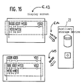
- Figure 15 is a block diagram illustrating registration and reutilization of a "common" ladder diagram in the conventional unit.
- the numeral (24) indicates an input means such as a keyboard, (2a) a control means for controlling internal operation in accordance with input data, (3a) a ladder program writing means, (4a) a ladder diagram writing means for fetching a common ladder diagram from a ladder program, and (7a) an auxiliary storage device read/write means for transferring data to and from the auxiliary storage device (23).
- a PC ladder diagram is written by entering ladder symbols and device numbers of the PC from the keyboard (24) by means of the control program stored in the main storage device (22) and the results are displayed on the display device (25).
- the written program is sequentially converted inside the main storage device (22) into a program executable by the corresponding PC. After this conversion, the program can be stored in the auxiliary storage device (23) and/or output to the printer (26).
- a "common" ladder diagram area can be cut from the ladder program as written using the common ladder diagram writing means (4a) and written to the auxiliary storage device (23) via the auxiliary storage device read/write means (7).
- Figure 16 shows the device and sequence of screens and data displayed during the above conventional operation.
- the area of the common ladder diagram enclosed by the dotted line is written to the auxiliary storage device (23) using the writing means (4a) and the auxiliary storage device read/write means (7a). Later, the common ladder diagram is read from the auxiliary storage device (23) through the auxiliary storage device read/write means (7a) and added to the program currently being written.
- the entered ladder symbol and the specified device are displayed in the ladder diagram create/edit area and the cursor moves to the next block.
- the prior art programming unit configured as described above has a disadvantage in that a programmer cannot write a ladder diagram in terms of logical operation expressions because one device must be specified for one symbol, and, also, many keys must be pressed if a complicated ladder diagram is to be written.
- an object of the present invention to overcome the disadvantages in the prior art by providing a PC programming apparatus which uses a ladder diagram technique and will allow multiple devices to be entered as against one ladder symbol, as connected by a logical operator, and to be automatically converted into instruction codes in accordance with the operator.
- a common ladder diagram editor means replaces the device designations specified in the stored common ladder diagram segment with the actual devices used by the PC in accordance with the data in a device comparison table stored in the auxiliary storage device. After the replacement of the device designations is complete, the common ladder diagram is incorporated into the ladder program being written.
- Figure 1 is a block diagram of the hardware of a conventional PC programming unit.
- FIG. 2 is a block diagram showing data and processing flows in the conventional programming unit.
- Figure 3 is a transition diagram of pressed keys and screens in the conventional unit.
- Figure 4 illustrates a ladder diagram edit screen for performing display conversion processing in the conventional unit and in an embodiment of the present invention.
- Figure 5A is a diagram showing the configuration of a screen image table used in the conventional unit and in the embodiment of the present invention and Figure 5B is a illustration of a stored data format.
- Figure 6 is a block diagram illustrating the flow of data processing in a PC programming unit according to an embodiment of the present invention.
- Figure 7 is a transition diagram of pressed keys and screens for an AND function according to an embodiment of the present invention.
- Figure 8 is an illustration of a transition diagram of pressed keys and screens for an OR function according to an embodiment of the present invention.
- Figure 9 is a function block diagram of a programmable controller programming unit according to an embodiment of the invention.
- Figure 10 is a flowchart illustrating the processing of inserting a common ladder diagram into a ladder program.
- Figures 11 to 14 are diagrams illustrating the process shown in Figure 10.
- Figure 15 is a function block diagram illustrating a conventional way of writing and using the common ladder diagram.
- Figure 16 is a diagram illustrating a flow of data in the conventional unit.
- FIG. 6 is a block diagram illustrating the flow of processing and data in writing a ladder diagram.
- the elements identified by reference numerals 12 to 19, 24 and 25 are identical to those in the conventional unit.
- an operator extraction processor 11 for extracting an operator code from the input data in the keyed-in data buffer 12.
- the microprocessor 21 runs a control program, stored in the main storage device 22, which is designed to permit the programming unit to enter a PC program write mode, having a ladder diagram write mode.
- a cursor is displayed at a position where a ladder diagram symbol is to be entered.
- the keyed-in data is displayed in the keyed-in data display area 72 of CRT 25 and temporarily stored in the keyed-in data buffer 12.
- the devices X0 and X1 extracted by the device part extraction processor 14 are converted into respective internal processing codes. Completion of the above processing initiates the operation of screen image table creation processor 17.
- the screen image table creation processor 17 combines the first "LD" instruction with the first device name "X0" and stores it an address in the screen image table shown in Figure 5A relevant to line and column positions of the ladder display/edit area of Figure 4 indicated by the cursor 73 on the display screen.
- the "AND” instruction is combined with the device name "X1" and stored at a relevant address of the screen image table shown in Figure 5A. Since, in the expression of ladder language, an "AND” is represented by simply stringing together the ladder symbols, the processor 17, upon recognizing the presence of an AND operator, controls the block position controller 18 so as to advance the column position by +1 for display of a second "- ⁇ -" and the associated device X1.
- Figure 8 shows the sequence of operations upon entry of an "OR" instruction, wherein the internal processing is identical to that described previously, with the exception that +1 is added to the line position data in Figure 8 by the table creation processor 17.
- an "OR" is indicated by a parallel ladder symbol (see screen 70C'').
- the OR operator is recognized by the processor 176 for this purpose.
- the line count is returned to its original value after processing the OR operator, so that other symbolic instructions can be indicated on the original line, provided that sufficient column space exists in the given line.
- the data of the screen image table is converted into data displayable on the display device by the screen display data conversion processor 19 and displayed on the display screen as the final result of the processing begun by pressing the return key as shown in figures 7 or 8.
- any key indicating termination of entry e.g., and END key or the like, may be employed instead of the return key in the foregoing embodiment, as the trigger to begin processing the input.
- Figure 9 is a block diagram illustrating the apparatus for registration and utilization of a common ladder diagram portion once it is created on the display device (25).
- the numerals (23), (24), (2a) to (4a) and (7a) indicate the same parts as those of the prior art in Figure 15.
- (5a) indicates a device comparison tabulating means for creating a comparison table between device names used in the common ladder diagram and those actually used by the current PC.
- (6a) is a common ladder diagram editing means for replacing the device numbers used in the common ladder diagram in accordance with data from the device comparison table and inserting the ladder program into the original program.
- Figure 10 is a flowchart of a program stored in the main storage device (22) shown in Figure 1 by the common ladder diagram writing means (4a) shown in Figure 9.
- Figure 11 shows an example of a screen displaying a common ladder diagram that is read from the auxiliary storage device (23) using the common ladder diagram writing means (4a).
- Figure 12 shows an example of a screen illustrating setting of the actual device names using the device comparison tabulating means (5a).
- Figure 13 illustrates overall operation of the present invention.
- the common ladder diagram writing means (4a) writes a ladder diagram in a manner similar to the ladder program writing means (3a).
- the ladder program writing means (3a) uses a device number, corresponding to the actual devices employed by the PC, in the ladder program.
- the common ladder diagram writing means (4a) uses fixed device numbers (designated by "FD" in this embodiment), which differ from the actual device numbers used in writing the ladder program.
- the fixed device numbers in the common ladder diagram must be converted to actual device numbers.
- FIG. 13 An example of a common ladder diagram, along with its dedicated device numbers, is indicated by the area enclosed by the dotted line (51) in Figure 13.
- the common ladder diagram after being written, is provided with a serial number and stored in the auxiliary storage device (23) so that it may be recalled when desired.
- a setting screen as shown in Figure 12 is displayed on the display device (25) so that actual device numbers corresponding to the fixed devices FD used by the PC may be entered through the input means (24).
- the device comparison tabulating means (5a) creates a device comparison table relating the device configuration of the PC for which a program is currently being written to the fixed device names used in the stored ladder segments.
- a comparison table can be created for each type of PC device configuration, and thus the stored ladder segments can be used for any configuration after conversion.
- the comparison tables may themselves be stored in auxiliary storage device (23) via auxiliary storage read/write means (7a).
- the common ladder diagram editing means (6a) is activated by input means (24), which may be in the form of a keyboard, via the control means (2a). A sequence of this operation will be described according to the flowchart in Figure 10.
- a common ladder diagram inserting position is specified at step (S21) to determine where to insert the common ladder diagram in the PC ladder program being written. Then, at step (S22), the serial number of the common ladder diagram, to be retrieved from the auxiliary storage device (23) is specified. At step (S23), the specified common ladder diagram is read from the auxiliary storage device (23) via the auxiliary storage device read/write means (7a) and sent to the main storage device 22.
- the device comparison table corresponding to the PC, for which the ladder program is being written is read from the auxiliary storage device (23) and sent to the main storage device (22) via the auxiliary storage device read/write means (7a).
- Figure 14 indicates how the data is stored in the device comparison table once written into the main storage device (22). In Figure 14, an area is secured for each fixed device to store the device number actually used by the PC.
- Step (S25) determines whether the fixed device numbers have been extracted from the common ladder diagram read in step (S24).
- Step (S27) uses the device comparison table, shown in Figure 12, and fetches the actual device numbers corresponding to the fixed devices.
- step (S28) the fixed device numbers are replaced by the actual device numbers. The process is repeated and step (S25) continues searching for fixed device numbers in the common ladder diagram not yet replaced by the actual devices, repeating the processing at steps (S26) to (S28), until replacement of all fixed device numbers is complete.
- Numeral (52) in Figure 13 indicates a common ladder diagram, indicated by (51), in which the fixed device numbers have been converted to actual device numbers in accordance with the device comparison table indicated by (53).
- step (S29) converts the program into a format usable by the ladder program writing means (3a). Then at step (S29), the converted common ladder diagram is inserted into the ladder program at the inserting position specified at step (S21).
- the programmable controller programming process allows a ladder symbol and devices to be combined by an operator code entered from the keyboard. This also permits each operator code to be automatically converted into a instruction so that a ladder symbol need not be entered every time a device is specified. With the above capabilities, excellent operability is ensured in data entry.
- a further advantage is that the programming process will allow a common ladder diagram to be written without relying on PC I/O assignment since the common ladder diagram may be written by specifying devices other than those used by the PC. Therefore, device numbers need not be manually corrected according to the PC I/O assignment when the common ladder diagram is used to write a PC ladder diagram, and the device comparison table for the PC corresponding to the program must only be created once. By writing a multiple of those common ladder diagrams, PC programming can be achieved efficiently.
Claims (8)
- Verfahren zum Leiterprogrammieren einer programmierbaren Steuerung, die einen Mikroprozessor (21), eine Speichereinrichtung (12), eine Eingabeeinrichtung (24) und eine Anzeigeeinrichtung (25) aufweist, durch Anwendung einer Leiterprogrammierungstechnik, die die folgenden Schritte aufweist:a) Eingeben von Leitersymboldaten und Geräteidentifizierungsdaten an der Eingabeeinrichtung (24), um eine Vielzahl von Geräten (X0, X1) zu bezeichnen;b) Zwischenspeichern der eingegebenen Daten in der Speichereinrichtung (12);c) Entnehmen der gespeicherten Daten;d) Umwandeln der Leitersymboldaten und der Geräteidentifizierungsdaten in Codes und Assemblieren der Codes als einen Programmbefehl; unde) Anzeigen des Programmbefehls in Leiterform auf der Anzeigeeinrichtung (25);gekennzeichnet durchf) in den Schritten a) und b), zusätzliches Eingeben und Speichern von logischen Operatordaten, die eine Kombination der bezeichneten Geräte (X0, X1) definieren;g) in Schritt c), Entnehmen der logischen Operatordaten und der Daten der bezeichneten Geräte (X0, X1), um logisch verknüpft zu werden;h) in Schritt d), Umwandeln der logischen Operatordaten in einen Operatorcode und Assemblieren von Programmbefehlen nach Maßgabe der Leitersymbolcodes und des Operatorcodes, der die bezeichneten Geräte (X0, X1) verknüpft.
- Verfahren nach Anspruch 1, dadurch gekennzeichnet, daß es die folgenden weiteren Schritte aufweist:Zwischenanzeigen der eingegebenen Daten auf der Anzeigeeinrichtung (25); undIdentifizieren des Endes des Dateneingabeschritts, so daß die Daten in einen Programmbefehl umgewandelt werden, der aufgrund des Identifizierungsschritts in Leiterform auf der Anzeigeeinrichtung (25) angezeigt wird.
- Verfahren nach Anspruch 1 oder Anspruch 2, dadurch gekennzeichnet, daß der Operatorcode wirksam ist, um die miteinander verbundenen Geräte in dem Entnahmeschritt zu trennen und die Geräte mit einem entsprechenden Leitersymbol zu verbinden.
- Verfahren nach einem der Ansprüche 1 bis 3, dadurch gekennzeichnet, daß es den weiteren Schritt aufweist: Anzeigen der eingegebenen Daten auf der Anzeigeeinrichtung (25) aufgrund von Adresseninformation, die von einem Cursor (73) geliefert wird.
- Verfahren nach einem der Ansprüche 1 bis 4, dadurch gekennzeichnet, daß es ferner die folgenden Schritte aufweist:Schreiben eines gemeinsamen Leiterdiagramms (51) unter Verwendung von Gerätenummern eines ersten Typs, die in einem Format sind, das mit Gerätenummern eines zweiten Typs, die in einer PC-Gerätekonfiguration verwendet werden, inkompatibel ist;Erzeugen einer Vergleichstabelle (Fig. 14) zwischen den Gerätenummern vom ersten Typ und den Gerätenummern vom zweiten Typ durch eine Gerätevergleichs-Tabelliereinrichtung (51), wobei die Gerätenummern vom zweiten Typ in einem Format sind, das mit denjenigen kompatibel ist, die in einer bestimmten PC-Gerätekonfiguration in Gebrauch sind;Ersetzen (S28) der Gerätenummern vom ersten Typ in dem gemeinsamen Leiterdiagramm (51) durch entsprechende Gerätenummern vom zweiten Typ aus der Vergleichstabelle unter Verwendung einer gemeinsamen Leiterdiagramm-Aufbereitungseinrichtung (6a); undEinfügen (S30) des gemeinsamen Leiterdiagramms (51) in das gerade geschriebene Leiterprogramm, nachdem die Gerätenummern vom ersten Typ in dem gemeinsamen Leiterdiagramm (51) durch die entsprechenden Gerätenummern vom zweiten Typ ersetzt worden sind.
- Programmiervorrichtung für eine programmierbare Steuerung, wobei die Programmiervorrichtung aufweist: einen Mikroprozessor (21), eine Anzeigeeinrichtung (25) mit einem Anzeigefeld (70), eine Zwischenspeichereinrichtung (12), Einrichtungen (24), um in den Zwischenspeicher Leitersymboldaten und Geräteidentifikationsdaten zur Bezeichnung einer Vielzahl von Geräten (X0, X1) einzugeben, Entnahmeeinrichtungen (11, 13, 14) und Umwandlungseinrichtungen (15, 16) zur Entnahme und Codierung der Leitersymbol- und Geräteidentifikationsdaten in Codes, und eine Bildschirmdarstellung-Tabellenerzeugungseinrichtung (17), um an einzeln adressierten Stellen die Leitersymbol- und Geräteidentifikationscodes zur Verwendung bei der Erzeugung einer Anzeige auf der Anzeigeeinrichtung (25) zu speichern, dadurch gekennzeichnet, daßdie Eingabeeinrichtungen (24) ausgebildet sind, um logische Operatordaten in die Zwischenspeichereinrichtung (12) einzugeben, wobei die Operatordaten eine Kombination der bezeichneten Geräte (X0, X1) definieren,die Entnahmeeinrichtungen (11, 13, 14) eine Einrichtung (14) aufweisen, um die Geräteidentifikationsdaten für jedes der bezeichneten Geräte (X0, X1) zu trennen und zu speichern, und ferner eine Operatorentnahmeeinrichtung (11) zur Entnahme der Operatordaten aufweisen;die Umwandlungseinrichtungen (15) ausgebildet sind, um Codes nach Maßgabe der entnommenen logischen Operatordaten zu erzeugen; unddie Bildschirmdarstellung-Tabellenerzeugungseinrichtung (17) ausgebildet ist, um die codierte Information als Programmbefehle zu assemblieren und zu speichern nach Maßgabe der Leitersymbolcodes und der Operatorcodes, um die bezeichneten Geräte (X0, X1) zu kombinieren.
- Vorrichtung nach Anspruch 6, dadurch gekennzeichnet, daß sie ferner eine Blockpositionssteuereinrichtung (18) aufweist, die auf Codes von der Umwandlungseinrichtung (15) und der Bildschirmdarstellung-Tabellenerzeugungseinrichtung (17) anspricht, um eine Adresse zu identifizieren, an der die Information gespeichert werden soll.
- Vorrichtung nach Anspruch 7, dadurch gekennzeichnet, daß die Adresse aufgrund des Operatorcodes um einen vorbestimmten Betrag inkrementiert wird.
Priority Applications (1)
| Application Number | Priority Date | Filing Date | Title |
|---|---|---|---|
| EP94116096A EP0635772B1 (de) | 1990-03-02 | 1991-02-27 | Vorrichtung zur Programmierung einer speicherprogrammierbaren Steuerung und Diagrammtechnik |
Applications Claiming Priority (2)
| Application Number | Priority Date | Filing Date | Title |
|---|---|---|---|
| JP2051106A JP2526692B2 (ja) | 1990-03-02 | 1990-03-02 | プログラマブルコントロ―ラのプログラミング方法 |
| JP51106/90 | 1990-03-02 |
Related Child Applications (1)
| Application Number | Title | Priority Date | Filing Date |
|---|---|---|---|
| EP94116096.2 Division-Into | 1991-02-27 |
Publications (2)
| Publication Number | Publication Date |
|---|---|
| EP0444655A1 EP0444655A1 (de) | 1991-09-04 |
| EP0444655B1 true EP0444655B1 (de) | 1996-06-05 |
Family
ID=12877556
Family Applications (2)
| Application Number | Title | Priority Date | Filing Date |
|---|---|---|---|
| EP94116096A Expired - Lifetime EP0635772B1 (de) | 1990-03-02 | 1991-02-27 | Vorrichtung zur Programmierung einer speicherprogrammierbaren Steuerung und Diagrammtechnik |
| EP91102966A Expired - Lifetime EP0444655B1 (de) | 1990-03-02 | 1991-02-27 | Vorrichtung zur Programmierung einer speicherprogrammierbaren Steuerung und Verfahren zum Gebrauch der Ablaufplantechnik |
Family Applications Before (1)
| Application Number | Title | Priority Date | Filing Date |
|---|---|---|---|
| EP94116096A Expired - Lifetime EP0635772B1 (de) | 1990-03-02 | 1991-02-27 | Vorrichtung zur Programmierung einer speicherprogrammierbaren Steuerung und Diagrammtechnik |
Country Status (4)
| Country | Link |
|---|---|
| US (1) | US5586335A (de) |
| EP (2) | EP0635772B1 (de) |
| JP (1) | JP2526692B2 (de) |
| DE (2) | DE69126042T2 (de) |
Cited By (2)
| Publication number | Priority date | Publication date | Assignee | Title |
|---|---|---|---|---|
| EP0860758A1 (de) * | 1997-02-22 | 1998-08-26 | Robert Bosch Gmbh | Einrichtung zur Programmierung einer SPS |
| US5841657A (en) * | 1991-03-30 | 1998-11-24 | Mazda Motor Corporation | System designing method of a production line |
Families Citing this family (18)
| Publication number | Priority date | Publication date | Assignee | Title |
|---|---|---|---|---|
| US5862401A (en) * | 1994-10-11 | 1999-01-19 | Crown International, Inc. | Programmable central intelligence controller and distributed intelligence network for analog/digital control systems |
| US5623401A (en) * | 1995-08-16 | 1997-04-22 | Allen-Bradley Company, Inc. | Industrial controller with optimized execution of relay ladder logic programs |
| US5764507A (en) * | 1996-01-02 | 1998-06-09 | Chuo; Po-Chou | Programmable controller with personal computerized ladder diagram |
| US6952811B1 (en) * | 1998-07-30 | 2005-10-04 | Mitsubishi Denki Kabushiki Kaisha | Ladder circuit editing system |
| US6167319A (en) * | 1998-10-13 | 2000-12-26 | Scientronix, Inc. | Process for generating program listings for programming a logic control unit |
| JP2002007299A (ja) | 2000-06-21 | 2002-01-11 | Mitsubishi Electric Corp | デバイス制御プログラム開発手段及び実行手段 |
| JP2003256203A (ja) | 2002-03-01 | 2003-09-10 | Mitsubishi Electric Corp | 自動機アプリケーションプログラム開発システム、プログラム開発方法、この方法を実行するプログラム、及びこのプログラムを記憶した記憶媒体 |
| FR2852714B1 (fr) * | 2003-03-17 | 2005-05-06 | Schneider Electric Ind Sas | Procede de programmation d'un automatisme |
| DE10342014B4 (de) * | 2003-09-11 | 2012-08-30 | Siemens Ag | Verfahren zum Ansteuern einer Einheit einer technischen Vorrichtung |
| US20070078540A1 (en) * | 2005-10-05 | 2007-04-05 | Invensys Systems, Inc. | Utility for comparing deployed and archived parameter value sets within a field device editor |
| US8448149B2 (en) * | 2007-02-19 | 2013-05-21 | Schneider Electric Automation Gmbh | Method for the conversion of ladder diagrams |
| JP5138090B2 (ja) * | 2009-02-18 | 2013-02-06 | 三菱電機株式会社 | プログラム解析支援装置 |
| CN101566839B (zh) * | 2009-06-01 | 2011-03-30 | 杭州电子科技大学 | 一种梯形图内嵌组态算法的实现方法 |
| WO2014080531A1 (ja) * | 2012-11-26 | 2014-05-30 | 三菱電機株式会社 | ラダープログラム表示装置およびラダープログラム表示方法 |
| US9626160B2 (en) | 2013-03-29 | 2017-04-18 | Mitsubishi Electric Corporation | Sequence-program-component creation program and sequence-program-component creation device |
| WO2018051441A1 (ja) * | 2016-09-14 | 2018-03-22 | 三菱電機株式会社 | ラダープログラム編集支援装置およびラダープログラムの編集方法 |
| US10154122B1 (en) | 2017-09-05 | 2018-12-11 | Sonos, Inc. | Grouping in a system with multiple media playback protocols |
| CN113518947B (zh) * | 2019-03-05 | 2022-10-21 | 三菱电机株式会社 | 程序创建辅助装置、程序创建辅助方法及储存有程序创建辅助程序的记录介质 |
Family Cites Families (19)
| Publication number | Priority date | Publication date | Assignee | Title |
|---|---|---|---|---|
| US4247909A (en) * | 1979-01-09 | 1981-01-27 | Westinghouse Electric Corp. | Programmable dual stack relay ladder diagram line solver with shift register |
| JPS55135908A (en) * | 1979-04-11 | 1980-10-23 | Hitachi Ltd | Sequence program input device |
| JPS56118106A (en) * | 1980-02-21 | 1981-09-17 | Mitsubishi Electric Corp | Sequence controller |
| JPS56168263A (en) * | 1980-05-30 | 1981-12-24 | Hitachi Ltd | Program making device |
| JPS5750008A (en) * | 1980-09-08 | 1982-03-24 | Hitachi Ltd | Sequence generator |
| JPS57132207A (en) * | 1981-02-10 | 1982-08-16 | Toyoda Mach Works Ltd | Online monitor device of sequence controller |
| JPS57206908A (en) * | 1981-06-15 | 1982-12-18 | Hitachi Ltd | Sequence forming device |
| US5126956A (en) * | 1982-03-11 | 1992-06-30 | Fanuc Ltd | Method and apparatus for displaying segments of a ladder diagram which turn on an operator specified relay |
| JPS58155414A (ja) * | 1982-03-11 | 1983-09-16 | Fanuc Ltd | ラダ−ダイヤグラム表示方式 |
| JPS58155415A (ja) * | 1982-03-11 | 1983-09-16 | Fanuc Ltd | ラダ−ダイヤグラム表示方式 |
| US4870614A (en) * | 1984-08-02 | 1989-09-26 | Quatse Jesse T | Programmable controller ("PC") with co-processing architecture |
| JPS61123909A (ja) * | 1984-11-20 | 1986-06-11 | Fanuc Ltd | セルコントロ−ルシステム |
| JPS6318401A (ja) * | 1986-07-11 | 1988-01-26 | Hitachi Ltd | プログラマブルコントロ−ラ用プログラミング装置 |
| JPS63200203A (ja) * | 1987-02-14 | 1988-08-18 | Matsushita Electric Works Ltd | シ−ケンスプログラム入力装置 |
| JPH01147701A (ja) * | 1987-12-04 | 1989-06-09 | Fuji Electric Co Ltd | プログラム表示装置 |
| US4939437A (en) * | 1988-06-22 | 1990-07-03 | Siemens Energy & Automation, Inc. | Motor controller |
| US4991076A (en) * | 1989-06-30 | 1991-02-05 | Icom Inc. | Method and apparatus for creating custom displays for monitoring ladder logic programs |
| US5058052A (en) * | 1989-10-16 | 1991-10-15 | Ge Fanuc Automation North America, Inc. | Method for checking the syntax of an instruction list program to determine if the program is expressible as a relay ladder diagram by a programmable logic controller |
| US5212631A (en) * | 1990-08-31 | 1993-05-18 | Allen-Bradley Company, Inc. | Programmable controller processor module having multiple program instruction execution sections |
-
1990
- 1990-03-02 JP JP2051106A patent/JP2526692B2/ja not_active Expired - Lifetime
-
1991
- 1991-02-27 EP EP94116096A patent/EP0635772B1/de not_active Expired - Lifetime
- 1991-02-27 DE DE69126042T patent/DE69126042T2/de not_active Expired - Fee Related
- 1991-02-27 DE DE69119930T patent/DE69119930T2/de not_active Expired - Fee Related
- 1991-02-27 EP EP91102966A patent/EP0444655B1/de not_active Expired - Lifetime
-
1994
- 1994-06-06 US US08/254,423 patent/US5586335A/en not_active Expired - Fee Related
Cited By (2)
| Publication number | Priority date | Publication date | Assignee | Title |
|---|---|---|---|---|
| US5841657A (en) * | 1991-03-30 | 1998-11-24 | Mazda Motor Corporation | System designing method of a production line |
| EP0860758A1 (de) * | 1997-02-22 | 1998-08-26 | Robert Bosch Gmbh | Einrichtung zur Programmierung einer SPS |
Also Published As
| Publication number | Publication date |
|---|---|
| JPH03252801A (ja) | 1991-11-12 |
| DE69119930D1 (de) | 1996-07-11 |
| EP0635772A1 (de) | 1995-01-25 |
| JP2526692B2 (ja) | 1996-08-21 |
| EP0444655A1 (de) | 1991-09-04 |
| DE69126042D1 (de) | 1997-06-12 |
| DE69119930T2 (de) | 1996-11-28 |
| US5586335A (en) | 1996-12-17 |
| DE69126042T2 (de) | 1997-11-13 |
| EP0635772B1 (de) | 1997-05-07 |
Similar Documents
| Publication | Publication Date | Title |
|---|---|---|
| EP0444655B1 (de) | Vorrichtung zur Programmierung einer speicherprogrammierbaren Steuerung und Verfahren zum Gebrauch der Ablaufplantechnik | |
| JP2765423B2 (ja) | プログラマブルコントローラ及びその制御方法 | |
| US4455619A (en) | Interactive equipment for computer programming by linkage of labeled block representations of arithmetic/logical subprograms | |
| US4831580A (en) | Program generator | |
| US4736340A (en) | Processor generating control programs for a programmable controller | |
| EP3540536A2 (de) | Entwicklungsunterstützungsvorrichtung, entwicklungsunterstützungsverfahren und entwicklungsunterstützungsprogramm | |
| US5717588A (en) | Programming system | |
| EP0162380A2 (de) | Tabelliersystem | |
| JPH09230915A (ja) | プログラミング装置 | |
| EP0148948A1 (de) | Fixierverfahren für daten in einer numerischen regelvorrichtung | |
| KR100432407B1 (ko) | 사다리형회로 편집장치 | |
| EP0827053A1 (de) | Programmiersystem für bewegungsregler | |
| EP0416509A2 (de) | Programmierbare Steuerung, Verfahren und Vorrichtung zur Programmierung derselbigen | |
| JP2643540B2 (ja) | Nc言語で作成されたプログラムの自然言語化表示方法およびその装置 | |
| JP2982490B2 (ja) | Sfcプログラミング方式 | |
| GB2175112A (en) | Sequence control method and apparatus | |
| EP0372086A1 (de) | Verfahren zum festlegen des ausgabeformates von numerischen steuerdaten | |
| JPH0519817A (ja) | シーケンス・プログラムの編集方式 | |
| EP0315172A2 (de) | Automatische Programmerzeugung mit Datenstruktursichtanzeige | |
| EP0495992A1 (de) | Verfahren zur korrigierung von leiterprogramm | |
| JP4759996B2 (ja) | 手順入力装置、手順入力システム、手順入力方法及び手順入力プログラム | |
| JP2700013B2 (ja) | プログラマブルコントローラのためのユーザプログラム用コンパイラ | |
| JPH077839U (ja) | 数値制御装置 | |
| JP3000987B2 (ja) | 数値制御装置 | |
| JPH08339208A (ja) | プログラマブルコントローラのプログラム作成装置 |
Legal Events
| Date | Code | Title | Description |
|---|---|---|---|
| PUAI | Public reference made under article 153(3) epc to a published international application that has entered the european phase |
Free format text: ORIGINAL CODE: 0009012 |
|
| AK | Designated contracting states |
Kind code of ref document: A1 Designated state(s): DE FR SE |
|
| 17P | Request for examination filed |
Effective date: 19920218 |
|
| 17Q | First examination report despatched |
Effective date: 19940204 |
|
| RBV | Designated contracting states (corrected) |
Designated state(s): DE SE |
|
| GRAA | (expected) grant |
Free format text: ORIGINAL CODE: 0009210 |
|
| AK | Designated contracting states |
Kind code of ref document: B1 Designated state(s): DE SE |
|
| XX | Miscellaneous (additional remarks) |
Free format text: TEILANMELDUNG 94116096.2 EINGEREICHT AM 27/02/91. |
|
| REF | Corresponds to: |
Ref document number: 69119930 Country of ref document: DE Date of ref document: 19960711 |
|
| PLBE | No opposition filed within time limit |
Free format text: ORIGINAL CODE: 0009261 |
|
| STAA | Information on the status of an ep patent application or granted ep patent |
Free format text: STATUS: NO OPPOSITION FILED WITHIN TIME LIMIT |
|
| 26N | No opposition filed | ||
| PGFP | Annual fee paid to national office [announced via postgrant information from national office to epo] |
Ref country code: SE Payment date: 20010206 Year of fee payment: 11 |
|
| PGFP | Annual fee paid to national office [announced via postgrant information from national office to epo] |
Ref country code: DE Payment date: 20010221 Year of fee payment: 11 |
|
| PG25 | Lapsed in a contracting state [announced via postgrant information from national office to epo] |
Ref country code: SE Free format text: LAPSE BECAUSE OF NON-PAYMENT OF DUE FEES Effective date: 20020228 |
|
| PG25 | Lapsed in a contracting state [announced via postgrant information from national office to epo] |
Ref country code: DE Free format text: LAPSE BECAUSE OF NON-PAYMENT OF DUE FEES Effective date: 20020903 |
|
| EUG | Se: european patent has lapsed |
Ref document number: 91102966.8 |