EP0442818A2 - FM-Demodulator - Google Patents
FM-Demodulator Download PDFInfo
- Publication number
- EP0442818A2 EP0442818A2 EP91400386A EP91400386A EP0442818A2 EP 0442818 A2 EP0442818 A2 EP 0442818A2 EP 91400386 A EP91400386 A EP 91400386A EP 91400386 A EP91400386 A EP 91400386A EP 0442818 A2 EP0442818 A2 EP 0442818A2
- Authority
- EP
- European Patent Office
- Prior art keywords
- equalizer
- circuit
- signal
- output
- sideband components
- Prior art date
- Legal status (The legal status is an assumption and is not a legal conclusion. Google has not performed a legal analysis and makes no representation as to the accuracy of the status listed.)
- Granted
Links
Images

Classifications
-
- H—ELECTRICITY
- H04—ELECTRIC COMMUNICATION TECHNIQUE
- H04N—PICTORIAL COMMUNICATION, e.g. TELEVISION
- H04N5/00—Details of television systems
- H04N5/76—Television signal recording
- H04N5/91—Television signal processing therefor
- H04N5/93—Regeneration of the television signal or of selected parts thereof
- H04N5/931—Regeneration of the television signal or of selected parts thereof for restoring the level of the reproduced signal
- H04N5/9315—Regeneration of the television signal or of selected parts thereof for restoring the level of the reproduced signal the level control being frequency dependent
-
- H—ELECTRICITY
- H03—ELECTRONIC CIRCUITRY
- H03D—DEMODULATION OR TRANSFERENCE OF MODULATION FROM ONE CARRIER TO ANOTHER
- H03D3/00—Demodulation of angle-, frequency- or phase- modulated oscillations
- H03D3/02—Demodulation of angle-, frequency- or phase- modulated oscillations by detecting phase difference between two signals obtained from input signal
- H03D3/04—Demodulation of angle-, frequency- or phase- modulated oscillations by detecting phase difference between two signals obtained from input signal by counting or integrating cycles of oscillations
-
- H—ELECTRICITY
- H04—ELECTRIC COMMUNICATION TECHNIQUE
- H04N—PICTORIAL COMMUNICATION, e.g. TELEVISION
- H04N9/00—Details of colour television systems
- H04N9/79—Processing of colour television signals in connection with recording
- H04N9/7908—Suppression of interfering signals at the reproducing side, e.g. noise
- H04N9/7912—Suppression of interfering signals at the reproducing side, e.g. noise the interfering signals being intermodulation signals
Definitions
- the present invention relates generally to an FM demodulating apparatus, and more particularly, to an FM demodulating apparatus of this kind which is suitable for use in demodulation or the like of video signals recorded by, for example, a video tape recorder (hereinafter simply called "VTR") by an FM modulation (frequency modulation).
- VTR video tape recorder
- video signals recorded on a magnetic tape by FM modulation are reproduced from the magnetic tape and FM demodulated, for example, in a VTR (video tape recorder).
- a reproduced video signal fed to an input terminal 1 is supplied to an RF signal equalizer (RF equalizer) 2 wherein characteristics of sideband components of the reproduced video signal are equalized so as to be equivalent to the modulation figure of an FM modulation signal upon recording.
- the output from the RF signal equalizer 2 is supplied to an FM demodulation circuit 3 to be FM demodulated.
- a pulse counter type FM demodulation circuit is used, as the FM demodulation circuit 3.
- the demodulated output from the FM demodulation circuit 3 is delivered to a demodulated video signal output terminal 4.
- Such an FM demodulating apparatus demodulates a signal in a wide range of the modulation figures so that reproduction characteristics of upper sideband components may be easily fluctuated due to conditions of reproducing heads and a magnetic tape and so on of a VTR, which causes drop-out of information called reverse phenomenon and accordingly easy generation of noise on a demodulated signal.
- the FM demodulating apparatus is comprised of a first equalizer for equalizing incoming FM modulated video signals by suppressing sideband components of the incoming video signals, an FM demodulator circuit connected to the first equalizer,wherein the FM demodulator circuit is a pulse counter type FM demodulator, and a second equalizer connected to the FM demodulator circuit for equalizing demodulated video signals from the FM demodulator circuit by recovering suppressed sideband components and for deriving output video signals.
- characteristics of side band components of a reproduced video signal fed to an input terminal 1 are equalized by an RF signal equalizer 2 so as to be equivalent to a modulation figure of an FM modulation signal upon recording, and then the equalized output video signal from the RF signal equalizer 2 is supplied to an FM demodulating apparatus 10.
- the FM demodulating apparatus 10 comprises a sine equalizer 20, a pulse counter type FM demodulation circuit 30 and a cosine equalizer 40.
- the output video signal from the RF signal equalizer 2 is supplied to the sine equalizer 20 which functions as a bandpass filter for suppressing sideband components for the carrier of an FM modulated signal.
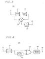
- the sine equalizer 20 is constructed as shown in Fig. 3, for example.
- a signal fed to a terminal 21 is supplied to a series circuit composed of two delay circuits 22, 23 for providing a delay amount ⁇ ( ⁇ is the unit delay amount). Then, the signal supplied to the terminal 21 and the output signal from the delay circuit 23 are supplied to a subtractor 24 to subtract the signal delayed by the delay circuits 22, 23 from the input signal. The subtraction output from the subtractor 24 is delivered to an output terminal 26 through a 1/2 attenuator 25.
- the peak (1/4 ⁇ ) of the sine wave is substantially equal to the central frequency of the carrier so that the sine equalizer 20 functions as a bandpass filter for suppressing sideband components for the carrier.
- the output from the sine equalizer 20 is then supplied to a pulse count type FM demodulation circuit 30.
- Fig. 4 shows the configuration of a practical example of the pulse count type FM demodulation circuit 30.
- An FM modulated signal supplied from the sine equalizer 20 to an input terminal 31 is band limited by a limiter 32 and thereafter supplied directly to an Exclusive-OR gate 33 as well as to the Exclusive-OR gate 33 through a delay circuit 34.
- An exclusive logical OR outputted from the Exclusive-OR gate 33 is delivered to an output terminal 36 through a low pass filter 35.
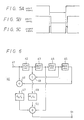
- the Exclusive-OR circuit 33 derives an exclusive logical OR of the input signal and the signal of the input signal delayed by the delay circuit 34 shown in Fig. 5B, and a pulse signal shown in Fig. 5C is outputted from the Exclusive-OR circuit 33.
- the number of the output pulses varies in accordance with the frequency of input signal. Demodulated signals are therefore derived by supplying the output pulses of the Exclusive-OR circuit 33 to the low pass filter 35 and averaging the same thereby.
- the output signal from the FM demodulation circuit 30 thus constructed is supplied to the cosine equalizer 40 which is provided for recovering the sideband components suppressed by the sine equalizer 20 and constructed as shown in Fig. 6.
- a signal fed to a terminal 41 is supplied to a series circuit composed of four delay circuits 42, 43, 44 and 45 respectively having a delay amount ⁇ . Then, the signal fed to the terminal 41 and the output signal from the delay circuit 45 are supplied to an adder 46 to be added.
- the addition output from the adder 46 is next supplied to an adder 50 through a coefficient multiplier 47 for multiplying a supplied signal by a coefficient (a2/2).
- the output signal from the delay circuit 42 and the output signal from the delay circuit 44 are supplied to an adder 48 to be added.
- the addition output from the adder 48 is supplied to the adder 50 through a coefficient multiplier 49 for multiplying a supplied signal by a coefficient (a1/2). Further, the output signal from the delay circuit 43 is also supplied to the adder 50 which in turn delivers the addition output thereof to an output terminal 51.
- the sideband components suppressed by the sine equalizer 20 is recovered by the cosine equalizer 40.
- the output from the cosine equalizer 40 is then delivered to an output terminal 4 as a demodulated output by the FM demodulating apparatus 10.
- an inputted FM modulated signal S(t) fed to the terminal 1 is expressed by the following equation (1):
- the cosine equalizer 40 is constructed, as shown in Fig. 6, so as to have the characteristics of 1/cos ⁇ , thereby making it possible to derive a demodulated signal with flat frequency characteristics at the demodulated signal output terminal 4 of the FM demodulating apparatus 10 through the cosine equalizer 40.
- the both sideband components have been suppressed by the sine equalizer 20, so that the modulation figure is equivalently lowered and fluctuations in amplitude are reduced, whereby a margin for distortion of the modulated signal is increased, which results in performing a favorable demodulation without reverse phenomenon even if a contact condition between the head and tape is changed and thereby distortion occurs in a reproduced signal, for example, upon reproducing by a VTR.
- the demodulated signal is recovered to have the original frequency characteristics by the cosine equalizer 40 so that the frequency characteristics of the demodulated signal will never be disturbed.
- the pulse count type demodulator employed as the FM demodulation circuit 30 in the present embodiment inconveniently generates undesirable components called moire at a frequency double the carrier frequency, however, the construction of the present embodiment can equivalently lower the modulation figure and therefore prevent such moires from occurring.
- the above described embodiment employs a sine equalizer as a suppressing means for suppressing sideband components of FM modulated signals prior to FM demodulation.
- the sideband components may be suppressed by an ordinary bandpass filter.
- any filter circuit may be used as long as it has characteristics which permit recovering the suppressed sideband components to the original form.
- the FM demodulating apparatus of the present invention since sideband components of FM modulated video signals are suppressed before demodulation performed by an FM demodulation circuit, the equivalent modulation figure is lowered and a margin for distortion of modulated signals is increased, thereby making it possible to achieve favorable demodulation.
- the suppressed sideband components are recovered to have the original frequency characteristics after demodulation, which results in avoiding disturbance of the frequency characteristics of the demodulated signals.
Landscapes
- Engineering & Computer Science (AREA)
- Multimedia (AREA)
- Signal Processing (AREA)
- Power Engineering (AREA)
- Television Signal Processing For Recording (AREA)
Applications Claiming Priority (2)
| Application Number | Priority Date | Filing Date | Title |
|---|---|---|---|
| JP34729/90 | 1990-02-15 | ||
| JP2034729A JPH03237656A (ja) | 1990-02-15 | 1990-02-15 | Fm復調装置 |
Publications (3)
| Publication Number | Publication Date |
|---|---|
| EP0442818A2 true EP0442818A2 (de) | 1991-08-21 |
| EP0442818A3 EP0442818A3 (en) | 1992-01-02 |
| EP0442818B1 EP0442818B1 (de) | 1995-06-21 |
Family
ID=12422408
Family Applications (1)
| Application Number | Title | Priority Date | Filing Date |
|---|---|---|---|
| EP91400386A Expired - Lifetime EP0442818B1 (de) | 1990-02-15 | 1991-02-14 | FM-Demodulator |
Country Status (4)
| Country | Link |
|---|---|
| US (1) | US5200835A (de) |
| EP (1) | EP0442818B1 (de) |
| JP (1) | JPH03237656A (de) |
| DE (1) | DE69110491T2 (de) |
Cited By (1)
| Publication number | Priority date | Publication date | Assignee | Title |
|---|---|---|---|---|
| EP0514154A3 (en) * | 1991-05-15 | 1992-12-16 | Victor Company Of Japan, Ltd. | Apparatus for demodulating an fm image signal |
Families Citing this family (5)
| Publication number | Priority date | Publication date | Assignee | Title |
|---|---|---|---|---|
| US5663844A (en) * | 1990-11-19 | 1997-09-02 | Canon Kabushiki Kaisha | Signal reproducing apparatus having waveform equalizing function |
| US6081155A (en) * | 1998-12-04 | 2000-06-27 | Texas Instruments Incorporated | Digital quadrature discriminator for demodulation of frequency-modulated information |
| KR100657243B1 (ko) * | 1999-10-25 | 2006-12-14 | 삼성전자주식회사 | 비디오 테이프 레코더의 fm 기록 장치 |
| US6440860B1 (en) * | 2000-01-18 | 2002-08-27 | Micron Technology, Inc. | Semiconductor processing methods of transferring patterns from patterned photoresists to materials, and structures comprising silicon nitride |
| US7027505B2 (en) * | 2001-05-04 | 2006-04-11 | Al-Eidan Abdullah A | System and method for bandwidth compression of frequency and phase modulated signals and suppression of the upper and lower sidebands from the transmission medium |
Family Cites Families (12)
| Publication number | Priority date | Publication date | Assignee | Title |
|---|---|---|---|---|
| JPS53117329A (en) * | 1977-03-24 | 1978-10-13 | Hitachi Ltd | Processing circuit for color signal |
| GB2036509B (en) * | 1978-10-27 | 1983-01-26 | Kokusai Denshin Denwa Co Ltd | Automatic phase and amplitude equalisation of fm signals |
| US4591930A (en) * | 1983-09-23 | 1986-05-27 | Eastman Kodak Company | Signal processing for high resolution electronic still camera |
| US4843334A (en) * | 1986-12-09 | 1989-06-27 | Canon Kabushiki Kaisha | Frequency demodulator operable with low frequency modulation carriers |
| JPS63184486A (ja) * | 1987-01-26 | 1988-07-29 | Nec Home Electronics Ltd | 巡回型雑音低減装置 |
| JP2554678B2 (ja) * | 1987-11-20 | 1996-11-13 | 株式会社東芝 | Fm復調器 |
| US4906942A (en) * | 1987-12-17 | 1990-03-06 | Mitsubishi Denki Kabushiki Kaisha | Frequency demodulator with reversal phenomenon compensation |
| US5067026A (en) * | 1988-05-06 | 1991-11-19 | Sony Corporation | Apparatus for recording and reproducing a video signal |
| JPH0244877A (ja) * | 1989-03-14 | 1990-02-14 | Minolta Camera Co Ltd | 音声記録機能を有したカメラ |
| JPH0279256A (ja) * | 1988-09-14 | 1990-03-19 | Kokusai Denshin Denwa Co Ltd <Kdd> | 光記録媒体を用いたテレビジョン信号の記録再生方式 |
| JPH083939B2 (ja) * | 1988-09-19 | 1996-01-17 | 松下電器産業株式会社 | Fm復調回路 |
| ATE110507T1 (de) * | 1988-09-29 | 1994-09-15 | Siemens Ag | Schaltungsanordnung zum entzerren von in analoger form empfangener digitalsignale. |
-
1990
- 1990-02-15 JP JP2034729A patent/JPH03237656A/ja active Pending
-
1991
- 1991-02-11 US US07/653,614 patent/US5200835A/en not_active Expired - Fee Related
- 1991-02-14 EP EP91400386A patent/EP0442818B1/de not_active Expired - Lifetime
- 1991-02-14 DE DE69110491T patent/DE69110491T2/de not_active Expired - Fee Related
Cited By (2)
| Publication number | Priority date | Publication date | Assignee | Title |
|---|---|---|---|---|
| EP0514154A3 (en) * | 1991-05-15 | 1992-12-16 | Victor Company Of Japan, Ltd. | Apparatus for demodulating an fm image signal |
| US5293245A (en) * | 1991-05-15 | 1994-03-08 | Victor Company Of Japan, Ltd. | Video demodulation apparatus with moire component cancellation |
Also Published As
| Publication number | Publication date |
|---|---|
| EP0442818A3 (en) | 1992-01-02 |
| EP0442818B1 (de) | 1995-06-21 |
| DE69110491T2 (de) | 1995-11-09 |
| US5200835A (en) | 1993-04-06 |
| JPH03237656A (ja) | 1991-10-23 |
| DE69110491D1 (de) | 1995-07-27 |
Similar Documents
| Publication | Publication Date | Title |
|---|---|---|
| EP0442818A2 (de) | FM-Demodulator | |
| GB2218876A (en) | Inversion phenomenon preventing circuit | |
| US4629994A (en) | FM demodulator | |
| JPH05276487A (ja) | デジタル復調装置 | |
| JPH02156793A (ja) | Fm復調回路 | |
| KR950011008B1 (ko) | 영상 신호 복조 장치 | |
| JPS6130396Y2 (de) | ||
| JPS5946048B2 (ja) | 磁気記録再生装置 | |
| JPS59101009A (ja) | 磁気記録再生装置 | |
| Itoga et al. | Two channel FM recording for high-definition baseband signals | |
| EP0300801B1 (de) | Frequenzdemodulationsgerät | |
| JPS6252993B2 (de) | ||
| JP3122261B2 (ja) | Fm復調装置 | |
| JPH027203B2 (de) | ||
| JPS63133358A (ja) | 信号処理回路 | |
| JPH0821198B2 (ja) | 磁気記録再生装置 | |
| JP3330264B2 (ja) | Secam信号再生処理装置 | |
| JPH0432857Y2 (de) | ||
| JPH01192062A (ja) | 磁気録画再生装置 | |
| JPH08111849A (ja) | 磁気記録再生装置 | |
| JPH04372772A (ja) | 情報再生装置 | |
| JPH04183081A (ja) | 画像再生装置 | |
| JPH03238669A (ja) | Fm復調装置 | |
| JPS58159087A (ja) | 映像信号記録再生方式 | |
| JPS63144674A (ja) | 画像情報記録装置 |
Legal Events
| Date | Code | Title | Description |
|---|---|---|---|
| PUAI | Public reference made under article 153(3) epc to a published international application that has entered the european phase |
Free format text: ORIGINAL CODE: 0009012 |
|
| AK | Designated contracting states |
Kind code of ref document: A2 Designated state(s): DE FR GB |
|
| PUAL | Search report despatched |
Free format text: ORIGINAL CODE: 0009013 |
|
| AK | Designated contracting states |
Kind code of ref document: A3 Designated state(s): DE FR GB |
|
| 17P | Request for examination filed |
Effective date: 19920626 |
|
| 17Q | First examination report despatched |
Effective date: 19940725 |
|
| GRAA | (expected) grant |
Free format text: ORIGINAL CODE: 0009210 |
|
| AK | Designated contracting states |
Kind code of ref document: B1 Designated state(s): DE FR GB |
|
| REF | Corresponds to: |
Ref document number: 69110491 Country of ref document: DE Date of ref document: 19950727 |
|
| ET | Fr: translation filed | ||
| PLBE | No opposition filed within time limit |
Free format text: ORIGINAL CODE: 0009261 |
|
| STAA | Information on the status of an ep patent application or granted ep patent |
Free format text: STATUS: NO OPPOSITION FILED WITHIN TIME LIMIT |
|
| 26N | No opposition filed | ||
| PGFP | Annual fee paid to national office [announced via postgrant information from national office to epo] |
Ref country code: DE Payment date: 20010205 Year of fee payment: 11 |
|
| REG | Reference to a national code |
Ref country code: GB Ref legal event code: IF02 |
|
| PGFP | Annual fee paid to national office [announced via postgrant information from national office to epo] |
Ref country code: FR Payment date: 20020212 Year of fee payment: 12 |
|
| PGFP | Annual fee paid to national office [announced via postgrant information from national office to epo] |
Ref country code: GB Payment date: 20020213 Year of fee payment: 12 |
|
| PG25 | Lapsed in a contracting state [announced via postgrant information from national office to epo] |
Ref country code: DE Free format text: LAPSE BECAUSE OF NON-PAYMENT OF DUE FEES Effective date: 20020903 |
|
| PG25 | Lapsed in a contracting state [announced via postgrant information from national office to epo] |
Ref country code: GB Free format text: LAPSE BECAUSE OF NON-PAYMENT OF DUE FEES Effective date: 20030214 |
|
| GBPC | Gb: european patent ceased through non-payment of renewal fee | ||
| PG25 | Lapsed in a contracting state [announced via postgrant information from national office to epo] |
Ref country code: FR Free format text: LAPSE BECAUSE OF NON-PAYMENT OF DUE FEES Effective date: 20031031 |
|
| REG | Reference to a national code |
Ref country code: FR Ref legal event code: ST |