EP0441810B1 - Procede pour placer des modules sur un support - Google Patents
Procede pour placer des modules sur un support Download PDFInfo
- Publication number
- EP0441810B1 EP0441810B1 EP89911775A EP89911775A EP0441810B1 EP 0441810 B1 EP0441810 B1 EP 0441810B1 EP 89911775 A EP89911775 A EP 89911775A EP 89911775 A EP89911775 A EP 89911775A EP 0441810 B1 EP0441810 B1 EP 0441810B1
- Authority
- EP
- European Patent Office
- Prior art keywords
- modules
- subregions
- plt
- module
- placement
- Prior art date
- Legal status (The legal status is an assumption and is not a legal conclusion. Google has not performed a legal analysis and makes no representation as to the accuracy of the status listed.)
- Expired - Lifetime
Links
Images

Classifications
-
- G—PHYSICS
- G06—COMPUTING; CALCULATING OR COUNTING
- G06F—ELECTRIC DIGITAL DATA PROCESSING
- G06F30/00—Computer-aided design [CAD]
- G06F30/30—Circuit design
- G06F30/39—Circuit design at the physical level
- G06F30/392—Floor-planning or layout, e.g. partitioning or placement
Abstract
Claims (12)
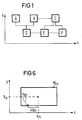
- Procédé pour mettre en place des modules (M) sur un support (T1) à l'aide d'un ordinateur et moyennant l'utilisation d'une liste de modules contenant les dimensions, et d'une liste de réseaux contenant les liaisons, par la mise en oeuvre des étapes opératoires suivantes :a) on dispose selon une mise en place globale, tous les modules mobiles (Mb) dans la zone de mise en place (PL) du support (TR) de telle sorte que le centre de gravité global des modules est situé au niveau du barycentre (Xr, Yr) de la surface de la zone de mise en place, et on dispose tous les modules fixés (Mf) sur les bords de la zone de mise en place;b) lors d'une étape de séparationb1) on subdivise la zone de mise en place (PL) en zones partielles (PLT),b2) ensuite, sur la base de la position des modules fixée lors de l'étape a), on répartit ces modules en des quantités partielles (Mr) de modules et on associe ces quantités partielles aux zones partielles (PLT),b3) ensuite, on fixe de façon définitive la taille des zones partielles dans le rapport des quantités partielles (Mr) des modules, associées aux zones partielles;c) on dispose simultanément les modules (Mb), au moyen d'une mise en place globale, pour toutes les zones partielles (PLT), sous l'influence réciproque, avec chevauchement de zones partielles, au moyen des liaisons contenues dans la liste de réseaux de telle sorte que les centres de gravité globaux des quantités partielles Mr de modules sont situés respectivement au niveau des barycentres (Xr, Yr) des surfaces des zones partielles associées (PLT);d) lors d'une autre étape de séparationd1) on divise les zones partielles en d'autres zones partielles,d2) ensuite, et sur la base de la position des modules (Mb) fixée lors de l'étape c), on associe ces modules aux autres zones partielles (PLT),d3) on fixe ensuite de façon définitive la taille des autres zones partielles dans le rapport des modules associés aux autres zones partielles;e) on répète les étapes c) et d) jusqu'à ce qu'un nombre, pouvant être prédéterminé, de k modules soit associé à chaque zone partielle.
- Procédé suivant la revendication 1, caractérisé par le fait que les points prédéterminés de la zone de mise en place et des zones partielles sont respectivement les coordonnées (Xr, Yr) de leurs centres.
- Procédé suivant la revendication 2, caractérisé par le fait que pour la mise en place globale, les coordonnées (x, y) des modules sont fixées simultanément de telle sorte que l'on a


des symboles dans les formules ayant les significations suivantes :m numéro de modulen numéro de réseauM = (...,m,...) quantité des numéros de modulesN = (...,n,...) quantité des numéros de réseauxMb C M quantité des modules mobilesMf C M quantité des modules fixésb nombre des modules mobilesf nombre des modules fixésx = (...xn...xm...) vecteur des coordonnées x de tous les réseaux et de tous les modulesy = (...xn...xm...) vecteur des coordonnées y de tous les réseaux et de tous les modulesunm coordonnée x de la borne du réseau n au niveau du module mvnm coordonnée y de la borne du réseau m au niveau du module m
dans le cas où il n'y a aucun raccordementwn facteur pondéral du réseau nFm besoin en surface du module mr numéro de la zone de mise en place PL ou de la zone partielle PLTmr C Mb quantité des modules, à laquelle est appliquée la condition secondaire rXr, Yr coordonnées du centre de la zone de mise en place PL, PLTR nombre des zones partielles PLT. - Procédé suivant la revendication 3, caractérisé par le fait que les modules fixés (Mf) sont déplaçables dans la direction x et dans la direction y au niveau des bords de la zone de mise en place (PL).
- Procédé suivant la revendication 4, caractérisé par le fait que l'affectation des modules (M) aux zones partielles (PLT) s'effectue au moyen du tri des modules en fonction de leurs coordonnées (x, y).
- Procédé suivant la revendication 5, caractérisé par le fait que la division de la zone de mise en place et des zones partielles est réalisée par des lignes de coupe horizontales et verticales (SL), et que des quantités partielles de modules (Mr) sont affectées aux zones partielles (PLT) déterminées par les coupes.
- Procédé suivant la revendication 6, caractérisé par le fait que lors de la division, chaque zone est respectivement divisée par deux.
- Procédé suivant la revendication 7, caractérisé par le fait que des modules (M), dont les liaisons associées croisent la ligne de coupe (SL), sont associés aux zones partielles (PLT) moyennant l'application supplémentaire du principe Min-Cut.
- Procédé suivant l'une des revendications 1 à 8, caractérisé par le fait qu'on arrête la mise en place globale et la division lorsqu'un module (M) (k-1) est disposé dans chaque zone partielle.
- Procédé suivant l'une des revendications 1 à 8, caractérisé par le fait que l'utilisation optimale de la surface est obtenue par détermination de toutes les fragmentations possibles des zones partielles (PLT) avec jusqu'à k modules (M) moyennant l'utilisation du résultat de la mise en place globale.
- Procédé suivant la revendication 10, caractérisé par le fait que la disposition des modules (M) dans les zones partielles (PLT) est optimisée par le fait que pour chaque zone partielle on détermine toutes les divisions possibles et qu'on associe les modules aux surfaces partielles obtenues, que pour chaque division et chaque association de modules, on peut calculer les dimensions de la zone rectangulaire la plus petite, dans laquelle les modules peuvent être placés sans chevauchement, et on rassemble les différentes dimensions possibles d'une surface partielle dans une fonction de forme, et qu'on effectue ceci pour toutes les zones partielles (PLT) et qu'on calcule les dimensions de tous les ensembles obtenus de modules, par addition des fonctions de forme de toutes les zones partielles.
- Procédé suivant la revendication 11, caractérisé par le fait qu'on optimise les positions pivotées des modules.
Priority Applications (1)
| Application Number | Priority Date | Filing Date | Title |
|---|---|---|---|
| AT89911775T ATE103403T1 (de) | 1988-11-02 | 1989-10-26 | Verfahren zur plazierung von modulen auf einem traeger. |
Applications Claiming Priority (2)
| Application Number | Priority Date | Filing Date | Title |
|---|---|---|---|
| EP88118251 | 1988-11-02 | ||
| EP88118251 | 1988-11-02 |
Publications (2)
| Publication Number | Publication Date |
|---|---|
| EP0441810A1 EP0441810A1 (fr) | 1991-08-21 |
| EP0441810B1 true EP0441810B1 (fr) | 1994-03-23 |
Family
ID=8199514
Family Applications (1)
| Application Number | Title | Priority Date | Filing Date |
|---|---|---|---|
| EP89911775A Expired - Lifetime EP0441810B1 (fr) | 1988-11-02 | 1989-10-26 | Procede pour placer des modules sur un support |
Country Status (5)
| Country | Link |
|---|---|
| US (1) | US5267176A (fr) |
| EP (1) | EP0441810B1 (fr) |
| JP (1) | JPH04501475A (fr) |
| DE (1) | DE58907307D1 (fr) |
| WO (1) | WO1990005344A1 (fr) |
Families Citing this family (76)
| Publication number | Priority date | Publication date | Assignee | Title |
|---|---|---|---|---|
| US5598344A (en) * | 1990-04-06 | 1997-01-28 | Lsi Logic Corporation | Method and system for creating, validating, and scaling structural description of electronic device |
| JP3220250B2 (ja) * | 1992-01-09 | 2001-10-22 | 株式会社東芝 | セル自動配置方法 |
| US5566078A (en) * | 1993-05-26 | 1996-10-15 | Lsi Logic Corporation | Integrated circuit cell placement using optimization-driven clustering |
| US5598343A (en) * | 1993-10-01 | 1997-01-28 | Texas Instruments Incorporated | Method of segmenting an FPGA channel architecture for maximum routability and performance |
| JP2922404B2 (ja) * | 1993-11-15 | 1999-07-26 | 富士通株式会社 | 集積回路の配置決定方法 |
| US5818726A (en) * | 1994-04-18 | 1998-10-06 | Cadence Design Systems, Inc. | System and method for determining acceptable logic cell locations and generating a legal location structure |
| US6493658B1 (en) | 1994-04-19 | 2002-12-10 | Lsi Logic Corporation | Optimization processing for integrated circuit physical design automation system using optimally switched fitness improvement algorithms |
| US5815403A (en) * | 1994-04-19 | 1998-09-29 | Lsi Logic Corporation | Fail-safe distributive processing method for producing a highest fitness cell placement for an integrated circuit chip |
| US5875117A (en) * | 1994-04-19 | 1999-02-23 | Lsi Logic Corporation | Simultaneous placement and routing (SPAR) method for integrated circuit physical design automation system |
| US6155725A (en) * | 1994-04-19 | 2000-12-05 | Lsi Logic Corporation | Cell placement representation and transposition for integrated circuit physical design automation system |
| US5963975A (en) * | 1994-04-19 | 1999-10-05 | Lsi Logic Corporation | Single chip integrated circuit distributed shared memory (DSM) and communications nodes |
| US5495419A (en) * | 1994-04-19 | 1996-02-27 | Lsi Logic Corporation | Integrated circuit physical design automation system utilizing optimization process decomposition and parallel processing |
| US5914887A (en) * | 1994-04-19 | 1999-06-22 | Lsi Logic Corporation | Congestion based cost factor computing apparatus for integrated circuit physical design automation system |
| US5557533A (en) * | 1994-04-19 | 1996-09-17 | Lsi Logic Corporation | Cell placement alteration apparatus for integrated circuit chip physical design automation system |
| US5535134A (en) * | 1994-06-03 | 1996-07-09 | International Business Machines Corporation | Object placement aid |
| US5638293A (en) * | 1994-09-13 | 1997-06-10 | Lsi Logic Corporation | Optimal pad location method for microelectronic circuit cell placement |
| US5696693A (en) * | 1995-03-31 | 1997-12-09 | Unisys Corporation | Method for placing logic functions and cells in a logic design using floor planning by analogy |
| JP3504394B2 (ja) * | 1995-09-08 | 2004-03-08 | 松下電器産業株式会社 | 部品配列のデータ作成方法 |
| US5818722A (en) * | 1995-11-03 | 1998-10-06 | Yoji Kajitani | Method of placing and extracting modules |
| EP0791887B1 (fr) * | 1996-02-21 | 2001-05-23 | Matsushita Electric Industrial Co., Ltd. | Procédé et dispositif pour l'entrée des topographies des circuits intégrés du type "flip-chip" |
| US5818729A (en) * | 1996-05-23 | 1998-10-06 | Synopsys, Inc. | Method and system for placing cells using quadratic placement and a spanning tree model |
| US5798936A (en) * | 1996-06-21 | 1998-08-25 | Avant| Corporation | Congestion-driven placement method and computer-implemented integrated-circuit design tool |
| US5835381A (en) * | 1996-06-28 | 1998-11-10 | Lsi Logic Corporation | Advanced modular cell placement system with minimizing maximal cut driven affinity system |
| US5867398A (en) * | 1996-06-28 | 1999-02-02 | Lsi Logic Corporation | Advanced modular cell placement system with density driven capacity penalty system |
| US5872718A (en) * | 1996-06-28 | 1999-02-16 | Lsi Logic Corporation | Advanced modular cell placement system |
| US6030110A (en) * | 1996-06-28 | 2000-02-29 | Lsi Logic Corporation | Advanced modular cell placement system with median control and increase in resolution |
| US5870312A (en) * | 1996-06-28 | 1999-02-09 | Lsi Logic Corporation | Advanced modular cell placement system with dispersion-driven levelizing system |
| US5892688A (en) * | 1996-06-28 | 1999-04-06 | Lsi Logic Corporation | Advanced modular cell placement system with iterative one dimensional preplacement optimization |
| US5808899A (en) * | 1996-06-28 | 1998-09-15 | Lsi Logic Corporation | Advanced modular cell placement system with cell placement crystallization |
| US5963455A (en) * | 1996-06-28 | 1999-10-05 | Lsi Logic Corporation | Advanced modular cell placement system with functional sieve optimization technique |
| US5812740A (en) * | 1996-06-28 | 1998-09-22 | Lsi Logic Corporation | Advanced modular cell placement system with neighborhood system driven optimization |
| US5870311A (en) * | 1996-06-28 | 1999-02-09 | Lsi Logic Corporation | Advanced modular cell placement system with fast procedure for finding a levelizing cut point |
| US5844811A (en) * | 1996-06-28 | 1998-12-01 | Lsi Logic Corporation | Advanced modular cell placement system with universal affinity driven discrete placement optimization |
| US5914888A (en) * | 1996-06-28 | 1999-06-22 | Lsi Logic Corporation | Advanced modular cell placement system with coarse overflow remover |
| US6085032A (en) * | 1996-06-28 | 2000-07-04 | Lsi Logic Corporation | Advanced modular cell placement system with sinusoidal optimization |
| US6067409A (en) * | 1996-06-28 | 2000-05-23 | Lsi Logic Corporation | Advanced modular cell placement system |
| US5831863A (en) * | 1996-06-28 | 1998-11-03 | Lsi Logic Corporation | Advanced modular cell placement system with wire length driven affinity system |
| US6026223A (en) * | 1996-06-28 | 2000-02-15 | Scepanovic; Ranko | Advanced modular cell placement system with overlap remover with minimal noise |
| US5980093A (en) * | 1996-12-04 | 1999-11-09 | Lsi Logic Corporation | Integrated circuit layout routing using multiprocessing |
| US6754879B1 (en) | 1997-01-27 | 2004-06-22 | Unisys Corporation | Method and apparatus for providing modularity to a behavioral description of a circuit design |
| US6718520B1 (en) | 1997-01-27 | 2004-04-06 | Unisys Corporation | Method and apparatus for selectively providing hierarchy to a circuit design |
| US6378114B1 (en) * | 1997-07-01 | 2002-04-23 | Synopsys, Inc. | Method for the physical placement of an integrated circuit adaptive to netlist changes |
| US6385760B2 (en) * | 1998-06-12 | 2002-05-07 | Monterey Design Systems, Inc. | System and method for concurrent placement of gates and associated wiring |
| US6378119B1 (en) * | 1999-05-24 | 2002-04-23 | Dell Usa, L.P. | Method and system for adaptive component placement |
| US6415426B1 (en) | 2000-06-02 | 2002-07-02 | Incentia Design Systems, Inc. | Dynamic weighting and/or target zone analysis in timing driven placement of cells of an integrated circuit design |
| US7055120B2 (en) | 2000-12-06 | 2006-05-30 | Cadence Design Systems, Inc. | Method and apparatus for placing circuit modules |
| US6957410B2 (en) | 2000-12-07 | 2005-10-18 | Cadence Design Systems, Inc. | Method and apparatus for adaptively selecting the wiring model for a design region |
| US7024650B2 (en) * | 2000-12-06 | 2006-04-04 | Cadence Design Systems, Inc. | Method and apparatus for considering diagonal wiring in placement |
| US6826737B2 (en) * | 2000-12-06 | 2004-11-30 | Cadence Design Systems, Inc. | Recursive partitioning placement method and apparatus |
| US6516455B1 (en) * | 2000-12-06 | 2003-02-04 | Cadence Design Systems, Inc. | Partitioning placement method using diagonal cutlines |
| US7080336B2 (en) | 2000-12-06 | 2006-07-18 | Cadence Design Systems, Inc. | Method and apparatus for computing placement costs |
| JP2004529402A (ja) * | 2000-12-06 | 2004-09-24 | シンプレックス ソリューションズ、インコーポレイテッド | 配置の際に対角線配線を考慮に入れるための方法および装置 |
| US7003754B2 (en) * | 2000-12-07 | 2006-02-21 | Cadence Design Systems, Inc. | Routing method and apparatus that use of diagonal routes |
| US7073150B2 (en) | 2000-12-07 | 2006-07-04 | Cadence Design Systems, Inc. | Hierarchical routing method and apparatus that use diagonal routes |
| US6915501B2 (en) | 2001-01-19 | 2005-07-05 | Cadence Design Systems, Inc. | LP method and apparatus for identifying routes |
| US6738960B2 (en) * | 2001-01-19 | 2004-05-18 | Cadence Design Systems, Inc. | Method and apparatus for producing sub-optimal routes for a net by generating fake configurations |
| US6507937B1 (en) * | 2001-06-19 | 2003-01-14 | Lsi Logic Corporation | Method of global placement of control cells and hardmac pins in a datapath macro for an integrated circuit design |
| US6795958B2 (en) | 2001-08-23 | 2004-09-21 | Cadence Design Systems, Inc. | Method and apparatus for generating routes for groups of related node configurations |
| US7143382B2 (en) | 2001-08-23 | 2006-11-28 | Cadence Design Systems, Inc. | Method and apparatus for storing routes |
| US6931616B2 (en) * | 2001-08-23 | 2005-08-16 | Cadence Design Systems, Inc. | Routing method and apparatus |
| US6745379B2 (en) | 2001-08-23 | 2004-06-01 | Cadence Design Systems, Inc. | Method and apparatus for identifying propagation for routes with diagonal edges |
| US7058913B1 (en) | 2001-09-06 | 2006-06-06 | Cadence Design Systems, Inc. | Analytical placement method and apparatus |
| US7225116B2 (en) * | 2002-08-20 | 2007-05-29 | Cadence Design Systems, Inc. | Method for eliminating routing congestion in an IC layout |
| US7080342B2 (en) * | 2002-11-18 | 2006-07-18 | Cadence Design Systems, Inc | Method and apparatus for computing capacity of a region for non-Manhattan routing |
| US7624367B2 (en) | 2002-11-18 | 2009-11-24 | Cadence Design Systems, Inc. | Method and system for routing |
| US7010771B2 (en) * | 2002-11-18 | 2006-03-07 | Cadence Design Systems, Inc. | Method and apparatus for searching for a global path |
| US7480885B2 (en) | 2002-11-18 | 2009-01-20 | Cadence Design Systems, Inc. | Method and apparatus for routing with independent goals on different layers |
| US7171635B2 (en) * | 2002-11-18 | 2007-01-30 | Cadence Design Systems, Inc. | Method and apparatus for routing |
| US6988257B2 (en) * | 2002-11-18 | 2006-01-17 | Cadence Design Systems, Inc. | Method and apparatus for routing |
| US6996789B2 (en) * | 2002-11-18 | 2006-02-07 | Cadence Design Systems, Inc. | Method and apparatus for performing an exponential path search |
| US7003752B2 (en) * | 2002-11-18 | 2006-02-21 | Cadence Design Systems, Inc. | Method and apparatus for routing |
| US7047513B2 (en) * | 2002-11-18 | 2006-05-16 | Cadence Design Systems, Inc. | Method and apparatus for searching for a three-dimensional global path |
| US7089519B1 (en) | 2002-12-31 | 2006-08-08 | Cadence Design System, Inc. | Method and system for performing placement on non Manhattan semiconductor integrated circuits |
| US7506295B1 (en) | 2002-12-31 | 2009-03-17 | Cadence Design Systems, Inc. | Non manhattan floor plan architecture for integrated circuits |
| US7013445B1 (en) | 2002-12-31 | 2006-03-14 | Cadence Design Systems, Inc. | Post processor for optimizing manhattan integrated circuits placements into non manhattan placements |
| US8032855B1 (en) * | 2005-12-06 | 2011-10-04 | Altera Corporation | Method and apparatus for performing incremental placement on a structured application specific integrated circuit |
Family Cites Families (7)
| Publication number | Priority date | Publication date | Assignee | Title |
|---|---|---|---|---|
| US3629843A (en) * | 1970-05-11 | 1971-12-21 | Bell Telephone Labor Inc | Machine process for assigning interconnected components to locations in a planar matrix |
| US4342090A (en) * | 1980-06-27 | 1982-07-27 | International Business Machines Corp. | Batch chip placement system |
| US4593363A (en) * | 1983-08-12 | 1986-06-03 | International Business Machines Corporation | Simultaneous placement and wiring for VLSI chips |
| US4577276A (en) * | 1983-09-12 | 1986-03-18 | At&T Bell Laboratories | Placement of components on circuit substrates |
| US4630219A (en) * | 1983-11-23 | 1986-12-16 | International Business Machines Corporation | Element placement method |
| US4908772A (en) * | 1987-03-30 | 1990-03-13 | Bell Telephone Laboratories | Integrated circuits with component placement by rectilinear partitioning |
| US4852015A (en) * | 1987-06-24 | 1989-07-25 | Eta Systems, Inc. | Automatic circuit layout router |
-
1989
- 1989-10-26 WO PCT/DE1989/000688 patent/WO1990005344A1/fr active IP Right Grant
- 1989-10-26 EP EP89911775A patent/EP0441810B1/fr not_active Expired - Lifetime
- 1989-10-26 US US07/684,902 patent/US5267176A/en not_active Expired - Fee Related
- 1989-10-26 DE DE89911775T patent/DE58907307D1/de not_active Expired - Fee Related
- 1989-10-26 JP JP1511083A patent/JPH04501475A/ja active Pending
Also Published As
| Publication number | Publication date |
|---|---|
| DE58907307D1 (de) | 1994-04-28 |
| JPH04501475A (ja) | 1992-03-12 |
| EP0441810A1 (fr) | 1991-08-21 |
| US5267176A (en) | 1993-11-30 |
| WO1990005344A1 (fr) | 1990-05-17 |
Similar Documents
| Publication | Publication Date | Title |
|---|---|---|
| EP0441810B1 (fr) | Procede pour placer des modules sur un support | |
| DE112007002221B4 (de) | Graphikanordnungslayout mit maximaler Seitenbedeckung und minimaler Beseitigung von Inhalt | |
| DE69813892T2 (de) | Polygon darstellung im layout eines integrierten schaltkreises | |
| DE102019116997B4 (de) | Abgriffzellen, verfahren zu deren entwurf und schaltkreis-designsystem | |
| DE102017124097A1 (de) | Stromnetzstrukturen und verfahren zu ihrer herstellung | |
| DE102015200694A1 (de) | Verfahren, computersystem und computerlesbares speichermedium zum erzeugen eines layouts eines integrierten schaltkreises | |
| DE10025583A1 (de) | Verfahren zur Optimierung integrierter Schaltungen, Vorrichtung zum Entwurf von Halbleitern und Programmobjekt zum Entwerfen integrierter Schaltungen | |
| DE69532307T2 (de) | Ausdrucks-Propagierung für hierarchisches Netzlisten | |
| DE102016118811B4 (de) | Integrierte Schaltungen mit versetzten leitenden Merkmalen und Verfahren zur Konfiguration eines Layouts einer integrierten Schaltung | |
| DE102014112789A1 (de) | Zellen-Layout und Struktur | |
| DE102020127462B4 (de) | Halbleitervorrichtung und verfahren zu ihrer herstellung | |
| DE102007030051B4 (de) | Waferlayout-Optimierungsverfahren und System | |
| EP1141867B1 (fr) | Procede et dispositif de verification du trace d'un circuit integre a l'aide d'un ordinateur ainsi que son utilisation pour fabriquer un circuit integre | |
| DE112004001651B4 (de) | Automatisches Layoutumwandlungsystem und -verfahren | |
| DE102016111337A1 (de) | Verfahren zur Steigerung der Entkoppelungs-Kapazität in einer mikroelektronischen Schaltung | |
| EP0202573A2 (fr) | Cellule de base réalisée en technologie CMOS et procédé pour la configuration automatique d'une telle cellule | |
| EP3869380A1 (fr) | Procédé, système et programme pour ordinateur pour le floorplanning d'un appareil reconfigurable en utilisant des frontières de régions non-rectangulaires | |
| DE10317924A1 (de) | Layoutentwurfsverfahren und System zum Liefern einer Umgehungskapazität und einer konformen Dichte in einer integrierten Schaltung | |
| DE602004012696T2 (de) | Verfahren zum Analysieren elektrischer Bauteile, Vorrichtung zum Analysieren elektronischer Bauteile und elektrische Bauteile welche diese verwenden | |
| DE10206658B4 (de) | Verfahren zum Überprüfen einer integrierten elektrischen Schaltung | |
| DE2837574A1 (de) | Treiber fuer integrierte schaltungen | |
| DE10317376A1 (de) | Layoutdatensicherungsverfahren, Layoutdatenumwandlungsvorrichtung und Graphikverifizierungsvorrichtung | |
| DE69737771T2 (de) | Modulares zellplatziersystem mit schnellem verfahren zum finden eines nivellierenden schnittpunktes | |
| DE102019135843A1 (de) | Optimierung von zwischenräumen zwischen sram- und standardzellen | |
| WO1998024039A1 (fr) | Procede assiste par ordinateur de partitionnement d'un circuit electrique |
Legal Events
| Date | Code | Title | Description |
|---|---|---|---|
| PUAI | Public reference made under article 153(3) epc to a published international application that has entered the european phase |
Free format text: ORIGINAL CODE: 0009012 |
|
| 17P | Request for examination filed |
Effective date: 19910424 |
|
| AK | Designated contracting states |
Kind code of ref document: A1 Designated state(s): AT BE DE FR GB IT NL |
|
| 17Q | First examination report despatched |
Effective date: 19920731 |
|
| GRAA | (expected) grant |
Free format text: ORIGINAL CODE: 0009210 |
|
| AK | Designated contracting states |
Kind code of ref document: B1 Designated state(s): AT BE DE FR GB IT NL |
|
| REF | Corresponds to: |
Ref document number: 103403 Country of ref document: AT Date of ref document: 19940415 Kind code of ref document: T |
|
| RIN1 | Information on inventor provided before grant (corrected) |
Inventor name: SIGL, GEORG Inventor name: KLEINHANS, JUERGEN Inventor name: JOHANNES, FRANK Inventor name: ANTREICH, KURT |
|
| REF | Corresponds to: |
Ref document number: 58907307 Country of ref document: DE Date of ref document: 19940428 |
|
| ITF | It: translation for a ep patent filed |
Owner name: STUDIO JAUMANN |
|
| GBT | Gb: translation of ep patent filed (gb section 77(6)(a)/1977) |
Effective date: 19940607 |
|
| ET | Fr: translation filed | ||
| PLBE | No opposition filed within time limit |
Free format text: ORIGINAL CODE: 0009261 |
|
| STAA | Information on the status of an ep patent application or granted ep patent |
Free format text: STATUS: NO OPPOSITION FILED WITHIN TIME LIMIT |
|
| 26N | No opposition filed | ||
| PGFP | Annual fee paid to national office [announced via postgrant information from national office to epo] |
Ref country code: GB Payment date: 19970909 Year of fee payment: 9 |
|
| PGFP | Annual fee paid to national office [announced via postgrant information from national office to epo] |
Ref country code: AT Payment date: 19970926 Year of fee payment: 9 |
|
| PGFP | Annual fee paid to national office [announced via postgrant information from national office to epo] |
Ref country code: BE Payment date: 19971013 Year of fee payment: 9 |
|
| PGFP | Annual fee paid to national office [announced via postgrant information from national office to epo] |
Ref country code: NL Payment date: 19971029 Year of fee payment: 9 Ref country code: FR Payment date: 19971029 Year of fee payment: 9 |
|
| PGFP | Annual fee paid to national office [announced via postgrant information from national office to epo] |
Ref country code: DE Payment date: 19971218 Year of fee payment: 9 |
|
| PG25 | Lapsed in a contracting state [announced via postgrant information from national office to epo] |
Ref country code: GB Free format text: LAPSE BECAUSE OF NON-PAYMENT OF DUE FEES Effective date: 19981026 Ref country code: AT Free format text: LAPSE BECAUSE OF NON-PAYMENT OF DUE FEES Effective date: 19981026 |
|
| PG25 | Lapsed in a contracting state [announced via postgrant information from national office to epo] |
Ref country code: BE Free format text: LAPSE BECAUSE OF NON-PAYMENT OF DUE FEES Effective date: 19981031 |
|
| BERE | Be: lapsed |
Owner name: SIEMENS A.G. Effective date: 19981031 |
|
| PG25 | Lapsed in a contracting state [announced via postgrant information from national office to epo] |
Ref country code: NL Free format text: LAPSE BECAUSE OF NON-PAYMENT OF DUE FEES Effective date: 19990501 |
|
| GBPC | Gb: european patent ceased through non-payment of renewal fee |
Effective date: 19981026 |
|
| PG25 | Lapsed in a contracting state [announced via postgrant information from national office to epo] |
Ref country code: FR Free format text: LAPSE BECAUSE OF NON-PAYMENT OF DUE FEES Effective date: 19990630 |
|
| NLV4 | Nl: lapsed or anulled due to non-payment of the annual fee |
Effective date: 19990501 |
|
| REG | Reference to a national code |
Ref country code: FR Ref legal event code: ST |
|
| PG25 | Lapsed in a contracting state [announced via postgrant information from national office to epo] |
Ref country code: DE Free format text: LAPSE BECAUSE OF NON-PAYMENT OF DUE FEES Effective date: 19990803 |
|
| PG25 | Lapsed in a contracting state [announced via postgrant information from national office to epo] |
Ref country code: IT Free format text: LAPSE BECAUSE OF NON-PAYMENT OF DUE FEES;WARNING: LAPSES OF ITALIAN PATENTS WITH EFFECTIVE DATE BEFORE 2007 MAY HAVE OCCURRED AT ANY TIME BEFORE 2007. THE CORRECT EFFECTIVE DATE MAY BE DIFFERENT FROM THE ONE RECORDED. Effective date: 20051026 |