EP0434294B1 - A power control method for a voltage controlled power amplifier and circuitry used in the method - Google Patents
A power control method for a voltage controlled power amplifier and circuitry used in the method Download PDFInfo
- Publication number
- EP0434294B1 EP0434294B1 EP90313522A EP90313522A EP0434294B1 EP 0434294 B1 EP0434294 B1 EP 0434294B1 EP 90313522 A EP90313522 A EP 90313522A EP 90313522 A EP90313522 A EP 90313522A EP 0434294 B1 EP0434294 B1 EP 0434294B1
- Authority
- EP
- European Patent Office
- Prior art keywords
- pulse
- control
- voltage
- power amplifier
- txc
- Prior art date
- Legal status (The legal status is an assumption and is not a legal conclusion. Google has not performed a legal analysis and makes no representation as to the accuracy of the status listed.)
- Expired - Lifetime
Links
- 238000000034 method Methods 0.000 title claims description 6
- 241001125929 Trisopterus luscus Species 0.000 claims abstract description 7
- 230000000630 rising effect Effects 0.000 claims description 9
- 230000001934 delay Effects 0.000 abstract description 2
- 238000001228 spectrum Methods 0.000 abstract description 2
- 230000005540 biological transmission Effects 0.000 description 5
- 230000033228 biological regulation Effects 0.000 description 3
- 239000003990 capacitor Substances 0.000 description 2
- 230000007423 decrease Effects 0.000 description 2
- 230000003247 decreasing effect Effects 0.000 description 1
- 230000001419 dependent effect Effects 0.000 description 1
- 238000010586 diagram Methods 0.000 description 1
- 230000000694 effects Effects 0.000 description 1
- 238000005259 measurement Methods 0.000 description 1
- 238000000411 transmission spectrum Methods 0.000 description 1
Images


Classifications
-
- H—ELECTRICITY
- H03—ELECTRONIC CIRCUITRY
- H03G—CONTROL OF AMPLIFICATION
- H03G3/00—Gain control in amplifiers or frequency changers without distortion of the input signal
- H03G3/20—Automatic control
- H03G3/30—Automatic control in amplifiers having semiconductor devices
- H03G3/3036—Automatic control in amplifiers having semiconductor devices in high-frequency amplifiers or in frequency-changers
- H03G3/3042—Automatic control in amplifiers having semiconductor devices in high-frequency amplifiers or in frequency-changers in modulators, frequency-changers, transmitters or power amplifiers
- H03G3/3047—Automatic control in amplifiers having semiconductor devices in high-frequency amplifiers or in frequency-changers in modulators, frequency-changers, transmitters or power amplifiers for intermittent signals, e.g. burst signals
-
- H—ELECTRICITY
- H03—ELECTRONIC CIRCUITRY
- H03F—AMPLIFIERS
- H03F2203/00—Indexing scheme relating to amplifiers with only discharge tubes or only semiconductor devices as amplifying elements covered by H03F3/00
- H03F2203/72—Indexing scheme relating to gated amplifiers, i.e. amplifiers which are rendered operative or inoperative by means of a control signal
- H03F2203/7212—Indexing scheme relating to gated amplifiers, i.e. amplifiers which are rendered operative or inoperative by means of a control signal the gated amplifier being switched on or off by switching off or on a feedback control loop of the amplifier
Definitions
- the invention relates to a method and a circuitry concerning a voltage controlled power amplifier, in which the output pulse retains the same shape as the control pulse on different power levels and particularly in the beginning of the pulse.
- EP-A-0 156 398 and EP-A-0 110 368 Power amplifiers according to the relevant state of the art are known from EP-A-0 156 398 and EP-A-0 110 368, for example.
- the transmission is provided by bursts, in which the transmitted signal is formed by successive pulses.
- the transmitted pulse must not have a step form, but the rising and falling must be controlled so that the transmission spectrum will not spread too wide but, however, the rising and falling times should be as short as possible.
- the cos2-waveform is often considered suitable.
- the transmission pulse timing must be independent of the transmitter power level. With the aid of the power control it is tried to reduce the network interference level and to reduce the power consumption of the telephone, and in the GSM-system, for instance, the control is based on measurements made by the base stations. In said system the control range is 30 dB and comprises 16 power levels between +43 dB and +13 dB.
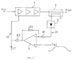
- the transmitter of a known digital radio telephone comprises a voltage controlled RF power amplifier, which is controlled by a control amplifier in accordance with a control logic and the output power of the power amplifier.
- a typical transmitter block diagram of a GSM radio telephone of this kind is shown in figure 1.
- the input square wave pulses Pin are amplified in a desired way and their rise and fall transformed into a cos2-shape in a multi-stage power amplifier 1.
- the output power is measured by a directional coupler 2 and a power sensing element 3, which produces a voltage V1 proportional to the power.
- This voltage is directed to a control amplifier 4, which can be an operational amplifier, and the second input of the control amplifier receives a control pulse TXC from a D/A-converter.
- TXC control pulse
- the amplitude and the rising and falling edge waveforms of the transmit pulse Pout with the desired power are produced with the aid of the control pulse. If the voltage V1 is higher than the voltage TXC, the output voltage of the power amplifier 4 is adjusted lower, whereby the output voltage naturally decreases. Thereby the control loop tries to keep the output pulse shape equal to the control pulse shape.
- control loop's cut-off frequency and open-loop gain which mainly are determined by the components R1, R2, R3 and C1, should be relatively high so that the control loop could keep the pace also when the control pulse TXC is small.
- it is not possible to sufficiently increase the cut-off frequency and the open-loop gain because the control amplifier 4 and the power amplifier 1 exhibit delays which are evident e.g. in the open-loop phase response.
- a control loop designed to be sufficiently rapid is therefore generally unstable, i.e. it oscillates either in a damped way or, in the worst case, undamped.
- Figures 2A and 2B show the voltages Vout ( ⁇ Pout), TXC and the control voltage V2 in a situation, where a pulse begins to rise towards the peak value and where the control loop is stabilized by making it slower, either by decreasing the cut-off frequency or the gain.
- Figure 2A shows a situation at a high power level and figure 2B at a low power level.
- the voltage TXC is scaled to be as high as the output voltage of the power amplifier, although in reality TXC is of course very low.
- V3 is that value of the control voltage V2, at which the power amplifier 1 begins to produce power.
- the output power of the power amplifier starts to rise only at time T4 and it can be seen that the waveform of the output voltage Vout hardly follows the form of the control pulse TXC, as it should.
- the maximum power is achieved at time T2, a moment ⁇ T later than on higher power levels.
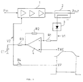
- the basic idea of the invention is that immediately at the beginning of the control pulse TXC the squarewave pulse rapidly increases the value of the control voltage into the proximity of the threshold level V3, at which the power amplifier begins to operate. Then the control loop can operate immediately when the power amplifier starts to produce power. No noticeable delay is thereby created, and the rise at the beginning of the output power Pout is not step-like. Due to the summing of the squarewave pulse and the control voltage a voltage division appears at the power amplifier output, affecting the power amplifier control loop and reducing the open-loop gain. In order to prevent this it is preferred to arrange it so that the squarewave pulse Vp will not be added to the control voltage when the control loop has started to operate. This is arranged with circuitry presented in a preferred embodiment of the invention.
- the output voltage Vs of the control amplifier 4 is added after the resistor R3 to a squarewave pulse Vp having a height approximately the same as the voltage V3, above which the power amplifier 1 begins to produce power.
- the squarewave pulse begins substantially at the same moment when the control pulse TXC begins to rise.
- the capacitor C1 is rapidly charged through the resistor R4 to the proximity of the threshold level V3, and the power amplifier control loop is able to operate immediately when the power amplifier delivers power.
- the control loop will compensate for the effect of the pulse above the level V3 so that the control amplifier 4 output voltage Vs begins to decrease until the influence of the squarewave pulse on the control voltage V2 has been compensated, and thereafter the control voltage continues to rise.
- the arrangement works even if Vp would not exceed the value V3 and then the control amplifier output voltage Vs will not exhibit the mentioned "bend" when V2 exceeds the threshold level.
- Figure 4A shows the corresponding voltage graphs as figure 2A. It is observed, that when a squarewave pulse Vp is added to the control pulse TXC immediately at its beginning at T3, the control voltage V2 will rapidly rise to the value V3 and stay there for a short time, during which the power amplifier and the control loop begin to operate, and then it will begin to rise following the output voltage of the control amplifier 4. The function is the same in figure 4B showing graphs for low power levels. Comparing figures 4A, 4B with figures 2A, 2B it is clearly seen that there is no step-like rise in the power amplifier output voltage Vout when the squarewave pulse is added to the control voltage V2, but the voltage starts to rise without any significant delay, following closely the waveform of TXC and thus the desired cos2-waveform. In a corresponding way the shape of the pulse will keep to the cos2-waveform at the end of the transmission pulse, due to the squarewave pulse Vp.
- the squarewave pulse Vp is added to the control voltage V2 with the aid of a transistor Q1.
- the capacitor C1 is rapidly charged through the resistor R4 and the voltage V2 will rapidly reach the threshold value at which the power amplifier 1 begins to operate, as is mentioned above.
- the control pulse TXC from the control amplifier and through the resistor R3 now continues to rise, the base-emitter voltage of the transistor Q1 will be reduced because the base voltage is constant, i.e. Vp, and the emitter voltage is rising.
- the transistor will cease to conduct when the emitter voltage reaches the base voltage, and the resistor R4 is in a way disconnected from the respective circuit.
- the transistor begins to conduct when the voltage V2 has fallen below the threshold voltage V3, the squarewave pulse V2 being again added to the control voltage, which leads to a controlled shape of the transmission pulse.
- the loop gain is thus not reduced due to the summing circuit and the control loop will operate fast and accurately.
- the resistor R4 may be dimensioned with a much lower value than with the summing circuit alone, with the result that the control voltage V2 can rise to the threshold level V3 with significant speed.
- a base-emitter temperature compensating circuit e.g. in a known way with the diode D1 and resistors R5 and R6.
- the power amplifier transmission pulse is provided with a good cos2-shape and tracking of the control pulse TXC almost without delay, immediately at the beginning of the pulse.
- the presented means is useful at all required power levels.
- the squarewave pulse can be produced e.g. in the logic section of the radio telephone or also with a comparator from the TXC-pulse.
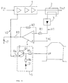
- the invention has been presented as applied to the described control loop in a radio telephone power amplifier, but it is appreciated that it may be applied to control loops realized in other ways.
Applications Claiming Priority (2)
| Application Number | Priority Date | Filing Date | Title |
|---|---|---|---|
| FI896266 | 1989-12-22 | ||
| FI896266A FI87028C (fi) | 1989-12-22 | 1989-12-22 | Metod foer att reglera effekt hos en spaenningsstyrd effektfoerstaerkare och koppling foer anvaendning i metoden |
Publications (3)
| Publication Number | Publication Date |
|---|---|
| EP0434294A2 EP0434294A2 (en) | 1991-06-26 |
| EP0434294A3 EP0434294A3 (en) | 1992-03-04 |
| EP0434294B1 true EP0434294B1 (en) | 1995-08-30 |
Family
ID=8529589
Family Applications (1)
| Application Number | Title | Priority Date | Filing Date |
|---|---|---|---|
| EP90313522A Expired - Lifetime EP0434294B1 (en) | 1989-12-22 | 1990-12-12 | A power control method for a voltage controlled power amplifier and circuitry used in the method |
Country Status (6)
| Country | Link |
|---|---|
| US (1) | US5101175A (fi) |
| EP (1) | EP0434294B1 (fi) |
| JP (1) | JP3045319B2 (fi) |
| AT (1) | ATE127293T1 (fi) |
| DE (1) | DE69022011T2 (fi) |
| FI (1) | FI87028C (fi) |
Families Citing this family (43)
| Publication number | Priority date | Publication date | Assignee | Title |
|---|---|---|---|---|
| DE69112207T2 (de) * | 1990-04-05 | 1996-03-28 | Roberto Crea | "walk-through"-mutagenese. |
| CA2044672C (en) * | 1990-06-16 | 1994-10-04 | Hidehiko Norimatsu | Burst control circuit for use in tdma communications system |
| GB2247793A (en) * | 1990-09-06 | 1992-03-11 | Motorola Inc | Control of pulse power amplifier rise and fall |
| GB9105064D0 (en) * | 1991-03-11 | 1991-04-24 | Philips Electronic Associated | Power amplifier and transmitting apparatus including such a power amplifier |
| US5150075A (en) * | 1991-06-03 | 1992-09-22 | Motorola, Inc. | Power amplifier ramp up method and apparatus |
| TW225619B (fi) * | 1991-07-19 | 1994-06-21 | Nippon Electric Co | |
| JPH0590853A (ja) * | 1991-09-27 | 1993-04-09 | Nec Corp | 電力増幅回路 |
| FI95853C (fi) * | 1991-11-08 | 1996-03-25 | Nokia Mobile Phones Ltd | Menetelmä D/A-muuntimen offset-jännitteiden vaihteluiden vaikutuksen korjaamiseksi muuntimen lähtöjännitteestä |
| FI91201C (fi) * | 1992-06-05 | 1994-05-25 | Nokia Mobile Phones Ltd | Boosteri |
| GB9213996D0 (en) * | 1992-07-01 | 1992-08-12 | Shaye Communications Ltd | Method and apparatus for controlling amplifier power |
| GB9219825D0 (en) * | 1992-09-18 | 1992-10-28 | Philips Electronics Uk Ltd | Power amplifier and a transmitter including the power amplifier |
| FI93159C (fi) * | 1992-09-23 | 1995-02-27 | Nokia Mobile Phones Ltd | Menetelmä radiopuhelimen radiotaajuusvahvistimen ohjaamiseksi ja menetelmän mukainen ohjausjärjestelmä |
| JPH06334541A (ja) * | 1993-05-25 | 1994-12-02 | Sony Corp | 無線送信機 |
| FI97179C (fi) * | 1994-06-15 | 1996-10-25 | Nokia Mobile Phones Ltd | Pulssitetun lähettimen lähtötehon säätö ja tehon verhokäyrän muotoilu |
| JP2571033B2 (ja) * | 1994-12-30 | 1997-01-16 | 日本電気株式会社 | 送信電力増幅回路の出力制御回路 |
| FI101505B1 (fi) * | 1995-05-10 | 1998-06-30 | Nokia Mobile Phones Ltd | Menetelmä suuntakytkimellä toteutetun tehonmittauksen parantamiseksi pienillä tehotasoilla |
| JPH09205333A (ja) * | 1996-01-24 | 1997-08-05 | Sony Corp | 電力増幅回路 |
| JPH09238037A (ja) * | 1996-03-01 | 1997-09-09 | Nec Corp | 出力電力制御回路 |
| US5710697A (en) * | 1996-03-26 | 1998-01-20 | Unitrode Corporation | Power supply controller having frequency foldback and volt-second duty cycle clamp features |
| US5752172A (en) * | 1996-08-16 | 1998-05-12 | Nokia Mobile Phones Limited | Distributed transmitter output power control circuit and method for a radio telephone |
| FI963389A (fi) * | 1996-08-30 | 1998-03-01 | Nokia Mobile Phones Ltd | Käsipuhelimen opastusjärjestelmä |
| FI106759B (fi) | 1996-11-13 | 2001-03-30 | Nokia Mobile Phones Ltd | Matkaviestimen lähetystehon rajoitinjärjestelmä |
| US6173160B1 (en) | 1996-11-18 | 2001-01-09 | Nokia Mobile Phones Limited | Mobile station having drift-free pulsed power detection method and apparatus |
| FI108177B (fi) | 1997-01-03 | 2001-11-30 | Nokia Mobile Phones Ltd | Matkaviestinlaitteiden lähetin |
| US5884149A (en) * | 1997-02-13 | 1999-03-16 | Nokia Mobile Phones Limited | Mobile station having dual band RF detector and gain control |
| DE19705735A1 (de) * | 1997-02-14 | 1998-08-20 | Nokia Mobile Phones Ltd | Verfahren und Vorrichtung zur Inspektion wenigstens eines Antennenzweigs, insbesondere in einem Fahrzeug |
| GB2330960A (en) * | 1997-10-29 | 1999-05-05 | Nokia Telecommunications Oy | Feedback rf power control with offset stored during off period removed during on period |
| FI105611B (fi) * | 1998-03-13 | 2000-09-15 | Nokia Mobile Phones Ltd | Radiotajuusvahvistimet |
| GB9811382D0 (en) | 1998-05-27 | 1998-07-22 | Nokia Mobile Phones Ltd | A transmitter |
| GB9811381D0 (en) | 1998-05-27 | 1998-07-22 | Nokia Mobile Phones Ltd | Predistortion control for power reduction |
| GB2339113B (en) | 1998-06-30 | 2003-05-21 | Nokia Mobile Phones Ltd | Data transmission in tdma system |
| US6169886B1 (en) * | 1998-11-02 | 2001-01-02 | Motorola, Inc. | Power amplifier control according to a delayed waveform suitable for use in a communication device |
| DE50000699D1 (de) * | 1999-02-11 | 2002-12-05 | Siemens Ag | Verfahren und anordnung zur leistungsregelung eines sendeverstärkers |
| EP1094600A1 (en) * | 1999-10-19 | 2001-04-25 | Siemens Aktiengesellschaft | Apparatus for amplifying signals |
| US6721368B1 (en) * | 2000-03-04 | 2004-04-13 | Qualcomm Incorporated | Transmitter architectures for communications systems |
| US6292122B1 (en) * | 2000-03-04 | 2001-09-18 | Qualcomm, Incorporated | Digital-to-analog interface circuit having adjustable time response |
| JP2005503118A (ja) * | 2001-02-14 | 2005-02-03 | ジェンザイム・コーポレーション | 改変ペプチドリガンド |
| US6404284B1 (en) | 2001-04-19 | 2002-06-11 | Anadigics, Inc. | Amplifier bias adjustment circuit to maintain high-output third-order intermodulation distortion performance |
| US20020155817A1 (en) * | 2001-04-20 | 2002-10-24 | Per-Olof Brandt | Regulation for saturated systems |
| FR2824433B1 (fr) * | 2001-05-07 | 2003-08-01 | Cit Alcatel | Dispositif de regulation du controle de la puissance d'un emetteur |
| JP3928421B2 (ja) * | 2001-12-13 | 2007-06-13 | 三菱電機株式会社 | 送信出力の制御装置及び制御方法 |
| US7768353B2 (en) * | 2008-06-13 | 2010-08-03 | Samsung Electro-Mechanics Company, Ltd. | Systems and methods for switching mode power amplifier control |
| SG11201405848UA (en) | 2012-03-23 | 2014-10-30 | Univ Queensland | Immunomodulatory agent and uses therefor |
Family Cites Families (4)
| Publication number | Priority date | Publication date | Assignee | Title |
|---|---|---|---|---|
| JPS5999851A (ja) * | 1982-11-29 | 1984-06-08 | Nec Corp | 信号制御回路 |
| JPS6041821A (ja) * | 1983-08-18 | 1985-03-05 | Nec Corp | 送信出力電力制御装置 |
| US4706262A (en) * | 1984-03-30 | 1987-11-10 | Nec Corporation | FSK or FM burst signal generating apparatus |
| JP2667388B2 (ja) * | 1986-02-28 | 1997-10-27 | 株式会社東芝 | 自動電力制御装置 |
-
1989
- 1989-12-22 FI FI896266A patent/FI87028C/fi not_active IP Right Cessation
-
1990
- 1990-12-12 EP EP90313522A patent/EP0434294B1/en not_active Expired - Lifetime
- 1990-12-12 AT AT90313522T patent/ATE127293T1/de active
- 1990-12-12 DE DE69022011T patent/DE69022011T2/de not_active Expired - Fee Related
- 1990-12-14 US US07/627,810 patent/US5101175A/en not_active Expired - Lifetime
- 1990-12-25 JP JP2405875A patent/JP3045319B2/ja not_active Expired - Fee Related
Also Published As
| Publication number | Publication date |
|---|---|
| FI896266A0 (fi) | 1989-12-22 |
| JP3045319B2 (ja) | 2000-05-29 |
| EP0434294A3 (en) | 1992-03-04 |
| US5101175A (en) | 1992-03-31 |
| FI87028B (fi) | 1992-07-31 |
| DE69022011T2 (de) | 1996-04-11 |
| EP0434294A2 (en) | 1991-06-26 |
| ATE127293T1 (de) | 1995-09-15 |
| DE69022011D1 (de) | 1995-10-05 |
| FI896266A (fi) | 1991-06-23 |
| FI87028C (fi) | 1992-11-10 |
| JPH03289805A (ja) | 1991-12-19 |
Similar Documents
| Publication | Publication Date | Title |
|---|---|---|
| EP0434294B1 (en) | A power control method for a voltage controlled power amplifier and circuitry used in the method | |
| KR960000351B1 (ko) | 고주파 송신 장치의 출력 레벨 제어 회로 | |
| US4360787A (en) | Digitally controlled wide ranch automatic gain control | |
| FI105510B (fi) | Säätöpiiri ja menetelmä lähetyslähtöön | |
| US5128629A (en) | Method for controlling the output power of digital cellular telephones | |
| US4560949A (en) | High speed AGC circuit | |
| EP0786859B1 (en) | Power amplifying circuit and method | |
| JP2924644B2 (ja) | 送信電力制御回路、基地局、移動機及び移動体通信システム | |
| EP0547078B1 (en) | Power amplifier | |
| EP0554097A1 (en) | Control device for power amplifier | |
| CN101167240A (zh) | 切换式电源调节 | |
| EP0541351A2 (en) | D/A converter offset correction | |
| US6445168B2 (en) | Power output circuit having a pulse-width modulation mode and a permanently closed mode | |
| EP0034510B1 (en) | Improvements in or relating to pulsed solid state systems | |
| JP3022364B2 (ja) | 送信出力制御回路 | |
| US4900988A (en) | High voltage stabilizing circuit for preventing overheat | |
| JP2973717B2 (ja) | 高周波送信装置の出力レベル制御回路 | |
| GB2059202A (en) | Digitally controlled wide range automatic gain control | |
| KR960007571B1 (ko) | 교환기 가입자회로에 있어서 스위칭 레귤레이터 | |
| JPS6451703A (en) | Oscillation circuit | |
| KR0136655Y1 (ko) | 다중모드 모니터의 수평사이즈 가변범위 보정회로 | |
| SU1656508A1 (ru) | Способ управлени импульсным стабилизатором посто нного напр жени | |
| KR100317212B1 (ko) | 자동전압레벨제어회로 | |
| EP1137173A1 (en) | RF- FET bias and switching circuit based on a quasi-open loop regulation | |
| JPH04155982A (ja) | 光出力安定化方式 |
Legal Events
| Date | Code | Title | Description |
|---|---|---|---|
| PUAI | Public reference made under article 153(3) epc to a published international application that has entered the european phase |
Free format text: ORIGINAL CODE: 0009012 |
|
| AK | Designated contracting states |
Kind code of ref document: A2 Designated state(s): AT BE CH DE DK ES FR GB GR IT LI LU NL SE |
|
| PUAL | Search report despatched |
Free format text: ORIGINAL CODE: 0009013 |
|
| AK | Designated contracting states |
Kind code of ref document: A3 Designated state(s): AT BE CH DE DK ES FR GB GR IT LI LU NL SE |
|
| 17P | Request for examination filed |
Effective date: 19920827 |
|
| 17Q | First examination report despatched |
Effective date: 19941102 |
|
| GRAA | (expected) grant |
Free format text: ORIGINAL CODE: 0009210 |
|
| AK | Designated contracting states |
Kind code of ref document: B1 Designated state(s): AT BE CH DE DK ES FR GB GR IT LI LU NL SE |
|
| PG25 | Lapsed in a contracting state [announced via postgrant information from national office to epo] |
Ref country code: GR Free format text: LAPSE BECAUSE OF FAILURE TO SUBMIT A TRANSLATION OF THE DESCRIPTION OR TO PAY THE FEE WITHIN THE PRESCRIBED TIME-LIMIT Effective date: 19950830 Ref country code: ES Free format text: THE PATENT HAS BEEN ANNULLED BY A DECISION OF A NATIONAL AUTHORITY Effective date: 19950830 Ref country code: DK Effective date: 19950830 Ref country code: BE Effective date: 19950830 Ref country code: AT Effective date: 19950830 |
|
| REF | Corresponds to: |
Ref document number: 127293 Country of ref document: AT Date of ref document: 19950915 Kind code of ref document: T |
|
| ET | Fr: translation filed | ||
| REF | Corresponds to: |
Ref document number: 69022011 Country of ref document: DE Date of ref document: 19951005 |
|
| ITF | It: translation for a ep patent filed |
Owner name: MODIANO & ASSOCIATI S.R.L. |
|
| PG25 | Lapsed in a contracting state [announced via postgrant information from national office to epo] |
Ref country code: LU Free format text: LAPSE BECAUSE OF NON-PAYMENT OF DUE FEES Effective date: 19951231 |
|
| PLBE | No opposition filed within time limit |
Free format text: ORIGINAL CODE: 0009261 |
|
| STAA | Information on the status of an ep patent application or granted ep patent |
Free format text: STATUS: NO OPPOSITION FILED WITHIN TIME LIMIT |
|
| 26N | No opposition filed | ||
| REG | Reference to a national code |
Ref country code: GB Ref legal event code: IF02 |
|
| PGFP | Annual fee paid to national office [announced via postgrant information from national office to epo] |
Ref country code: CH Payment date: 20020104 Year of fee payment: 12 |
|
| REG | Reference to a national code |
Ref country code: GB Ref legal event code: 732E |
|
| PGFP | Annual fee paid to national office [announced via postgrant information from national office to epo] |
Ref country code: SE Payment date: 20021204 Year of fee payment: 13 |
|
| PG25 | Lapsed in a contracting state [announced via postgrant information from national office to epo] |
Ref country code: LI Free format text: LAPSE BECAUSE OF NON-PAYMENT OF DUE FEES Effective date: 20021231 Ref country code: CH Free format text: LAPSE BECAUSE OF NON-PAYMENT OF DUE FEES Effective date: 20021231 |
|
| REG | Reference to a national code |
Ref country code: CH Ref legal event code: PL |
|
| PGFP | Annual fee paid to national office [announced via postgrant information from national office to epo] |
Ref country code: NL Payment date: 20031205 Year of fee payment: 14 |
|
| PGFP | Annual fee paid to national office [announced via postgrant information from national office to epo] |
Ref country code: GB Payment date: 20031210 Year of fee payment: 14 Ref country code: FR Payment date: 20031210 Year of fee payment: 14 |
|
| PG25 | Lapsed in a contracting state [announced via postgrant information from national office to epo] |
Ref country code: SE Free format text: LAPSE BECAUSE OF NON-PAYMENT OF DUE FEES Effective date: 20031213 |
|
| PGFP | Annual fee paid to national office [announced via postgrant information from national office to epo] |
Ref country code: DE Payment date: 20031229 Year of fee payment: 14 |
|
| EUG | Se: european patent has lapsed | ||
| PG25 | Lapsed in a contracting state [announced via postgrant information from national office to epo] |
Ref country code: GB Free format text: LAPSE BECAUSE OF NON-PAYMENT OF DUE FEES Effective date: 20041212 |
|
| PG25 | Lapsed in a contracting state [announced via postgrant information from national office to epo] |
Ref country code: NL Free format text: LAPSE BECAUSE OF NON-PAYMENT OF DUE FEES Effective date: 20050701 Ref country code: DE Free format text: LAPSE BECAUSE OF NON-PAYMENT OF DUE FEES Effective date: 20050701 |
|
| GBPC | Gb: european patent ceased through non-payment of renewal fee |
Effective date: 20041212 |
|
| PG25 | Lapsed in a contracting state [announced via postgrant information from national office to epo] |
Ref country code: FR Free format text: LAPSE BECAUSE OF NON-PAYMENT OF DUE FEES Effective date: 20050831 |
|
| NLV4 | Nl: lapsed or anulled due to non-payment of the annual fee |
Effective date: 20050701 |
|
| REG | Reference to a national code |
Ref country code: FR Ref legal event code: ST |
|
| PG25 | Lapsed in a contracting state [announced via postgrant information from national office to epo] |
Ref country code: IT Free format text: LAPSE BECAUSE OF NON-PAYMENT OF DUE FEES Effective date: 20051212 |