EP0417801A2 - Appareil de formation d'images comprenant des moyens de chargement - Google Patents
Appareil de formation d'images comprenant des moyens de chargement Download PDFInfo
- Publication number
- EP0417801A2 EP0417801A2 EP90117691A EP90117691A EP0417801A2 EP 0417801 A2 EP0417801 A2 EP 0417801A2 EP 90117691 A EP90117691 A EP 90117691A EP 90117691 A EP90117691 A EP 90117691A EP 0417801 A2 EP0417801 A2 EP 0417801A2
- Authority
- EP
- European Patent Office
- Prior art keywords
- image
- bearing member
- image bearing
- voltage
- charging
- Prior art date
- Legal status (The legal status is an assumption and is not a legal conclusion. Google has not performed a legal analysis and makes no representation as to the accuracy of the status listed.)
- Granted
Links
Images


Classifications
-
- G—PHYSICS
- G03—PHOTOGRAPHY; CINEMATOGRAPHY; ANALOGOUS TECHNIQUES USING WAVES OTHER THAN OPTICAL WAVES; ELECTROGRAPHY; HOLOGRAPHY
- G03G—ELECTROGRAPHY; ELECTROPHOTOGRAPHY; MAGNETOGRAPHY
- G03G15/00—Apparatus for electrographic processes using a charge pattern
- G03G15/02—Apparatus for electrographic processes using a charge pattern for laying down a uniform charge, e.g. for sensitising; Corona discharge devices
- G03G15/0208—Apparatus for electrographic processes using a charge pattern for laying down a uniform charge, e.g. for sensitising; Corona discharge devices by contact, friction or induction, e.g. liquid charging apparatus
- G03G15/0216—Apparatus for electrographic processes using a charge pattern for laying down a uniform charge, e.g. for sensitising; Corona discharge devices by contact, friction or induction, e.g. liquid charging apparatus by bringing a charging member into contact with the member to be charged, e.g. roller, brush chargers
-
- Y—GENERAL TAGGING OF NEW TECHNOLOGICAL DEVELOPMENTS; GENERAL TAGGING OF CROSS-SECTIONAL TECHNOLOGIES SPANNING OVER SEVERAL SECTIONS OF THE IPC; TECHNICAL SUBJECTS COVERED BY FORMER USPC CROSS-REFERENCE ART COLLECTIONS [XRACs] AND DIGESTS
- Y10—TECHNICAL SUBJECTS COVERED BY FORMER USPC
- Y10S—TECHNICAL SUBJECTS COVERED BY FORMER USPC CROSS-REFERENCE ART COLLECTIONS [XRACs] AND DIGESTS
- Y10S347/00—Incremental printing of symbolic information
- Y10S347/90—Data processing for electrostatic recording
Definitions
- the present invention relates to an image forming apparatus such as a laser beam printer, wherein an image bearing member is electrically charged by a charging member contacted to the image bearing member and supplied with a vibratory voltage, and the charged surface of the image bearing member is scanned line by line to be exposed to image information.
- Contact charging is the charging in which a charging member supplied with a voltage is contacted to a member to be charged to apply electric charge to the member to be charged to a desired potential level.
- the voltage required for providing the potential level on the member to be charged is smaller; the quantity of ozone produced by the charging action is very small so that the ozone removing filter is not required, and the air discharging system is simplified; the maintenance operation is easy; and the structure is simple.
- a member 1 is to be charged, and is an electrophotographic photosensitive member or an electrostatic recording dielectric member, which will hereinafter be called simply "photosensitive drum", in the form of a drum rotatable at a predetermined peripheral speed (process speed) in a direction indicated by an arrow, for example.
- photosensitive drum in the form of a drum rotatable at a predetermined peripheral speed (process speed) in a direction indicated by an arrow, for example.
- a contact charging member 2 is in the form of a conductive roller (charging roller) and comprises a core metal 2b and conductive roller 2a therearound made of conductive rubber or the like.
- the charging roller 2 is press-contacted to the surface of the photosensitive drum with a predetermined pressure provided by urging springs 10 acting on the opposite end portions of the core metal 2b.
- the conductive roller rotates following rotation of the photosensitive drum 1.
- a voltage application source 9 applies a voltage to the charging roller 2 by way of a contact leaf spring 8 contacted to the core metal 2b of the charging roller 2.
- the voltage is a vibratory voltage (DC biased AC voltage) having a peak-to-peak voltage Vpp larger than twice a charge starting voltage relative to the photosensitive member.
- the contact charging member is not limit to a roller configuration, but may be in the form of a blade, a rod, a block, a pad, a belt, a web, a brush or the like.
- the image forming apparatus using the contact type charging means supplied with such a voltage so as to charge the image bearing member involves the following problems.
- Figure 5 shows an example of horizontal line pattern image 11a formed on a recording sheet 11.
- the image may have interference stripes 11b if the spatial frequency by the frequency of the voltage source 9 to the contact charging member 2 becomes close to the intervals between the horizontal lines 11a.
- the frequency of the voltage source 9 can vary ⁇ 10 % from the rated frequency because of parts error. With some voltage source 9, the spatial frequency thereof is the same as the intervals between horizontal lines 11a with the result of remarkable interference stripes 11b.
- the image forming apparatus is a laser beam printer using an electrophotographic process wherein a contact type charger is used to charge an image bearing member 1.
- the image bearing member is an electrophotographic photosensitive member (photosensitive drum) in the form of a rotatable drum.
- photosensitive drum in the form of a rotatable drum.
- it comprises an aluminum base drum 1b coated with a photosensitive layer of organic photoconductor (OPC) 1a.
- OPC organic photoconductor
- the outer diameter thereof is 30 mm and is rotated at a predetermined process speed Vp (peripheral speed) in the clockwise direction A.
- Vp peripheral speed
- the drum base 1b is electrically grounded.
- a contact type charging member 2 is in the form of a charging roller and comprises a core metal 2b covered with conductive roller 2a having elasticity and made of carbon-dispersed EPDM or urethane or the like. Similarly to the case of Figure 4, the opposite end portions of the core metal shaft 2b are urged by urging springs toward the photosensitive drum 1 surface to press-contact the charging member thereto. The charging roller rotates following rotation of the photosensitive drum 1.
- the charging roller 2 is provided with a resistance layer on the conductive roller 2a to prevent leakage to the photosensitive drum 1, the resistance layer being made of epichlorohydrin rubber having a larger volume, resistivity than the conductive roller 2a, and further, the resistance layer is coated with resin layer to prevent softening agent contained in the rubber, the resin layer being made of N methoxy methyl nylon. Although, these layers are not shown in the Figure, but it is preferable that they are provided.
- the charging roller 2 is supplied by way of the contact leaf spring 8 with a vibratory voltage, that is, a DC biased AC voltage having a frequency f (Vdc + Vac) to form an alternating electric field between the charging roller 2 and the photosensitive drum 1, by which the surface of the rotating photosensitive drum 1 is uniformly charged to a predetermined negative potential.
- a vibratory voltage that is, a DC biased AC voltage having a frequency f (Vdc + Vac) to form an alternating electric field between the charging roller 2 and the photosensitive drum 1, by which the surface of the rotating photosensitive drum 1 is uniformly charged to a predetermined negative potential.
- a laser beam scanner 3 is supplied with time series electric digital signals corresponding to picture elements representing an intended image from a host apparatus (not shown) such as a computer, a wordprocessor or an image reader. It emits a laser beam L imagewisely modulated at a predetermined printing density D (dpi) in accordance with the digital picture element signal.
- the surface of the photosensitive drum 1 electrically charged in the manner described above, is exposed to the laser beam L from the scanner 3 controlled by the controller, so that the drum is scanned by the laser beam L in the main scan direction, that is, in the direction parallel to the generating line of the photosensitive drum. By repeating this, an electrostatic latent image corresponding to the intended image information is formed on the photosensitive drum 1 surface.
- the latent image is developed by a developing sleeve 4 of the developing device, more particularly, the portion of the photosensitive drum 1 having been exposed to the laser beam L receives negatively charged toner.
- the developed image is transferred onto a transfer material 7 made of paper and introduced from an unshown sheet feeding station at a proper timing with the developed image to an image transfer station where the photosensitive drum 1 and the transfer roller 5 supplied with a positive DC voltage are contacted or faced.
- the transfer material 7 having passed through the transfer station is separated from the photosensitive drum and is conveyed to an unshown image fixing station.
- the surface of the photosensitive drum 1, from which the image has been transferred, is cleaned by a cleaning blade 6, so that the residual toner or other contamination matter is removed to be prepared for the next image forming operation.
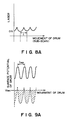
- Figures 8A, 8B and 8C show the projections of the laser beam on the moving photosensitive drum.
- the intervals between adjacent scanning lines are indicated by 1 .
- the laser beam emitted from the laser scanner is reflected by one of rotating polygonal mirror surfaces to line scan once the photosensitive drum in the main scan direction.
- the printing density by the laser scanning line is assumed as being 200 dpi (dot per inch).
- the spatial wavelength ⁇ sp of the cycle pattern varies more or less depending on the variation of the frequency and the variation in the process speed. It can be measured in the following manner. First, the photosensitive drum is uniformly charged by the charging roller, and then, is exposed to uniform light at its whole surface. The amount of exposure is adjusted so that the cycle pattern on the photosensitive drum is clearly developed.
- the developed cycle pattern is transferred and fixed on the transfer sheet.
- the cycle pattern on the transfer sheet is measured using a magnifier, so that the variations of the spatial wavelength ⁇ sp is measured.
- the cycle pattern becomes smaller with increase of the frequency f of the AC component of the voltage source 9. If it is equal to or larger than several thousand hertz, for example, the pattern is hardly observable by human eyes.
- the frequency f is higher than 600 Hz, the charging roller mechanically vibrates relative to the photosensitive drum, with the result of noise, and therefore, the frequency f is preferably not more than 600 Hz.
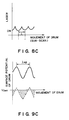
- Figure 9A is a graph of the surface potential of the photosensitive drum vs. positions of the moving photosensitive drum surface.
- the surface of the charging roller is contaminated with foreign matter such as toner particles, silica particles, paper dust or the like, and if this occurs, the contamination portion has come to have electrostatic capacity.
- the interference stripes 11b may occur as shown in Figure 5.
- the phase of the charging potential is deviated from that of Figure 9A by the amount of half wavelength, for example, that is, if the interval 1 between adjacent scanning lines and the phase of the spatial wavelength ⁇ sp are deviated, the whole surface of the photosensitive drum receives the toner with the developing bias of VDev, as shown in Figures 8B and 10B.
- the interference stripes appear as shown in Figure 9A, or do not appear as in Figure 9B, depending on the difference of the foreign matter (difference in the electrostatic capacity) along the length of the charging roller.
- the interference stripes are produced depending on the developing bias level if the spatial wavelength is an integer multiple (double in Figure 9C) or an integer reciprocal of the interval between adjacent scanning lines.
- the spatial wavelength ⁇ sp is not determined only on the frequency f of the voltage source, but is dependent on the process speed Vp, and therefore, the variation in the process speed Vp is considered similarly as the variation in the spatial wavelength ⁇ sp as discussed above.
- the condition of not producing the interference stripes is that the variation range of the wavelengths ⁇ sp does not contain an integer multiple or a reciprocal of an integer multiple of the diameter d.
- the frequency f of the vibratory voltage provided by the voltage source 9, and the process speed Vp are so determined that the range of the spatial wavelength ⁇ sp with its variation and the interval 1 between adjacent scanning lines multiplied by n or 1/n (n: integer) are not overlapped.
- the interference stripes attributable to the interference between the spatial wavelength ⁇ sp and the scanning line interval can be prevented.
- the laser beam printer described above is capable of forming line images of various patterns.
- the interference stripes are prevented from occurring in any line image patterns.
- the laser beam printer various pattern of line images can be formed.
- the laser beam printer is adjustable so that the numbers n and m are arbitrary.
- Figure 6A shows an example of on and off of the laser beam. It is a graph of laser on/off vs. the position on the moving image bearing member. During the laser beam being on, the laser beam scans one line on the surface of the photosensitive drum in the main scan detection by one reflecting surface of the rotating polygonal mirror.
- n dots and m species means that the laser beam scans (on) n lines, and thereafter the laser does not scan (off) m lines, and these operations are repeated.
- the contact charging as contrasted to corona charging, the charge distance G ( Figure 4) is very short, more particularly, as short as approximately 30 microns, and therefore, the charging action is easily influenced by the voltage source 9.
- the spatial wavelength ⁇ sp of the cycle pattern varies slightly because of the variations in the frequency and the process speed.
- the range of the variation can be determined by observing the cycle pattern formed on a transfer sheet, in the manner described in the foregoing.
- Figure 7A is a graph of the surface potential of the photosensitive drum vs. position of the moving surface of the photosensitive drum.
- the phases thereof becomes the same the falling of the potential across the developing bias vDep becomes large as shown in Figure 7A, with the result that the lines are developed thick, and therefore, interference stripes are produced.
- the phase difference between the wavelength of (n+m)d and the spatial wavelength ⁇ sp is the half wavelength, as shown in Figures 6B and 7B, the lines are developed thin, and the interference stripes are produced.
- the surface potential induced on the photosensitive drum 1 is different in the phase between the portion having the electrostatic capacity and the portion not having the capacity.
- Figure 10 is a graph of a spatial wavelength ⁇ sp vs. voltage source frequency f under the condition that the process speed Vp is 12 ⁇ mm/sec, and the printing density is 400 dpi.
- (n+m)d of the horizontal line pattern with one dot and one space is 127.0 microns
- (n+m)d of the horizontal line pattern with 1 dot and 2 spaces is 190.5 microns
- (n+m)d of the horizontal line pattern with 1 dot and 3 spaces is 254.0 microns.
- the rated frequency of the voltage source was 290 Hz, and the variation of the frequency due to the accuracy of the parts or the like was 10 %, that is, the frequency was 290 ⁇ 10 %, more particularly, the frequency ranges from 261 - 319 Hz.
- the range is indicated by A in Figure 10.
- an integer multiple (one) of (n+m)d may be equal to the spatial wavelength in the range, and therefore, the likelihood of the interference stripe 11b production is high.
- the frequency f of the voltage source When the frequency f of the voltage source is set to be 250 Hz, the actual frequency ranges from 250 Hz + 10 % to 250 Hz - 10 % (225 - 275 Hz, as shown in Figure 10 by B.
- the process speed Vp 12 ⁇ mm/sec
- the spatial wavelength changes within the range from 137 - 168 microns.
- any of the horizontal line patterns with 1 dot and 1 space, with 1 dot and 2 spaces or with 1 dot and 3 spaces do not result in that (n+m)d multiplied by N or by 1/N (N: integer) falls in the variable range of the spatial wavelength.
- N integer
- the frequency f of the voltage source is 210 Hz
- the frequency is in the range of 210 Hz ⁇ 10 %, as indicated by a reference C in Figure 10 (189 - 231 Hz).
- the process speed Vp 12 ⁇ mm/sec
- the spatial wavelength varies from 163 - 199 microns.
- (n+m)d 190.5 microns falls in the variable range of the spatial wavelength. Therefore, when the frequency f and the process speed Vp are set in this manner, the likelihood of the interference stripe production is high.
- the interference stripes are produced if the spatial wavelength is an integer multiple or a reciprocal of an integer of (n+m)d.
- the wavelength of the horizontal line pattern is an integer of the diameter of dot, and therefore, the non-interference-stripe condition is satisfied if the variable range of ⁇ sp does not contain an integer multiple of the dot diameter of a reciprocal of an integer multiplied by the dot diameter.
- the ranges for the frequency f of the AC component of the voltage source 9 and the process speed Vp is set such that the variable range of the spatial wavelength ⁇ sp does not overlap the range of (n+m)d.
- the interference stripes resulting from the overlapping between the spatial wavelength ⁇ sp and the wavelength of the horizontal line pattern can be removed for any of horizontal line patterns.
- the member to be charged by the charging roller 2 might have a defect such as pin hole or the like. If such a member is charged, using the charging roller 2, it is possible that unusual electric discharge occurs such as electric current leakage. In order to avoid this, the surface of the charging roller is coated with protection layer, as described hereinbefore.
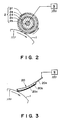
- Figure 2 shows an example of such a charging roller. It comprises a core metal 2b, a low resistance layer may be EPDM or urethane rubber in which carbon is dispersed, a conductive layer 2d made of N methoxy methyl nylon or Torezin (trade name) in which large amount of carbon is dispersed, a high resistance layer 2e made of epichlorohydrin rubber or the like, and a protection layer 2f of Torezin.
- a charging roller 2 is used.
- the contact type charging member is not limited to the roller type, but may be in the form of a blade, a rod, a block, a pad, a belt, a web, a brush or the like.
- FIG. 3 shows an example of a blade type charging member 20 (charging blade). It comprises a sheet metal for applying a bias voltage to the blade, a blade body having a low resistance made of EPDM in which carbon is dispersed, and a high resistance layer 20c of epichlorohydrin rubber.
- the edge of the charging blade 20 is press-contacted to the photosensitive drum 1 counter directionally with respect to movement direction of the surface of the photosensitive drum 1 with a predetermined pressure.
- the charging blade 20 has an advantage over the charging roller in that the cost is low, and the required space is small.
- the present invention is not limited to this, but is applicable to the case wherein an LED head having LED elements arranged along a length of the photosensitive member is faced to the photosensitive member, and the LED are selectively actuated by signals from controller to form a latent image along the scanning line of the group of the LED element.
- the image bearing member is not limited to the photosensitive member but may be an insulating member.
- a multi-stylus recording head may be used which has electrode pins arranged along the length of the image bearing member and faced thereto downstream of the contact charging member with respect to movement detection of the image bearing member.
- the latent image is formed along the line of the multi-stylus pins after the insulating member is electrically charged.
- the present invention is applicable not only to the reverse-development type described in the foregoing, but is usable also to a regular development type.
- the vibratory voltage applied between the image bearing member and the contact type charging member may be a sine wave, rectangular wave or triangular wave.
- the frequency of the vibratory voltage applied between the contact type charging member and the image bearing member and the moving speed of the image bearing member are selected in the ranges described in the foregoing, by which the interference stripes appearing on the output image can be prevented.
- An image forming apparatus includes a movable image bearing member; a charger for charging the image bearing member while it is moving, the charger including a contact member contactable to the image bearing member and voltage source for applying a vibratory voltage between the contact member and the image bearing member; a latent image forming device for forming a latent image along a scanning line on the image bearing member charged by the charger, the latent image being developed and transferred onto a transfer material; wherein a frequency f of the vibratory voltage and a speed Vp of the movement of the image bearing member are so selected that an interval (microns) between adjacent scanning lines multiplies by N or 1/N (N: integer) does not fall of a spatial wavelength ⁇ sp (microns) which is variable.
Landscapes
- Physics & Mathematics (AREA)
- Engineering & Computer Science (AREA)
- Plasma & Fusion (AREA)
- General Physics & Mathematics (AREA)
- Electrostatic Charge, Transfer And Separation In Electrography (AREA)
- Printers Or Recording Devices Using Electromagnetic And Radiation Means (AREA)
Applications Claiming Priority (2)
| Application Number | Priority Date | Filing Date | Title |
|---|---|---|---|
| JP1239562A JPH0789249B2 (ja) | 1989-09-14 | 1989-09-14 | 画像形成装置 |
| JP239562/89 | 1989-09-14 |
Publications (3)
| Publication Number | Publication Date |
|---|---|
| EP0417801A2 true EP0417801A2 (fr) | 1991-03-20 |
| EP0417801A3 EP0417801A3 (en) | 1992-08-26 |
| EP0417801B1 EP0417801B1 (fr) | 1995-04-26 |
Family
ID=17046647
Family Applications (1)
| Application Number | Title | Priority Date | Filing Date |
|---|---|---|---|
| EP90117691A Expired - Lifetime EP0417801B1 (fr) | 1989-09-14 | 1990-09-13 | Appareil de formation d'images comprenant des moyens de chargement |
Country Status (6)
| Country | Link |
|---|---|
| US (1) | US5146281A (fr) |
| EP (1) | EP0417801B1 (fr) |
| JP (1) | JPH0789249B2 (fr) |
| DE (1) | DE69018907T2 (fr) |
| FR (1) | FR2651901B1 (fr) |
| IT (1) | IT1244127B (fr) |
Cited By (9)
| Publication number | Priority date | Publication date | Assignee | Title |
|---|---|---|---|---|
| EP0526208A1 (fr) * | 1991-07-31 | 1993-02-03 | Canon Kabushiki Kaisha | Elément photosensible et appareil électrophotographique l'utilisant |
| EP0572738A1 (fr) * | 1992-05-29 | 1993-12-08 | Canon Kabushiki Kaisha | Dispositif de chargement, appareil de formation d'images et unité de traitement montée de manière amovible dans cet appareil |
| EP0594140A2 (fr) * | 1992-10-19 | 1994-04-27 | SHARP Corporation | Méthode de chargement électrophotographique |
| EP0606907A1 (fr) * | 1993-01-13 | 1994-07-20 | Ricoh Company, Ltd | Rouleau de chargement pour un appareil de formation d'images |
| EP0631205A2 (fr) * | 1993-06-24 | 1994-12-28 | Tokai Rubber Industries, Ltd. | Rouleau électriquement conducteur dont la couche de base est constituée d'un matériau élastique conducteur d'ions |
| EP0661606A3 (fr) * | 1993-12-28 | 1996-02-21 | Matsushita Electric Ind Co Ltd | Dispositif de chargement et un appareil de formation d'images avec le dispositif de chargement. |
| US5786091A (en) * | 1991-12-02 | 1998-07-28 | Ricoh Company, Ltd. | Charge roller for an image forming apparatus |
| EP0890885A2 (fr) * | 1997-07-11 | 1999-01-13 | Sharp Kabushiki Kaisha | Appareil de formation d'images |
| US6190295B1 (en) | 1998-02-24 | 2001-02-20 | Tokai Rubber Industries, Ltd. | Charging roll whose resistance adjusting layer contains insulating particles dispersed therein |
Families Citing this family (16)
| Publication number | Priority date | Publication date | Assignee | Title |
|---|---|---|---|---|
| JP2817391B2 (ja) * | 1990-11-02 | 1998-10-30 | キヤノン株式会社 | 帯電装置 |
| JP2899123B2 (ja) * | 1991-03-20 | 1999-06-02 | キヤノン株式会社 | 帯電部材、帯電装置、この帯電装置を備えた画像形成装置及びこの画像形成装置に着脱可能なプロセスユニット |
| JP2864819B2 (ja) * | 1991-11-13 | 1999-03-08 | キヤノン株式会社 | 画像形成装置 |
| US5412455A (en) * | 1992-01-30 | 1995-05-02 | Canon Kabushiki Kaisha | Charging device, image forming apparatus and detachably mountable process cartridge having a constant voltage power source feature |
| US5293200A (en) * | 1992-02-18 | 1994-03-08 | Brother Kogyo Kabushiki Kaisha | Electrostatic device for charging a photosensitive surface |
| CN1049745C (zh) * | 1993-05-31 | 2000-02-23 | 株式会社理光 | 辊筒充电装置和采用该装置的图像形成装置 |
| JPH0728309A (ja) * | 1993-07-13 | 1995-01-31 | Toshiba Corp | 画像形成装置 |
| DE69418268T2 (de) * | 1993-09-07 | 1999-09-23 | Matsushita Electric Ind Co Ltd | Aufladevorrichtung und Bilderzeugungsgerät mit der Aufladevorrichtung |
| US5479244A (en) * | 1993-09-29 | 1995-12-26 | Nec Corporation | Charger for charging an image holding member included in an image forming apparatus |
| JP3747478B2 (ja) * | 1993-10-27 | 2006-02-22 | コニカミノルタビジネステクノロジーズ株式会社 | 接触帯電装置 |
| JPH07306569A (ja) * | 1994-05-11 | 1995-11-21 | Canon Inc | 帯電部材、帯電装置、画像形成装置、及びプロセス カートリッジ |
| JPH11219003A (ja) * | 1998-01-30 | 1999-08-10 | Nec Niigata Ltd | 帯電装置 |
| JP2003302825A (ja) * | 2002-04-09 | 2003-10-24 | Canon Inc | 現像装置及びプロセスカートリッジ及び画像形成装置 |
| JP5157097B2 (ja) * | 2006-07-18 | 2013-03-06 | 株式会社リコー | 画像形成装置の帯電工程評価方法 |
| JP5283878B2 (ja) * | 2006-11-20 | 2013-09-04 | キヤノン株式会社 | 画像形成装置 |
| JP2019148643A (ja) | 2018-02-26 | 2019-09-05 | キヤノン株式会社 | 画像形成装置 |
Citations (3)
| Publication number | Priority date | Publication date | Assignee | Title |
|---|---|---|---|---|
| US4727453A (en) * | 1986-12-22 | 1988-02-23 | Xerox Corporation | Alternating current inductive charging of a photoreceptor |
| EP0272072A2 (fr) * | 1986-12-15 | 1988-06-22 | Canon Kabushiki Kaisha | Dispositif de charge |
| EP0308185A2 (fr) * | 1987-09-14 | 1989-03-22 | Canon Kabushiki Kaisha | Dispositif de charge |
-
1989
- 1989-09-14 JP JP1239562A patent/JPH0789249B2/ja not_active Expired - Lifetime
-
1990
- 1990-09-11 US US07/580,469 patent/US5146281A/en not_active Expired - Lifetime
- 1990-09-13 EP EP90117691A patent/EP0417801B1/fr not_active Expired - Lifetime
- 1990-09-13 DE DE69018907T patent/DE69018907T2/de not_active Expired - Fee Related
- 1990-09-13 FR FR9011321A patent/FR2651901B1/fr not_active Expired - Lifetime
- 1990-09-14 IT IT04827790A patent/IT1244127B/it active IP Right Grant
Patent Citations (3)
| Publication number | Priority date | Publication date | Assignee | Title |
|---|---|---|---|---|
| EP0272072A2 (fr) * | 1986-12-15 | 1988-06-22 | Canon Kabushiki Kaisha | Dispositif de charge |
| US4727453A (en) * | 1986-12-22 | 1988-02-23 | Xerox Corporation | Alternating current inductive charging of a photoreceptor |
| EP0308185A2 (fr) * | 1987-09-14 | 1989-03-22 | Canon Kabushiki Kaisha | Dispositif de charge |
Cited By (18)
| Publication number | Priority date | Publication date | Assignee | Title |
|---|---|---|---|---|
| EP0526208A1 (fr) * | 1991-07-31 | 1993-02-03 | Canon Kabushiki Kaisha | Elément photosensible et appareil électrophotographique l'utilisant |
| US5786091A (en) * | 1991-12-02 | 1998-07-28 | Ricoh Company, Ltd. | Charge roller for an image forming apparatus |
| EP0572738A1 (fr) * | 1992-05-29 | 1993-12-08 | Canon Kabushiki Kaisha | Dispositif de chargement, appareil de formation d'images et unité de traitement montée de manière amovible dans cet appareil |
| US5440374A (en) * | 1992-05-29 | 1995-08-08 | Canon Kabushiki Kaisha | Charging device, image forming apparatus and process cartridge detachably mountable to image forming apparatus |
| EP0594140A3 (en) * | 1992-10-19 | 1996-10-09 | Sharp Kk | An electrophotographic charging method |
| EP0594140A2 (fr) * | 1992-10-19 | 1994-04-27 | SHARP Corporation | Méthode de chargement électrophotographique |
| EP0606907A1 (fr) * | 1993-01-13 | 1994-07-20 | Ricoh Company, Ltd | Rouleau de chargement pour un appareil de formation d'images |
| EP0810486A3 (fr) * | 1993-01-13 | 1998-04-15 | Ricoh Company, Ltd. | Rouleau de chargement pour un appareil de formation d'images |
| EP0810486A2 (fr) * | 1993-01-13 | 1997-12-03 | Ricoh Company, Ltd. | Rouleau de chargement pour un appareil de formation d'images |
| EP0631205A2 (fr) * | 1993-06-24 | 1994-12-28 | Tokai Rubber Industries, Ltd. | Rouleau électriquement conducteur dont la couche de base est constituée d'un matériau élastique conducteur d'ions |
| US5604031A (en) * | 1993-06-24 | 1997-02-18 | Tokai Rubber Industries, Ltd. | Electrically conductive roll whose base layer is formed of ion-conductive elastic material |
| EP0631205A3 (fr) * | 1993-06-24 | 1995-09-06 | Tokai Rubber Ind Ltd | Rouleau électriquement conducteur dont la couche de base est constituée d'un matériau élastique conducteur d'ions. |
| US5548380A (en) * | 1993-12-28 | 1996-08-20 | Matsushita Electric Industrial Co., Ltd. | Charging device and an image forming apparatus using a charging device |
| EP0661606A3 (fr) * | 1993-12-28 | 1996-02-21 | Matsushita Electric Ind Co Ltd | Dispositif de chargement et un appareil de formation d'images avec le dispositif de chargement. |
| US5776544A (en) * | 1993-12-28 | 1998-07-07 | Matsushita Electric Industrial Co., Ltd. | Charging device and an image forming apparatus using a charging device |
| EP0890885A2 (fr) * | 1997-07-11 | 1999-01-13 | Sharp Kabushiki Kaisha | Appareil de formation d'images |
| EP0890885A3 (fr) * | 1997-07-11 | 2001-03-14 | Sharp Kabushiki Kaisha | Appareil de formation d'images |
| US6190295B1 (en) | 1998-02-24 | 2001-02-20 | Tokai Rubber Industries, Ltd. | Charging roll whose resistance adjusting layer contains insulating particles dispersed therein |
Also Published As
| Publication number | Publication date |
|---|---|
| EP0417801B1 (fr) | 1995-04-26 |
| DE69018907D1 (de) | 1995-06-01 |
| JPH03101765A (ja) | 1991-04-26 |
| IT1244127B (it) | 1994-07-08 |
| US5146281A (en) | 1992-09-08 |
| EP0417801A3 (en) | 1992-08-26 |
| IT9048277A1 (it) | 1992-03-14 |
| FR2651901A1 (fr) | 1991-03-15 |
| DE69018907T2 (de) | 1995-09-28 |
| IT9048277A0 (it) | 1990-09-14 |
| FR2651901B1 (fr) | 1993-12-24 |
| JPH0789249B2 (ja) | 1995-09-27 |
Similar Documents
| Publication | Publication Date | Title |
|---|---|---|
| US5146281A (en) | Image forming apparatus having charging means | |
| JP3005130B2 (ja) | 帯電装置及び画像形成装置及びプロセスカートリッジ | |
| US5006902A (en) | Image forming apparatus having a predetermined voltage applied to the transfer member | |
| JPH07306569A (ja) | 帯電部材、帯電装置、画像形成装置、及びプロセス カートリッジ | |
| EP0572738A1 (fr) | Dispositif de chargement, appareil de formation d'images et unité de traitement montée de manière amovible dans cet appareil | |
| EP0522812A2 (fr) | Dispositif de transfert d'images | |
| US5678141A (en) | Charging apparatus and process cartridge | |
| US5546167A (en) | Charging device, process cartridge and image forming apparatus | |
| JPH0728309A (ja) | 画像形成装置 | |
| EP0341900A2 (fr) | Appareil d'impression utilisant une grille photoconductrice | |
| US5563688A (en) | Charging device for charging in one of a plurality of predefined image areas on a surface of an imaging member | |
| US5899596A (en) | Optimization of electrophotographic edge development | |
| EP1359473B1 (fr) | Système électrodynamique de transfert de révélateur | |
| JP4886121B2 (ja) | 帯電部材、帯電装置、画像形成装置及びカートリッジ | |
| JP3311014B2 (ja) | 画像形成装置及びプロセスカートリッジ | |
| US5742051A (en) | Micro sized ion generating device | |
| JPH06161214A (ja) | 電子写真印字装置 | |
| JP3278989B2 (ja) | 帯電装置、画像形成装置、及びプロセスカートリッジ | |
| JP2864819B2 (ja) | 画像形成装置 | |
| JP2000122500A (ja) | 画像形成装置 | |
| JPH07333947A (ja) | 帯電装置、画像形成装置、及びプロセスカートリッジ | |
| JP3196438B2 (ja) | 帯電装置、画像形成装置、及びプロセスカートリッジ | |
| JPH08202124A (ja) | 帯電装置、プロセスカートリッジおよび画像形成装置 | |
| JPH0728303A (ja) | 帯電部材、帯電装置、画像形成装置、及びプロセス カートリッジ | |
| JPH06317971A (ja) | 帯電装置、画像形成装置、及びプロセスカートリッジ |
Legal Events
| Date | Code | Title | Description |
|---|---|---|---|
| PUAI | Public reference made under article 153(3) epc to a published international application that has entered the european phase |
Free format text: ORIGINAL CODE: 0009012 |
|
| 17P | Request for examination filed |
Effective date: 19900913 |
|
| AK | Designated contracting states |
Kind code of ref document: A2 Designated state(s): DE GB |
|
| PUAL | Search report despatched |
Free format text: ORIGINAL CODE: 0009013 |
|
| AK | Designated contracting states |
Kind code of ref document: A3 Designated state(s): DE GB |
|
| 17Q | First examination report despatched |
Effective date: 19930615 |
|
| GRAA | (expected) grant |
Free format text: ORIGINAL CODE: 0009210 |
|
| AK | Designated contracting states |
Kind code of ref document: B1 Designated state(s): DE GB |
|
| REF | Corresponds to: |
Ref document number: 69018907 Country of ref document: DE Date of ref document: 19950601 |
|
| PLBE | No opposition filed within time limit |
Free format text: ORIGINAL CODE: 0009261 |
|
| STAA | Information on the status of an ep patent application or granted ep patent |
Free format text: STATUS: NO OPPOSITION FILED WITHIN TIME LIMIT |
|
| 26N | No opposition filed | ||
| REG | Reference to a national code |
Ref country code: GB Ref legal event code: IF02 |
|
| PGFP | Annual fee paid to national office [announced via postgrant information from national office to epo] |
Ref country code: GB Payment date: 20080911 Year of fee payment: 19 |
|
| PGFP | Annual fee paid to national office [announced via postgrant information from national office to epo] |
Ref country code: DE Payment date: 20080930 Year of fee payment: 19 |
|
| GBPC | Gb: european patent ceased through non-payment of renewal fee |
Effective date: 20090913 |
|
| PG25 | Lapsed in a contracting state [announced via postgrant information from national office to epo] |
Ref country code: DE Free format text: LAPSE BECAUSE OF NON-PAYMENT OF DUE FEES Effective date: 20100401 |
|
| PG25 | Lapsed in a contracting state [announced via postgrant information from national office to epo] |
Ref country code: GB Free format text: LAPSE BECAUSE OF NON-PAYMENT OF DUE FEES Effective date: 20090913 |