EP0417786A2 - Circuit de translation de niveaux à vitesse de traitement élevée et possibilité de courant de sortie améliorée - Google Patents
Circuit de translation de niveaux à vitesse de traitement élevée et possibilité de courant de sortie améliorée Download PDFInfo
- Publication number
- EP0417786A2 EP0417786A2 EP90117658A EP90117658A EP0417786A2 EP 0417786 A2 EP0417786 A2 EP 0417786A2 EP 90117658 A EP90117658 A EP 90117658A EP 90117658 A EP90117658 A EP 90117658A EP 0417786 A2 EP0417786 A2 EP 0417786A2
- Authority
- EP
- European Patent Office
- Prior art keywords
- level
- transistor
- output
- emitter follower
- follower transistor
- Prior art date
- Legal status (The legal status is an assumption and is not a legal conclusion. Google has not performed a legal analysis and makes no representation as to the accuracy of the status listed.)
- Granted
Links
Images
Classifications
-
- H—ELECTRICITY
- H03—ELECTRONIC CIRCUITRY
- H03K—PULSE TECHNIQUE
- H03K19/00—Logic circuits, i.e. having at least two inputs acting on one output; Inverting circuits
-
- H—ELECTRICITY
- H03—ELECTRONIC CIRCUITRY
- H03K—PULSE TECHNIQUE
- H03K19/00—Logic circuits, i.e. having at least two inputs acting on one output; Inverting circuits
- H03K19/0175—Coupling arrangements; Interface arrangements
- H03K19/017509—Interface arrangements
- H03K19/017518—Interface arrangements using a combination of bipolar and field effect transistors [BIFET]
- H03K19/017527—Interface arrangements using a combination of bipolar and field effect transistors [BIFET] with at least one differential stage
Definitions
- the present invention relates to a level shift circuit and, in particular, to a level shift circuit suitable for an integrated circuit device of an ECL-CMOS configuration.
- Bi-CMOS bipolar complementary MOS
- an ECL-CMOS level shift circuit is sometimes inserted, for example, between an ECL (Emitter-Coupled-Logic) and a circuit of a CMOS configuration.
- the level shift circuit is of such a type that, when an ECL signal cannot be input directly to the circuit of a CMOS configuration, the level shift circuit shifts that signal level to a predetermined level.
- an emitter follower transistor for output is normally connected to a multi-input differential stage so that it operates at a non-saturated region.
- the level shift circuit normally comprises a differential pair-transistor circuit section, an output transistor circuit section driven upon receipt of a drive signal from the differential pair-transistor circuit to shift that input signal level to a predetermined level, and so on.
- a high-speed switching operation has to be achieved at the output transistor.
- Such a technique is performed normally by decreasing a capacitance of an output transistor, or the size of elements formed over a semiconductor substrate, and increasing a current by which the output transistor is driven.
- a decrease in capacitance of the output transistor results in a decreased output current capability of the level shift circuit.
- the output current of the differential pair transistor circuit can be increased but it is necessary to increase a current by which the differential pair transistor circuit is driven.
- dissipation current dissipation power
- the transistor in the circuit as set out above is delayed in switching operation, involving a longer signal transmission delay time and decreasing an output current capability of the level shift circuit.
- a standby current needs to be flowed so as to effect a high-speed switching operation in the level shift circuit. If, in this case, such a standby current is to be decreased so as to decrease a dissipation current, then the output transistor becomes slower in switching operation to adversely affect a high/low (H/L) level difference.
- a level shift circuit for achieving a high-speed processing and an improved output current capability, comprising: an input differential pair of transistors switchingly operated in accordance with a level of an input signal; first and second emitter follower transistors for receiving an output of the transistors in input differential pair; a third transistor having its current path connected at one end to an emitter of the first emitter follower transistor and making an output level of the first emitter follower transistor at a predetermined level; a fourth transistor having its current path connected at one end to the other end of the third transistor and at the other end to a reference potential and its control electrode connected to an output terminal of the second emitter follower transistor and driven by an output voltage of the second emitter follower transistor to allow an output level of the first emitter follower transistor to be shifted to a low level; and inverter means operated in accordance with an output level of the first emitter follower transistor and having a P- and an N-channel transistor commonly connected
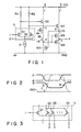
- Fig. 1 is a circuit arrangement showing an ECL-CMOS level circuit according to a first embodiment of the present invention.
- a differential-pair of transistors Q1, Q2 are provided in which an input signal is supplied from an input terminal 1 to the base of the transistor Q1 and a reference potential is supplied from an input terminal 2 to the base of the transistor Q2.
- the collectors of the transistors Q1 and Q2 are connected respectively through resistors R1 and R2 to a power source VCC and the emitters of these transistors are connected to each other via a constant current source 3.
- the collector of the transistor Q1 is connected to the base of an emitter follower transistor Q3 and the collector of the transistor Q2 is connected to the base of an emitter follower transistor Q4.
- the transistors Q1 and Q2 in that differential pair deliver their output signals to the emitter follower transistors Q3 and Q4, driving these transistors Q3 and Q4.
- the transistor Q3 has its collector connected to the power source VCC and its emitter connected to the source of a grounded-gate, P channel MOS transistor M1.
- the drain of the P channel MOS transistor M1 is connected to that of an N channel MOS transistor M2.
- the MOS transistor M2 has a grounded source and a gate connected to the emitter of the transistor Q4.
- the transistor Q4 has its collector connected to the power source VCC and its emitter connected to the source of a P channel MOS transistor M3.
- the drain the transistor M3 is connected to that of an N channel transistor M4.
- the MOS transistors M3 and M4 constitute an inverter circuit.
- the gates of the transistors M3 and M4 are commonly connected to a connection point between the transistors M3 and M4.
- the drain of the transistors M3 and M4 are connected to a common connecticn point which is connected to an output terminal 4.
- the operation of the level shift circuit will be explained below with reference to voltage waveforms at predetermined circuit points.
- the voltage waveforms show voltage levels of the respective transistors at measuring points c to f shown in Fig. 1.
- the transistors Q3 and Q4 are turned ON and OFF, respectively, when they receive corresponding differential input signals switchingly supplied from the transistors Q3 and Q4.
- a current Ia flows along a line a as shown in Fig. 1.
- a "H" level signal appears on a measuring point c on the line a and the transistor M1 is turned ON to allow a "H" level signal to emerge on the measuring point e.
- the transistor Q4 is turned OFF, the transistors M3 and M4 are turned ON upon receipt of the "H" level signal on the measuring point c so that a "L” level output appears from the CMOS inverter at the measuring point f.
- the level shift circuit is of such a type as to achieve a high-speed switching operation using a standby current.
- a "L" level voltage is used as a standby level instead of a "H” level one, whereby a drain current is reduced and hence a current Ia on the connection line a is reduced.
- a "H" level voltage emerges on the measuring point d and the transistor M2 is turned ON so that a voltage on the measuring point e goes toward a ground level. Put it in another way, a rise voltage Vth on the transistor M4 drops by an extent corresponding to a drain/ground voltage on the transistor M2 and the output of the CMOS inverter at the measuring point f goes high.
- a plurality of transistors Q1, Q2, Q3 ... Qn can be constructed, instead of the differential pair of transistors Q1, Q2 as enclosed by a broken line in Fig. 1, to supply corresponding input signals to associated circuits.
- the inverter circuit is added to the output circuit section, achieving a decreased transmission delay time and hence a high-speed processing.
- the output current capability of the output transistor can be improved with the use of the saved dissipation power, that is, the output current capabilities is improved by utilizing a saved dissipation power for an output transistor now possible to increase in size for a reason as set out above.
- the level shift circuit of the present invention can achieve a decreased transmission delay time and hence a high-speed processing and achieve an improved output current capability and hence a reduced dissipation power.
Landscapes
- Engineering & Computer Science (AREA)
- Computer Hardware Design (AREA)
- Physics & Mathematics (AREA)
- Computing Systems (AREA)
- General Engineering & Computer Science (AREA)
- Mathematical Physics (AREA)
- Logic Circuits (AREA)
- Metal-Oxide And Bipolar Metal-Oxide Semiconductor Integrated Circuits (AREA)
Applications Claiming Priority (2)
| Application Number | Priority Date | Filing Date | Title |
|---|---|---|---|
| JP1237456A JPH082019B2 (ja) | 1989-09-13 | 1989-09-13 | レベル変換回路 |
| JP237456/89 | 1989-09-13 |
Publications (3)
| Publication Number | Publication Date |
|---|---|
| EP0417786A2 true EP0417786A2 (fr) | 1991-03-20 |
| EP0417786A3 EP0417786A3 (en) | 1991-05-02 |
| EP0417786B1 EP0417786B1 (fr) | 1994-11-09 |
Family
ID=17015613
Family Applications (1)
| Application Number | Title | Priority Date | Filing Date |
|---|---|---|---|
| EP90117658A Expired - Lifetime EP0417786B1 (fr) | 1989-09-13 | 1990-09-13 | Circuit de translation de niveaux à vitesse de traitement élevée et possibilité de courant de sortie améliorée |
Country Status (5)
| Country | Link |
|---|---|
| US (1) | US5075579A (fr) |
| EP (1) | EP0417786B1 (fr) |
| JP (1) | JPH082019B2 (fr) |
| KR (1) | KR930004351B1 (fr) |
| DE (1) | DE69014035T2 (fr) |
Cited By (6)
| Publication number | Priority date | Publication date | Assignee | Title |
|---|---|---|---|---|
| EP0547333A1 (fr) * | 1991-10-25 | 1993-06-23 | Nec Corporation | Circuits semi-conducteurs |
| EP0625825A1 (fr) * | 1993-05-21 | 1994-11-23 | Nec Corporation | Circuit BI-CMOS à faible consommation de puissance, formé d'un petit nombre de composants |
| EP0627819A1 (fr) * | 1993-04-23 | 1994-12-07 | Nec Corporation | Circuit de conversion de niveau pour signaux de niveau ECL |
| DE4409453A1 (de) * | 1994-03-18 | 1995-09-21 | Thomson Brandt Gmbh | BiCMOS-Pegelwandler ECL-CMOS |
| DE19601630C1 (de) * | 1996-01-18 | 1997-06-26 | Telefunken Microelectron | Schaltungsanordnung zur Pegelumsetzung |
| US12094558B2 (en) | 2021-08-30 | 2024-09-17 | Taiwan Semiconductor Manufacturing Company, Ltd. | Multiple stack high voltage circuit for memory |
Families Citing this family (7)
| Publication number | Priority date | Publication date | Assignee | Title |
|---|---|---|---|---|
| DE4000665A1 (de) * | 1990-01-11 | 1991-07-18 | Siemens Ag | Integrierbare transistorschaltstufe der logik-familie ntl |
| JP2855802B2 (ja) * | 1990-06-27 | 1999-02-10 | 日本電気株式会社 | レベル変換回路 |
| US5254887A (en) * | 1991-06-27 | 1993-10-19 | Nec Corporation | ECL to BiCMIS level converter |
| US5485106A (en) * | 1994-04-05 | 1996-01-16 | Sun Microsystems, Inc. | ECL to CMOS converter |
| JP3123463B2 (ja) * | 1997-05-16 | 2001-01-09 | 日本電気株式会社 | レベル変換回路 |
| JP6398411B2 (ja) * | 2014-07-17 | 2018-10-03 | 富士電機株式会社 | 半導体装置および電力変換装置 |
| JP6498649B2 (ja) * | 2016-10-17 | 2019-04-10 | 株式会社東海理化電機製作所 | レベルシフタ |
Citations (3)
| Publication number | Priority date | Publication date | Assignee | Title |
|---|---|---|---|---|
| EP0146910A2 (fr) * | 1983-12-20 | 1985-07-03 | Hitachi, Ltd. | Circuit de conversion de niveau |
| EP0219867A2 (fr) * | 1985-10-23 | 1987-04-29 | Nec Corporation | Circuit logique |
| US4697109A (en) * | 1984-07-05 | 1987-09-29 | Hitachi, Ltd. | Level converter circuit |
Family Cites Families (4)
| Publication number | Priority date | Publication date | Assignee | Title |
|---|---|---|---|---|
| US4379267A (en) * | 1980-06-25 | 1983-04-05 | Mostek Corporation | Low power differential amplifier |
| JPS5943631A (ja) * | 1982-09-06 | 1984-03-10 | Hitachi Ltd | レベル変換入力回路 |
| JPS6468019A (en) * | 1987-09-08 | 1989-03-14 | Hitachi Ltd | Level converting circuit |
| JPS6474823A (en) * | 1987-09-17 | 1989-03-20 | Fujitsu Ltd | Emitter follower circuit |
-
1989
- 1989-09-13 JP JP1237456A patent/JPH082019B2/ja not_active Expired - Fee Related
-
1990
- 1990-09-11 US US07/580,559 patent/US5075579A/en not_active Expired - Lifetime
- 1990-09-12 KR KR1019900014336A patent/KR930004351B1/ko not_active IP Right Cessation
- 1990-09-13 EP EP90117658A patent/EP0417786B1/fr not_active Expired - Lifetime
- 1990-09-13 DE DE69014035T patent/DE69014035T2/de not_active Expired - Fee Related
Patent Citations (3)
| Publication number | Priority date | Publication date | Assignee | Title |
|---|---|---|---|---|
| EP0146910A2 (fr) * | 1983-12-20 | 1985-07-03 | Hitachi, Ltd. | Circuit de conversion de niveau |
| US4697109A (en) * | 1984-07-05 | 1987-09-29 | Hitachi, Ltd. | Level converter circuit |
| EP0219867A2 (fr) * | 1985-10-23 | 1987-04-29 | Nec Corporation | Circuit logique |
Non-Patent Citations (1)
| Title |
|---|
| IEEE JOURNAL OF SOLID-STATE CIRCUITS vol. 23, no. 5, October 1988, pages 1036,1037; YANG et al.: "4-NS 4K X 1-Bit two-port Bicmos sram" * |
Cited By (10)
| Publication number | Priority date | Publication date | Assignee | Title |
|---|---|---|---|---|
| EP0547333A1 (fr) * | 1991-10-25 | 1993-06-23 | Nec Corporation | Circuits semi-conducteurs |
| US5382845A (en) * | 1991-10-25 | 1995-01-17 | Nec Corporation | ECL to CMOS level converter |
| EP0627819A1 (fr) * | 1993-04-23 | 1994-12-07 | Nec Corporation | Circuit de conversion de niveau pour signaux de niveau ECL |
| US5465057A (en) * | 1993-04-23 | 1995-11-07 | Nec Corporation | Level conversion circuit for signal of ECL-level |
| EP0625825A1 (fr) * | 1993-05-21 | 1994-11-23 | Nec Corporation | Circuit BI-CMOS à faible consommation de puissance, formé d'un petit nombre de composants |
| US5479005A (en) * | 1993-05-21 | 1995-12-26 | Nec Corporation | Low-power consumption bi-CMOS circuit formed by a small number of circuit components |
| DE4409453A1 (de) * | 1994-03-18 | 1995-09-21 | Thomson Brandt Gmbh | BiCMOS-Pegelwandler ECL-CMOS |
| US5631580A (en) * | 1994-03-18 | 1997-05-20 | Deutsche Thomson-Brandt Gmbh | BICMOS ECL-CMOS level converter |
| DE19601630C1 (de) * | 1996-01-18 | 1997-06-26 | Telefunken Microelectron | Schaltungsanordnung zur Pegelumsetzung |
| US12094558B2 (en) | 2021-08-30 | 2024-09-17 | Taiwan Semiconductor Manufacturing Company, Ltd. | Multiple stack high voltage circuit for memory |
Also Published As
| Publication number | Publication date |
|---|---|
| DE69014035D1 (de) | 1994-12-15 |
| EP0417786A3 (en) | 1991-05-02 |
| JPH082019B2 (ja) | 1996-01-10 |
| EP0417786B1 (fr) | 1994-11-09 |
| KR910007277A (ko) | 1991-04-30 |
| US5075579A (en) | 1991-12-24 |
| KR930004351B1 (ko) | 1993-05-26 |
| JPH0399516A (ja) | 1991-04-24 |
| DE69014035T2 (de) | 1995-04-27 |
Similar Documents
| Publication | Publication Date | Title |
|---|---|---|
| US4890017A (en) | CMOS-BiCMOS gate circuit | |
| KR0136775B1 (ko) | 스위칭 유도 잡음을 감소시키는 출력 버퍼 | |
| KR900008051B1 (ko) | 논리회로 | |
| US4804869A (en) | BiMOS logical circuit | |
| EP0417786A2 (fr) | Circuit de translation de niveaux à vitesse de traitement élevée et possibilité de courant de sortie améliorée | |
| US4725982A (en) | Tri-state buffer circuit | |
| US5214317A (en) | CMOS to ECL translator with incorporated latch | |
| US5663659A (en) | Semiconductor integrated circuit device comprising CMOS transistors and differentiator | |
| JPH0583004B2 (fr) | ||
| KR930001439B1 (ko) | BiCMOS용 출력회로 | |
| EP0473409B1 (fr) | Circuit logique BiCMOS | |
| US4977338A (en) | High speed bipolar-MOS logic circuit including a series coupled arrangement of a bipolar transistor and a logic block having a MOSFET | |
| US4977337A (en) | Bi-CMOS logic circuit | |
| EP0452919A2 (fr) | Circuit intégré semi-conducteur Bi-MOS | |
| US5107143A (en) | Signal output circuit included in bus driving integrated circuit | |
| US4900954A (en) | Mixed CML/ECL macro circuitry | |
| US5057714A (en) | BiCMOS integrated circuit device utilizing Schottky diodes | |
| EP0432472A2 (fr) | Circuit CMOS comportant des transistors bipolaires dans l'étage de sortie | |
| US5239212A (en) | Gate circuit of combined field-effect and bipolar transistors with an improved discharge arrangement | |
| KR950000352B1 (ko) | 반도체 논리회로 | |
| EP0439894A1 (fr) | Circuit logique à semi-conducteur | |
| KR100350820B1 (ko) | 넓은전원범위에서동작하기에적합한 저전압BiCMOS디지털지연체인 | |
| KR900008050B1 (ko) | 논리회로 | |
| US5600268A (en) | Gate circuit of combined field-effect and bipolar transistors | |
| JP2929869B2 (ja) | 3ステート・バッファ回路 |
Legal Events
| Date | Code | Title | Description |
|---|---|---|---|
| PUAI | Public reference made under article 153(3) epc to a published international application that has entered the european phase |
Free format text: ORIGINAL CODE: 0009012 |
|
| PUAL | Search report despatched |
Free format text: ORIGINAL CODE: 0009013 |
|
| 17P | Request for examination filed |
Effective date: 19900913 |
|
| AK | Designated contracting states |
Kind code of ref document: A2 Designated state(s): DE FR GB |
|
| AK | Designated contracting states |
Kind code of ref document: A3 Designated state(s): DE FR GB |
|
| 17Q | First examination report despatched |
Effective date: 19930804 |
|
| GRAA | (expected) grant |
Free format text: ORIGINAL CODE: 0009210 |
|
| AK | Designated contracting states |
Kind code of ref document: B1 Designated state(s): DE FR GB |
|
| REF | Corresponds to: |
Ref document number: 69014035 Country of ref document: DE Date of ref document: 19941215 |
|
| ET | Fr: translation filed | ||
| PLBE | No opposition filed within time limit |
Free format text: ORIGINAL CODE: 0009261 |
|
| STAA | Information on the status of an ep patent application or granted ep patent |
Free format text: STATUS: NO OPPOSITION FILED WITHIN TIME LIMIT |
|
| 26N | No opposition filed | ||
| PGFP | Annual fee paid to national office [announced via postgrant information from national office to epo] |
Ref country code: GB Payment date: 19970904 Year of fee payment: 8 |
|
| PGFP | Annual fee paid to national office [announced via postgrant information from national office to epo] |
Ref country code: FR Payment date: 19970909 Year of fee payment: 8 |
|
| PG25 | Lapsed in a contracting state [announced via postgrant information from national office to epo] |
Ref country code: GB Free format text: LAPSE BECAUSE OF NON-PAYMENT OF DUE FEES Effective date: 19980913 |
|
| GBPC | Gb: european patent ceased through non-payment of renewal fee |
Effective date: 19980913 |
|
| PG25 | Lapsed in a contracting state [announced via postgrant information from national office to epo] |
Ref country code: FR Free format text: LAPSE BECAUSE OF NON-PAYMENT OF DUE FEES Effective date: 19990531 |
|
| REG | Reference to a national code |
Ref country code: FR Ref legal event code: ST |
|
| PGFP | Annual fee paid to national office [announced via postgrant information from national office to epo] |
Ref country code: DE Payment date: 20050909 Year of fee payment: 16 |
|
| PG25 | Lapsed in a contracting state [announced via postgrant information from national office to epo] |
Ref country code: DE Free format text: LAPSE BECAUSE OF NON-PAYMENT OF DUE FEES Effective date: 20070403 |