EP0417707A2 - Mikrorechner mit Adressenregistern für dynamische Bussteuerung - Google Patents
Mikrorechner mit Adressenregistern für dynamische Bussteuerung Download PDFInfo
- Publication number
- EP0417707A2 EP0417707A2 EP90117417A EP90117417A EP0417707A2 EP 0417707 A2 EP0417707 A2 EP 0417707A2 EP 90117417 A EP90117417 A EP 90117417A EP 90117417 A EP90117417 A EP 90117417A EP 0417707 A2 EP0417707 A2 EP 0417707A2
- Authority
- EP
- European Patent Office
- Prior art keywords
- address
- data
- bus
- bit
- microcomputer
- Prior art date
- Legal status (The legal status is an assumption and is not a legal conclusion. Google has not performed a legal analysis and makes no representation as to the accuracy of the status listed.)
- Withdrawn
Links
Images


Classifications
-
- G—PHYSICS
- G06—COMPUTING OR CALCULATING; COUNTING
- G06F—ELECTRIC DIGITAL DATA PROCESSING
- G06F13/00—Interconnection of, or transfer of information or other signals between, memories, input/output devices or central processing units
- G06F13/14—Handling requests for interconnection or transfer
- G06F13/36—Handling requests for interconnection or transfer for access to common bus or bus system
-
- G—PHYSICS
- G06—COMPUTING OR CALCULATING; COUNTING
- G06F—ELECTRIC DIGITAL DATA PROCESSING
- G06F13/00—Interconnection of, or transfer of information or other signals between, memories, input/output devices or central processing units
- G06F13/38—Information transfer, e.g. on bus
- G06F13/40—Bus structure
- G06F13/4004—Coupling between buses
- G06F13/4009—Coupling between buses with data restructuring
- G06F13/4018—Coupling between buses with data restructuring with data-width conversion
Definitions
- the present invention relates generally to a microcomputer and, more particularly, to a single chip microcomputer capable of constituting a data processing system together with a system resource having different data bus sizes or cycles.
- the internal memory to be programmed is made of an electrically programmable read only memory (as will be referred to as "EPROM");
- EPROM electrically programmable read only memory
- the number of bits or the general-purpose registers themselves to be packaged in the microcom puter is increased; and the internal peripheral circuits of the microprocessor are exemplified, considering various applications, by a free running timer, an analog-to-digital converter, a pulse width modulation (i.e,. PWM) timer, a serial communication interface circuit or a direct memory access controller.
- PWM pulse width modulation
- a wait control circuit is packaged in a microprocessor so as to facilitate the interface with a low speed memory such as a dynamic random access memory, or a dynamic bus sizing function is given to the microprocessor.
- the dynamic bus sizing function is one to give the microcomputer dynamically a 4-bit interface or an 8-bit interface so as to make possible the data exchange between an external device having a data bus width of 4 or 8 bits and an external microcomputer of 16-bit interface in case the width of the data bus belonging intrinsically to the microcomputer, i.e,. the number of external data terminals is 16 bits, for example.
- the function to change the bus operations dynamically according to the various external conditions is called the dynamic bus sizing function.
- This dynamic bus sizing function is important for dropping the cost of a data processor system having the microcomputer and for augmenting the degree of freedom for designing the aforementioned data processor system.
- the present invention has been conceived in the course of enhancing the general-purpose properties of the aforementioned dynamic bus sizing function and pursuing the high-speed operations.
- An object of the present invention is to provide a microcomputer enabled to change the bus size dynamically at a high speed and with general-purpose properties and a method for the microcomputer.
- Another object of the present invention is to provide a microcomputer enabled to change not only the bus sizes but also the bus cycles dynamically and a method for the microcomputer.
- a microcomputer there are packaged one or more registers, by which a specific address area can be accessed.
- the microprocessor itself acknowledges the access, if any to the address in the specific address area, to change the data bus width of the microcomputer dynamically.
- the microprocessor itself acknowledges whether or not the address to be accessed is the specific address area set in the aforementioned registers, and can change the bus width dynamically at a high speed and with the general-purpose properties.
- the bus controller of the microcomputer comprises: a first address register for addressing an address area (or range) for which a bus width is to be changed; a second address register for addressing an address area (or range) for which a bus cycle is to be changed; and comparison means for comparing the individual address areas addressed by said first and second address registers and an address signal out-putted from a bus master such as a central processing unit onto an internal address bus.
- the degree of freedom for selecting a memory unit or a peripheral circuit to be incorporated into the aforementioned data processing system so that the degree of freedom for designing the system can be drastically improved. Thanks to this improvement in the degree of freedom for the selection, moreover, a memory unit or a peripheral circuit at a low cost can be selected to drop the cost for the data processing system.
- Fig. 1 shows a data processing system according to the present invention.
- a microcomputer 1 is formed in one semiconductor substrate of single-crystalline silicon or the like, as designated by single-dotted lines, by the well-known technology for forming the CMOS.
- the microcomputer 1 is equipped with twenty four address output terminals A0 to A23 and sixteen input/output terminals D0 to D15, through which it is linked to an external address bus (SAB) 2 including twenty four signal lines and an external data bus (SDB) 3 including sixteen signal lines.
- SAB external address bus
- SDB external data bus
- the microcomputer 1 is designed on the basis of such a 16-bit architecture that the input/output bit number of data to the outside can be executed at a unit of 16 bits (i.e., 1 word).
- the external data bus 3 is composed of an 8-bit external data bus SDB(H) of higher rank and an 8-bit external data bus SDB(L) of lower rank.
- san external random access memory (RAM) 6, an external read only memory (ROM) 7 and a direct memory access controller (DMAC) 8 which are designed on the basis of the 16-bit architecture, are linked to the microcomputer 1 through the aforementioned external address bus 2 and external data bus 3.
- the system resources (PIA4 and FDC5) having a data bus size different from the data bus size (i.e., 16 bits) of the microcomputer 1 are packaged in the data processing system.
- this microcomputer 1 includes a later-described bus controller (BUS CONT) 40 into which the dynamic data bus sizing function is incorporated.
- a microprocessor unit MPU 10 includes: an execution unit having a variety of 16-bit registers such as a 16-bit arithmetic logic unit (ALU) or a program counter; and a sequence control unit for controlling the operations of the execution unit.
- the sequence control unit includes: a macro instruction register for holding a macro instruction; a macro instruction decoder for decoding the output of the macro instruction register; a micro ROM adapted to be controlled by the outputs of the macro instruction decoder and having a plurality of micro instructions; and a micro instruction decoder for decoding the micro instructions outputted from the micro ROM to control the operations of the aforementioned execution unit substantially.
- the micro ROM is accessed at first by the outputs of the macro instruction decoder. Then, the micro ROM is accessed on the basis of the next address data in a next address field of the micro instructions outputted from the micro ROM. In other words, in order to execute one macro instruction, one or plural micro instructions are sequentially read out from the micro ROM.
- the aforementioned microcomputer 1 further comprises internal modules: a 16-bit output read only memory (ROM) 12 for storing a data processing program; a 16-bit input/output random access memory (RAM) for providing operation areas for the aforementioned CPU 10 and storing data; an analog-to-digital converter (A/D CONV) 16 for converting analog signals to digital data; a serial communication interface circuit (SCI) 18 for converting either serial data inputted from the outside of the microcomputer 1 to parallel data or internal data of the microcomputer 1 to serial data to output them to the outside of the microcomputer 1; a timer (TM) 20; and a free running timer (FRT) 22.
- ROM read only memory
- RAM input/output random access memory
- A/D CONV analog-to-digital converter
- SCI serial communication interface circuit
- TM timer
- FRT free running timer
- the aforementioned A/D converter 16 receives input signals from analog sensors 23 such as temperature sensors, which are disposed outside of the microcomputer 1, through external terminals AN0 and AN1 to convert the analog signal inputted to the external terminal AN0 or AN1 to a digital signal in accordance with a program.
- the A/D converter 16 includes therein a 8-bit data register for storing the converted digital data and a control register for controlling the operations of the A/D converter 16.
- This control register is made to have a storage capacity of 8 bits, for example, and a predetermined address and can be read and written by the MPU 10.
- the aforementioned data register has a predetermined address so that the data stored therein are read out by the access of the MPU 10.
- serial communication interface (SCI) 18 is linked to a peripheral device 27 through a serial clock input/output terminal SCK, a serial data input terminal RXD and a serial data output terminal TXD.
- serial communication interface (SCI) 18 is in a clock synchronization mode, for example, it outputs serial data (or transfer data) to the aforementioned terminal TXD in synchronism with the aforementioned transfer clock while outputting the transfer clock through the aforementioned terminal SCK.
- the aforementioned SCI 18 receives the reception clock inputted at the aforementioned terminal SCK and the serial data (or reception data) synchronized with the reception clock through the terminal RXD.
- the SCI 18 is exemplified by including a readable 8-bit reception data register, a readable/writable 8-bit transmission data register and a readable/writable 8-bit control register, all of which are adapted to be accessed by the MPU.
- the aforementioned timer (TM) 20 is linked to the peripheral device 27 through a timer output terminal TMO, a timer clock input terminal TMCI and a timer reset input terminal TMRI.
- the timer (TM) 20 includes therein a 8-bit counter and a 8-bit readable/writable time constant register.
- the counter counts either at the rise or break or at the edge of the rise/break of an external clock inputted to the terminal TMCI.
- the counted value of the counter is compared with the time constant data which is set in the time constant register by the MPU 10. In case the comparison finds out a coincidence, the timer (TM) 20 outputs a coincidence signal (or a compare match signal) to the terminal TMO.
- the counted value of the counter can be reset, if necessary, with a clear signal to be applied to the aforementioned terminal TMRI
- the timer (TM) 20 includes a readable/writable 8-bit control register to be accessed by the MPU so as to control the operations of the timer (TM) 20.
- the aforementioned free running timer (FRT) 22 is linked to the peripheral device 27 through output compare signal output terminals FTOA and FTOB and an input capture signal input terminal FTI.
- the timer FRT 22 includes a 16-bit free running counter, readable/writable 16-bit first and second output compare registers, a readable 16-bit input capture register, a readable/writable 8-bit timer control register, and a readable/writable 8-bit timer status register.
- the 16-bit register is adapted to be read or written for every 8 bits by the MPU 10.
- both the upper limit value (e.g., "A000" in the hexadecimal notation) of the counted value of the free running counter and the half value (e.g. , "5000" in the hexadecimal) of the upper limit data of the free running counter are written in the first and second output compare registers, respectively, by the MPU 10. Moreover, the counter clear bit of the timer status register is set, and the free running counter is reset with the value ("A000") set in the first output compare register.
- the pulse signal outputted from the terminal FTOA is made so periodic that it is given a high level for a time period from a reset to a subsequent reset of the free running counter and a low level for a time period from the subsequent reset to a further subsequent reset.
- the pulse signal to be outputted from the terminal FTOB has its output level inverted each time the value ("5000") of the second output compare register and the counted value of the free running counter match each other.
- the two pulse signals to be outputted from the terminals FTOA and FTOB have a duty ratio of 50 % and an out-of phase of 90 degrees.
- the counted value of the free running counter is set in the input capture register.
- the MPU 10 is enabled to measure the period or width of the pulses by reading out the counted value which is set in the input capture register.
- each of the peripheral circuits e.g., A/D CONV, SCI, TM and FRT
- the register which can be accessed by the MPU 10.
- Predetermined different addresses are assigned to those individual registers. Predetermined addresses are naturally assigned to the storage areas in the internal ROM 12 and RAM 14 and the various registers in the MPU 10. As a result, the predetermined individual addresses are assigned to the address spaces of the MPU 10.
- the microcomputer 1 has the following components.
- a clock pulse generator MPG generates a variety of clock pulses for controlling the operation timing of the MPU 10 and the operations of the internal peripheral modules (e.g., A/D CONV 16, SCI 18, TM 20 and FRT 22).
- the CPG 24 is connected with the quarts oscillator 26, for example, through external terminals X1 and X2 and generates a system clock ⁇ of 10 MHz, for example, by halving the frequency of the original frequency (e.g., 20 MHz) generated from the quarts oscillator 26.
- the CPG 24 further generates clock pulses ( ⁇ /2 to ⁇ /4096) for the peripheral modules 16, 18, 20 and 22.
- An interrupt controller (INT CONT) 28 receives both interrupt requests, which are inputted from the PIA4 and the DMAC 16 through external terminals INTO and INTI, and an internal interrupt request IINT, which is inputted from the peripheral modules 16, 18, 20 and 22, to generate an interrupt request INT to the MPU 10.
- the INT CONT 28 includes a readable/writable 8-bit priority control register and responds to one of a higher rank of plural interrupt requests, if any, in accordance with a predetermined priority.
- the MPU 10 is shifted from an ordinary data processing mode (i.e., an operation mode according to the program in the ROM 12) to an interrupt processing routine to execute the interruption to the interrupt request.
- a mode controller (MODE CONT) 30 is linked through external terminals MD0, MD1 and MD2 to a mode setting circuit (MODE SET CKT) 32 and acknowledges the voltage level (e.g., a high or low level) of the terminals MD0 to MD2 set by the mode setting circuit 32 to generate a mode signal MD for the MPU 10 and the later-described bus controller 40.
- the mode controller 30 can acknowledge a combination of eight kinds of voltage levels of the individual terminals MD0, MD1 and MD2.
- the microcomputer 1 has five kinds of operation modes, i.e, a single chip mode, extended minimum modes 1 and 2, and extended maximum modes 3 and 4, all of which are acknowledged by the aforementioned mode controller 30.
- the mode signal MD is deemed to contain five signals in correspondence to the five kinds of modes.
- Fig. 1(b) is a memory map of an address space enumerating the aforementioned five kinds of modes.
- letter R designates address areas of the aforementioned or later-described various registers in the internal blocks 16, 18, 20, 22, 28, 36 and 40; letters IRAM designate address areas of the RAM 14; letters IROM designate address areas of the ROM 12; letters EX designate address areas of the external memories (RAM 6 and ROM 7) and various registers in the external peripheral circuits (PIA 4, FDC5 and DMAC 8) which can be accessed by the microcomputer 1; and letter B designates vector access for interrupt and exceptional processings.
- Fig. 1(b) In case the microcomputer 1 is not equipped with the ROM 12 and RAM 14, its operation modes are the aforementioned modes 1, 2, 3 and 4, and the IRAM and IROM in Fig. 1(b) are address areas EX. In Fig. 1(b), moreover, the first and last addresses of the address areas are expressed in the hexadecimal notation.
- the microcomputer 1 shown in Fig. 1(a) further includes the following components.
- a system controller (SYS CONT) is linked to the DMAC 8 through external terminals X3 and X4 and to the MPU 10.
- This SYS CONT 34 controls whether or not a bus acknowledgment BACK is to be generated to the DMAC 8, when the DMAC generates a bus request BREQ in response to a data transfer request TRQ from the FDC 5.
- the DMAC issues a data transfer acknowledgment TAC to the FDC 5, when it receives the bus acknowledgment, to execute the direct memory access.
- the SYS CONT 34 has a bus arbiter function.
- a wait state controller (WAIT CONT) 36 is linked through an external terminal WAIT to the low-speed external device (FDC5 or ROM 7).
- the WAIT CONT 36 includes an 8-bit control register which can be read and written by the MPU 10.
- the WAIT CONT 36 is provided for facilitating the interface between the aforementioned low-speed external device and the microcomputer 1 and outputs a wait signal WT to the MPU 10 so as to elongate the bus cycle by inserting a predetermined number of wait states into the bus cycle.
- the aforementioned register is provided for selecting the wait modes and the wait state number.
- the wait modes are: a programmable wait mode in which wait states of a number selected when the MPU 10 accesses the external address space are inserted into the bus cycle; a terminal wait mode in which wait states of a number selected when the MPU 1 accesses the external address space are inserted into the bus cycle and in which the wait states are continuously inserted till the aforementioned terminal WAIT is raised to the high level in case the terminal WAIT is at the low level; and an auto-wait mode in which wait states of a number selected only when the terminal WAIT is at the low level are inserted into the bus cycle.
- a programmable wait mode in which wait states of a number selected when the MPU 10 accesses the external address space are inserted into the bus cycle
- a terminal wait mode in which wait states of a number selected when the MPU 1 accesses the external address space are inserted into the bus cycle and in which the wait states are continuously inserted till the aforementi
- An address output buffer (AOB) 38 has a function to output an address signal, which is outputted from the MPU 10 acting as the bus master and received through the internal address AB, to the external address bus SAB through the address output terminals A0 to A23.
- a data input/output buffer (IOB) 50 outputs the data on the internal data bus DB to the external data bus SDB through the data input/output terminals D0 to D15 or inputs the data on the internal data bus SDB, which are received through the data input/output terminals D0 to D15, to the internal data bus.
- the data input/output buffer 50 has its operations controlled by control signals BS, DOC and DIC which are outputted from the MPU 10.
- Terminals X5 and X6 are fed with the operation voltages Vcc at 5 volts or the like and GND at 0 volts or the like of the microcomputer 1, and terminals X7 and X8 are fed with reference voltages AVcc and AGND of the A/D CONV 16.
- the bus controller (BUS CONT) 40 is linked to the external peripheral circuits 4, 5, 6, 7 and 8 through external terminals AS , RD , HWR and LWR to generate address strobe signal, a read signal, a higher byte write signal and a lower byte write signal at the aforementioned terminals AS , RD , HWR and LWR , respectively, in response to a control signal C coming from the MPU 10 when the MPU 10 accesses the external address space.
- the bus controller 40 includes: a timing signal generator for generating the address strobe signal, the read signal, the higher byte write signal and the lower byte write signal on the basis of the aforementioned control signal C; and an address detector for changing the data bus size.
- Fig. 2 shows the detector in the bus controller which has a circuit structure, as will be described in the following.
- Registers (RA) 401 and (RB) 402 individually have a bit width of 1 bit or more and are used for addressing the address areas. These registers RA and RB are made to have a storage capacity of 8 bits, i.e,. a 8-bit structure. This structure of the register RA or RB is shown in Fig. 3.
- registers RA and RB are assigned with specific addresses like the various registers owned by the MPU 10 and are connected with the internal data bus DB. As a result, an arbitrary address area can be addressed by writing the registers RA and RB from the MPU 10.
- the address information held in the register RA is inputted to a comparator CPA 403.
- the address information held in the register RB is inputted to the comparator CPB 404.
- the comparators CPA and CPB have their other inputs fed through the internal address bus AB with the address signal to be accessed by the MPU 10.
- the comparators CPA and CPB compare the address information set in the registers RA and RB and the address signal on the internal address bus to output comparison result signals CRS1 and CRS2. These result signals are transmitted to the MPU 10 to discriminate from the comparison output result CRS of the two comparators CPA and CPB whether or not the external address to be accessed belongs to the specific address area addressed by the registers RA and RB. This discrimination result is reflected upon the control signal BS.
- the IOB 50 is interposed between the internal data bus DB and the external data bus (or system bus) SDB. This IOB 50 performs a bus width change, as will be described hereinafter, in response to the aforementioned control signal (or bus width select signal) BS.
- the aforementioned mode signal MD is fed to the comparators CPA and CPB.
- the address bus AB outputs a 16-bit address signal to the outside to enable the MPU 10 to access an area of about 64 Kbytes.
- the address bus AB outputs of a 24-bit address to enable the MPU to access an area of about 16 Mbytes.
- the corresponding comparators CPA and CPB have an input of a 8-bit width.
- the address signal of 8 bits which is inputted to the comparators CPA and CPB, is the higher 8 bits (i.e., 8th to 15th) of the address signal of 16 bits.
- the area addressing unit for the registers RA and RB to address is 256 bytes. If a common address information is inputted to the registers RA and RB, for example, it is used as the higher 8-bit address for addressing the area of 256 bytes.
- the 8-bit address signal to be inputted to the comparators CPA and CPB is the higher 8 bits (i.e., 16th to 23rd) of the address signal of 24 bits.
- the area addressing unit for the registers RA and RB to address is about 64 Kbytes. If a common address information is inputted to the registers RA and RB, for example, it is used as the higher 8-bit address for addressing the area of about 64 Kbytes.
- the bit structure of the registers RA and RB should not be limited to that shown in Fig. 3 but may be made to have 24 bits, respectively. According to the structure of Fig. 3, however, the cost for the microcomputer 1 can be dropped.
- Fig. 4 is a conceptional diagram showing the address space to be designated by the aforementioned registers. Incidentally, the letters EX appearing in Fig. 4 are construed to indicate the letters EX in the memory map relating to the modes 1 to 4 shown in Fig. 2.
- the MPU decides whether or not the aforementioned area is designated from the comparison outputs of the aforementioned comparators CPA and CPB. If in the address designated area, the control signal BS is generated to make a change to the interface through the 8-bit bus. Otherwise, the interface is the bus interface of 16 bits.
- the advantage of the method thus far described is that the external device of 8-bit architecture can be freely adopted in the data processing system even in case the external address area is in the middle of the memory map, as in the minimum extension modes 1 and 2.
- Fig. 5 is a circuit diagram showing one embodiment of the output line of the input/output buffer IOB 50 having the aforementioned bus width changing func tion.
- a multiplexer which is constructed of a clocked inverter (i.e., a three-state output circuit), although not limited thereto.
- the signals ID0 to ID7 of the internal data bus DB are fed to the inputs of the corresponding output circuits DOB0 to DOB7 through clocked inverters CN0 to CN1.
- the higher 8-bit signals ID8 to ID15 of the internal data bus DB are fed on one hand to the inputs of DOB8 to DOB15 corresponding to the higher 8 bits of the 16-bit bus width through clocked inverters CN2 and CN3, as illustrated as representatives, and on the other hand to the inputs of the output circuits DOB0 to DOB7 corresponding to the 8-bit bus width through clocked inverters CN4 and CN5, as illustrated as representatives.
- a control signal L is fed to the control terminals of the aforementioned clocked inverters CN0 and CN1.
- a control signal U is fed to the control circuits of the aforementioned clocked inverters CN2 and CN3.
- a control signal U′ is fed to the control terminals of the clocked inverters CN4 and CN5.
- These individual clocked inverters CN0 to CN5 are rendered operative to transmit their signals, when the corresponding control signals L, U and U′ are at the high level (i.e., the logic "1"), and are brought into an output high-impedance state when the corresponding control signals L, U and U′ are at the low level (i.e., the logic "0").
- the output circuits DOB0 to DOB15 have their operations controlled with the output control signal DOC to be outputted from the MPU 10.
- the output control signal DOC is raised to the high level. Accordingly, the output circuits DOB0 to DOB15 are rendered operative to output the write data or the like generated by the MPU 10.
- the output control signal DOC is dropped to the low level. Accordingly the output circuits DOB0 to DOB15 are brought into the output high-impedance state "Z" so that the data input circuit of Fig. 6 is rendered operative to input the data from a system bus ADB.
- Fig. 6 shows one embodiment of the input line of the input/output buffer IOB 50.
- Clocked inverters CNi are disposed downstream of the input circuits DIC0 to DIC15 which are made receptive of the signals of the external data buses SDB(H) and SDB(L) at their inputs.
- the MPU In the read cycle as when these clocked inverters CNi receive the input control signals DiC at their control gates, e.g., when the clocked inverters read data from the outside, the MPU outputs the input control signal DiC at the high level to render the clocked inverters CNi conductive. Since, at this time, the MPU 10 outputs the output control signal DOC at the low level so that the outputs of the output circuits DOB0 to DOB15 are brought into the high-impedance state ("Z").
- the outputs of the aforementioned inverters CNi are linked to the internal data bus DB through both inverters INV0 to INV15 and a multiplexer including the clocked inverters CN6 to CN11.
- the clocked inverters CN6 to CN9 in the multiplexer transmit the data on the external terminals D0 to D15 as the internal data ID0 to ID15 to the internal data bus DB.
- the clocked inverters CN10 and CN11 transmit the data on the external terminals D0 to D7 as the internal data ID8 to ID15 to the higher 8 bits of the internal data bus DB.
- control signals L′ , U ⁇ and U′′′ are caused to take either the high, low and low levels or the low, high and low levels.
- Fig. 7 shows a circuit example of the clock inverters CN shown in Figs. 5 and 6, and Fig. 8 shows a circuit example of the output circuit DOB1 of Fig. 5.
- Both of these circuits are constructed of CMOS circuits containing P-ch MOSFETs and N-ch MOSFETs. The operations of these circuits will not be described because they seem well known to those skilled in the art.
- Fig. 9 is a timing chart showing the operations of the write cycle of the aforementioned input/output buffer IOB shown in Fig. 5.
- the MPU 10 outputs an address signal n corresponding to an address in the bus interface area of 16 bits, as shown in Fig. 4, to the internal address bus AB in case it is going to access said address.
- the MPU 10 acknowledges from the outputs of the comparators CPA and GPB that the address belongs to the bus width area of 16 bits.
- the MPU 10 sets, as the control signals BS, the control signals U and L to the logic "1" and the control signal U′ to the logic "0".
- the aforementioned clocked inverters CN0 and CN1, and CN2 and CN3 are rendered operative.
- the lower 8-bit signals ID0 to ID7 on the internal data bus DB are transmitted to the inputs of the output circuits DOB0 to DOB7 through the clocked inverters CN0 and CN1, as illustrated as representatives.
- the higher 8-bit signals IDB to ID15 of the internal data bus DB are transmitted to the inputs of the output circuits DOB8 to DOB15 through the clocked inverters CN2 and CN3, as illustrated as representatives.
- the 16-bit data composed of the ID0 to ID7 and ID8 to ID15 are transmitted in one write cycle containing first and second states T1 and T2 to external data buses SDB(H) and SDB(L) of 16-bit width through the output terminals D0 to D15.
- both the higher byte write signal HWR and the lower byte write signal LWR are dropped in the second state T2 to the low level to inform the external device such as a memory of the fact that the write cycle has the 16-bit data.
- the MPU 10 In case, on the other hand, the MPU 10 is going to access the address in the bus interface area of 8 bits, as shown in Fig. 4, it outputs the address signal n corresponding to the aforementioned to the internal address bus AB. From the outputs of the comparators CPA and CPB, the MPU 10 acknowledges that the address belongs to the bus width area of 8 bits. As a result, the MPU 10 sets, as the control signals BS, the signal L to the logic "1" and the signals U and U′ to the logic "0" in the first one write cycle. As a result, only the aforementioned clocked inverters CN0 and CN1 are rendered operative.
- the lower 8-bit signals ID0 to ID7 of the internal data bus DB are transmitted to the inputs of the output circuits DOB0 to DOB7 through the clocked inverters CN0 and CN1, as illustrated as representatives.
- the data composed of 8 bits ID0 to ID7 are transmitted through the output terminals D0 to D7 to the external data bus SDB(H) of the lower 8 bits of the external data bus SDB having the 16-bit width.
- the lower byte write signal LWR is set to the low level in the second state T2 and informs the external device such as FDCS of the fact that the write cycle has the lower 8-bit data.
- the output terminals D8 to D15 corresponding to the external data bus SDB(L) of the higher 8 bits of the external data bus SDB are in the high impedance ("Z"), as shown, in response to the high impedance of the outputs of the aforementioned clocked inverters CN2 to CN5.
- Z high impedance
- the control terminals of the clocked inverters CN0 to CN3 may be shared and fed with the control signal L.
- the MPU 10 increments the address signal n on the internal address bus AB on the basis of the logic "0" of the signal U and sets the signal U′ to the logic "1" and the signals L and U to the logic "0".
- the MPU 10 increments the address signal n on the internal address bus AB on the basis of the logic "0" of the signal U and sets the signal U′ to the logic "1” and the signals L and U to the logic "0".
- the aforementioned clocked inverters CN4 and CN5 are rendered operative.
- the higher 8-bit signals ID8 to ID15 of the internal data bus DB are transmitted to the inputs of the output circuits DOB0 to DOB7 through the clocked inverters CN4 and CN5, as illustrated as representatives.
- the data of the remaining 8 bits IDB to ID15 are transmitted during one write cycle through the output terminals D0 to D7 to the external data bus SDB(L) of the lower 8 bits of the external data bus SDB of the 16-bit width.
- the lower byte write signal LWR is set to the low level in the second state T2 and informs the peripheral device such as FDC5 of the fact that the write cycle has the lower 8-bit data.
- the data ID0 to ID15 of 16 bits outputted from the MPU 10 are written in the peripheral device during the two write cycles by the but interface of 8 bits.
- Fig. 10 is a timing chart showing the operations of the read cycle of the aforementioned input/output buffer IOB shown in Fig. 6.
- the MPU 10 reads the data of 16 bits from the address n in the bus interface area of 16 bits shown in Fig. 4, it sets, as the control signals BS, the logic signals L′ and U′′′ to the logic "1" and the logic signal U ⁇ to the logic "0" on the basis of the outputs of comparators CPA and CPB.
- the aforementioned clocked inverters CN6 and CN7, and CN8 and CN9 of Fig. 6 are rendered operative.
- the 16-bit data on the external data bus SDB are transmitted through the external terminals D0 to D15 to the internal data buses DB(H) and DB(L).
- the 16-bit data are to be read by the MPU 10 from the 8-bit bus interface area shown in Fig. 4, the following operations are executed.
- the MPU 10 transmits the address signal n onto the internal address bus AB.
- the MPU 10 sets, as the control signals BS, the control signal L7 to the logic "1" and the logic signals U ⁇ and U′′′ to the logic "0".
- the aforementioned clocked inverters CN6 and CN7 of Fig. 6 are rendered operative.
- the 8-bit data of the lower external data bus SBD(L) are transmitted through the external terminals D0 to D7 to the lower internal data bus DB(L).
- the MPU 10 increments the address signal n on the internal address AB on the basis of the logic "0" of the signal U′′′ of the preceding cycle and sets the control signal U ⁇ to the logic "1" and the control signals U′′′ and L′ to the logic "0".
- the clocked inverters CN10 and CN11 of Fig. 6 are rendered operative.
- the 8-bit data on the external data bus SDB(L) are transmitted through the external terminals D0 to D7 to the higher internal data bus DB(H).
- the present embodiment Since, according to the present embodiment, an arbitrary address information can be written in the registers RA and RB, the degree of freedom for the user to address the area is increased. Since, moreover, the present embodiment is effective for all the bus cycles, there is no restriction upon the specific instruction or the operation of the data transfer. Since, furthermore, the signals are decoded in the microprocessor, a gate delay time from the output of the address signal to the control signals BS is about 10 to 20 nsecs at the maximum, the high-speed access can be attained without any restriction upon the speed unlike the case in which the signals are to be decoded outside of the chip.
- a control circuit for determining whether the 8-bit bus interface or the 16-bit bus interface is outside of the chip: it takes 30 nsecs for the address signal to be transmitted to the external address but; it takes 10 nsecs to decode and compare the address signals; and it takes a setup time of 10 to 20 nsecs to input a signal such as the control signals BS to the external device. In short, a time of 50 nsecs or more is required.
- the registers RA and RB may be not only those included in the bus controller but also those for using the specific address of the internal RAM 14 as the registers RA and RB. Moreover, these registers RA and RB may be disposed in the execution unit in the MPU 10.
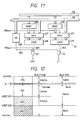
- Fig. 11 shows an embodiment of a portion of another but preferable bus controller 40 according to the present invention.
- This bus controller 40 includes an address register ARBT to be used for switching the data bus width and an address register AR3T to be used for changing the bus cycle, so that it executes two kinds of bus controls for changing the bus width and cycle dynamically and independently.
- This embodiment to be described is one which is prepared by eliminating the ROM 12 and the RAM 14 from the microcomputer 1 of Fig. 1(a).
- the single chip mode is eliminated, and the address areas IROM and IRAM of the ROM 12 and the RAM 14 at the memory map in the modes 1 and 2 are replaced by the external address area EX.
- the minimum extension modes 1 and 2 are made to belong to a common memory map
- the maximum extension modes 3 and 4 are made to belong to a common memory map.
- the modes 1 and 3 are used especially for the 8-bit interface, and the modes 2 and 4 can be interchanged between the 8- and 16- bit interfaces. As a result, the degree of freedom for the user to design the data processing system is improved.
- This bus controller 40 includes an 8-bit readable/writable byte area top register (ARBT) 405 and an 8-bit readable/writable 3-state area top register (AR3T) 406.
- ARBT 8-bit readable/writable byte area top register
- AR3T 8-bit readable/writable 3-state area top register
- the ARBT 405 is used in the modes 2 and 4 as an address register for setting the address of the boundary between the address space (or byte area) to be used as the 8-bit bus interface and the address space (or word area) to be used as the 16-bit bus interface.
- the ARBT 405 can be set at the unit of 64 Kbytes in the maximum extension mode 4 so as to store the higher 8 bits of the boundary address fed from the MPU 10 to the data bus DB.
- the ARBT 405 can be set at the unit of 4 Kbytes in the minimum extension mode 2 so as to store the higher 4 bits of the boundary address fed from the MPU 10 through the data bus DB.
- a multiplexer (MPX) 407 feeds a comparator (COMP) 408 with both the address data stored in the ARBT 405 and the address signal fed onto the address bus AB from the MPU 10.
- the aforementioned MPX 407 feeds the aforementioned COMP 408 with the 8-bit address data stored in the ARBT 405 and the higher 8 bits of the address signal on the address bus AB.
- the MPX 407 feeds the comparator with the 4-bit address in the ARBT 405 and the higher 4 bits of the address signal on the address bus AB.
- the aforementioned COMP 408 compares the higher 8 bits (or higher 4 bits) of the boundary address data fed from the aforementioned MPX 407 and the higher 8 bits (or higher 4 bits) of the address signal on the address bus AB to output a comparison result signal RE1 at the high level when the address signal on the address bus AB is higher than the boundary address stored in the ARBT 40.
- the aforementioned signal RE1 is fed to the first input of an OR Gate G1.
- the second input of the gate G1 is fed with a mode signal MD1 or MD3 indicating the minimum extension mode 1 or the maximum extension mode 3 outputted from the mode controller 30.
- the third input of the gate G1 is fed with the output signal RE2 of a detector 409.
- This detector 409 is linked to the address bus AB to detect the address signal, which corresponds to one of the various registers in the internal blocks 16, 18, 20, 22, 28, 36 and 40 indicated at R in the memory map, when the MPU 10 outputs it onto the address bus AB so as to access one of the registers, and feeds the output signal RE2 at the high level to the gate G1.
- the gate G1 outputs to the MPU 10 a 8-bit data address request signal CRS at the high level instructing the 8-bit bus interface.
- the MPU 10 is controlled to take the 8-bit interface.
- the MPU 10 is controlled to take the 8-bit interface even for the predetermined address area R in the microcomputer 1.
- the detector 409 can be designed by using the address registers RA and RB and the comparators CPA and CPB, for example, as shown in Fig. 2.
- the detector 409 may be exemplified by a circuit which is designed especially therefor by another method.
- the aforementioned AR3T 406 is an address register for setting an address indicating the boundary between the address space to be accessed in two states and the address space to be accessed in three states.
- the AR3T 406 can be set at the unit of 64 Kbytes in the maximum extension modes 3 and 4 so as to store the higher 8 bits at the address of the boundary transferred from the MPU 10 through the data bus DB.
- the AR3T 406 can be set at the unit of 4 Kbytes so as to store the higher 4 bits of the boundary address which is transferred from the MPU 10 through the data bus DB.
- the output of the AR3T 406 and the address data on the address bus are fed to the inputs of a multiplexer (MPX) 410 given a function like that of the foregoing MPX 407 and further to a comparator (COMP) 411.
- MPX multiplexer
- COMP comparator
- This comparator 411 compares the address data in the AR3T 406 and the address signal on the address bus AB to output a comparison result signal RE3 at the high level when the address signal on the address bus is higher than the address data in the AR3T 406.
- the signal RE3 is fed to the first input of an OR gate G2.
- the second input of the OR gate G2 is fed with the signal RE2 from the RD 409.
- the OR gate G2 outputs a 3-state bus access request signal 3T at the high level to the MPU 10 when it receives the signal RE2 at the high level or the signal RE3 at the high level.
- Fig. 12 shows one example of the address space in the maximum extension mode 4, which is set by using the bus controller of Fig. 11.
- the address space (AS1) higher than the address data A1 set in the ARBT 405 is used as the interface of the 8-bit data bus
- the address spaces (AS1 and AS2) higher than the address data A2 set in the AR3T 406 are used as the interfaces of 3-state bus cycle.
- the address space (AS1) is used as the interface of the 8-bit bus and the 3-state bus cycle
- the address space (AS2) is used as the interface of 16-bit bus and the 2-state bus cycle
- the address spaces (AS3 and AS4) are used as the interfaces of 16-bit bus and the 2-state cycle.
- the address spaces (R), i.e., the address spaces of the registers in the peripheral circuits 16, 18, 20, 22, 28, 36 and 40 are used as the interfaces of 3-bit bus and the 3-state cycles independently of the aforementioned ARBT 405 and AR3T 406.
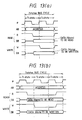
- Fig. 13(a) is a timing chart in case the address space (i.e., a portion in the AS4) in the microcomputer 1 to be used as the 2-state bus cycle and the 16-bit bus interface is accessed by the MPU 10.
- Letter R designates an internal read signal to be outputted from the MPU 10 and a read mode when it is at the low level.
- Letter W designates an internal write signal to be outputted from the MPU 10 and a write mode when it is at the low level.
- the 2-state bus cycle is construed to mean the bus cycle in which the access for the read/write operation is completed for two clocks in the system clock ⁇ , i.e., in the states T1 and T2.
- Fig. 13(b) is a timing chart in case the address space (R) in the microcomputer 1 to be used as the 3-state bus cycle and the 8-bit bus interface is to be accessed by the MPU 10. Since, in this case, the output signal RE2 of the detector RD of Fig. 11 is at the high level, both the outputs CRS and 3T of the gates G1 and G2 are raised to the high level. With this linkage and at the timing shown in Fig. 13(b), the MPU accesses the address in the address area (R). In Fig. 13(b), letter R designates the internal read signal, and letter W designates the internal write signal. Moreover, the 3-state bus cycle is construed to mean the bus cycle in which the access for the read/write operation is completed for three clocks in the system clock ⁇ , i.e., in the states T1, T2 and T3.
- the access to the address space (AS3) outside of the microcomputer 1, as shown in Fig. 12, is used as the 2-state bus cycle and the 16-bit bus interface,d and its timing chart is referred to the timing chart of the portion of the 16-bit interface of Figs. 9 and 10.
- the space (AS3) is assigned with the address of the high-speed memory such as the CMOS static RAM or the bipolar CMOS static RAM.
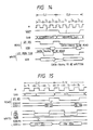
- Fig. 14 is a timing chart of a fist cycle CL1 in case the address space (AS2) outside of the microcomputer 1 to be used as the 3-state bus cycle and the 16-bit bus interface is to be accessed by the MPU 10.
- Fig. 14 also illustrates a bus cycle CL2 including a wait state Tw to be inserted by the wait state controller 36.
- This wait state controller 36 is activated when it receives the 3-state access request signal 3T at the high level outputted from the bus controller 40 of Fig. 11.
- the wait state controller 36 is activated, in the address state to be accessed in the 3-state bus cycle, to control the MPU 10 so that the wait states Tw of a predetermined number may be interposed between the states T2 and T3 in accordance with the operation mode.
- Fig. 14 letters WAIT are construed to indicate the voltage level of the external terminal WAIT , and the aforementioned wait state controller samples the voltage level of the external terminal WAIT at the breaking edge of the system clock ⁇ in the state T2.
- the wait state Tw is not interposed between the states T2 and T3, in case the sampled voltage is at the high level, but interposed between the states T2 and T3 in case the sample voltage is at the low level.
- CL2 There is indicated at CL2 the bus cycle in which one wait state Tw is interposed between the states T2 and T3 in the auto-wait mode.
- this address space (AS2) is assigned with the address of the ROM 7 or the like having a lower-speed address access time than that of the static RAM.
- Fig. 15 is a timing chart in case the address space (AS1) outside of the microcomputer 1 to be used as the 3-state bus cycle and the 8-bit bus interface is accessed by the MPU 10.
- AS1 address space
- the lower 8-bit external data D0 to D7 are read out in the bus cycle CL11, and the higher 8-bit data D8 to D15 are read out in the subsequent bus cycle CL12, until both of them are read out of the external device selected with the addresses n and n+1 and are sequentially introduced into the microcomputer 1.
- the lower 8-bit internal data ID0 to ID7 are outputted in the bus cycle CL11, and the higher 8-bit internal data ID8 to ID15 are outputted in the subsequent bus cycle CL12, until both of them are outputted to the lower external data bus SDB(L) from the microcomputer 1 and introduced into the external device selected at the addresses n and n+1.
- Fig. 12 shows the case in which the address data (A1) set in the ARBT 405 are smaller than the address data (A2) set in the AR3T 406.
- the address data (A1) are set in the AR3T 406 whereas the address data (A2) are set in the ARBT 405, the address space (AS2) is an area to be accessed in the 2-state bus cycle and with the 8-bit data bus interface.
- the address space (AS2) is accessed at the timing, as indicated as the 8-bit interface in Figs. 9 and 10.
- the bus cycle and size of the address space on the memory map can be set freely to some extent to improve the degree of freedom for the use to design it.
- the foregoing description is directed to the example in which the data terminals of the 8-bit external peripheral devices 4 and 5 are connected with the lower 8-bit external data bus SDB(L).
- the present invention should not be limited thereto, but the data terminals of the 8-bit external peripheral devices 4 and 5 may be connected with the higher external data bus SDB(H).
- the D0 to D15 of Figs. 5 and 6 are rewritten to D15 to D0
- the ID0 to ID15 of Figs. 5 and 6 are rewritten to ID15 to ID0.
- the lower external data bus SDB(L) is described to transfer the lower 8-bit internal data ID0 to ID7 at first and then the higher 8-bit internal data ID8 to ID15.
- the present invention should not be limited thereto but can be modified such that the IOB 50 is so controlled by the MPU 10 that the higher 8-bit internal data ID8 to ID15 may be transferred at first to the lower external data bus SDB(L) and that the lower 8-bit internal data ID0 to ID7 may then be transferred to the lower external data bus SDB(L).
- the structures of Figs. 10 to 15 may also be modified in the aforementioned manners.
- the present invention may be used in not only the microprocessor having the internal 16-bit structure but also a variety of general-purpose microprocessors having an 8- or 32-bit structure or a special processor.
- a specific address area is addressed by the internal registers, and this access to the specific address area is acknowledged so that the data bus width is accordingly changed dynamically.
- the microprocessor itself is enabled acknowledge whether the address is the designated address or the set specific address area, to change the bus width accordingly at a high speed and for general-purpose properties.
Landscapes
- Engineering & Computer Science (AREA)
- Theoretical Computer Science (AREA)
- General Engineering & Computer Science (AREA)
- Physics & Mathematics (AREA)
- General Physics & Mathematics (AREA)
- Computer Hardware Design (AREA)
- Microcomputers (AREA)
- Bus Control (AREA)
Applications Claiming Priority (2)
| Application Number | Priority Date | Filing Date | Title |
|---|---|---|---|
| JP235446/89 | 1989-09-11 | ||
| JP1235446A JPH0398145A (ja) | 1989-09-11 | 1989-09-11 | マイクロプロセッサ |
Publications (2)
| Publication Number | Publication Date |
|---|---|
| EP0417707A2 true EP0417707A2 (de) | 1991-03-20 |
| EP0417707A3 EP0417707A3 (en) | 1992-01-08 |
Family
ID=16986234
Family Applications (1)
| Application Number | Title | Priority Date | Filing Date |
|---|---|---|---|
| EP19900117417 Withdrawn EP0417707A3 (en) | 1989-09-11 | 1990-09-10 | Microcomputer with address registers for dynamic bus control |
Country Status (4)
| Country | Link |
|---|---|
| US (2) | US5341481A (de) |
| EP (1) | EP0417707A3 (de) |
| JP (1) | JPH0398145A (de) |
| KR (1) | KR0160128B1 (de) |
Cited By (6)
| Publication number | Priority date | Publication date | Assignee | Title |
|---|---|---|---|---|
| EP0559939A1 (de) * | 1992-03-11 | 1993-09-15 | Siemens Nixdorf Informationssysteme Aktiengesellschaft | Schaltungsanordnung zur Überwachung von Zugriffen auf einen vorgegebenen Speicherbereich eines Speichers |
| EP0597441A1 (de) * | 1992-11-09 | 1994-05-18 | Kabushiki Kaisha Toshiba | Mikroprozessor mit Busbreite-Wechselfunktion |
| JP2002528786A (ja) * | 1998-08-24 | 2002-09-03 | マイクロユニティ システムズ エンジニアリング インコーポレイテッド | ワイド・オペランド・アーキテクチャを含むシステムおよび方法 |
| JP2007531072A (ja) * | 2003-12-19 | 2007-11-01 | マイクロユニティ システムズ エンジニアリング インコーポレイテッド | プログラム可能なプロセッサ及び拡張演算を伴う方法 |
| US7818548B2 (en) | 1995-08-16 | 2010-10-19 | Microunity Systems Engineering, Inc. | Method and software for group data operations |
| US7849291B2 (en) | 1995-08-16 | 2010-12-07 | Microunity Systems Engineering, Inc. | Method and apparatus for performing improved group instructions |
Families Citing this family (30)
| Publication number | Priority date | Publication date | Assignee | Title |
|---|---|---|---|---|
| EP0444711A3 (en) * | 1990-03-02 | 1994-07-20 | Fujitsu Ltd | Bus control system in a multi-processor system |
| JPH0520197A (ja) * | 1991-07-09 | 1993-01-29 | Hitachi Ltd | 記憶管理システム及びマイクロプロセツサ |
| JP2718292B2 (ja) * | 1991-07-24 | 1998-02-25 | 日本電気株式会社 | マイクロプロセッサ |
| JP2744154B2 (ja) * | 1991-10-24 | 1998-04-28 | 株式会社東芝 | バスシステム |
| JP2836321B2 (ja) * | 1991-11-05 | 1998-12-14 | 三菱電機株式会社 | データ処理装置 |
| JPH06150023A (ja) * | 1992-11-06 | 1994-05-31 | Hitachi Ltd | マイクロコンピュータ及びマイクロコンピュータシステム |
| JP3216931B2 (ja) * | 1993-01-13 | 2001-10-09 | 日本電気株式会社 | バスサイジングを有するマイクロプロセッサ |
| JP3904244B2 (ja) * | 1993-09-17 | 2007-04-11 | 株式会社ルネサステクノロジ | シングル・チップ・データ処理装置 |
| JP3060812B2 (ja) * | 1993-12-27 | 2000-07-10 | 日本電気株式会社 | 情報処理装置 |
| US6735683B2 (en) | 1994-09-14 | 2004-05-11 | Hitachi, Ltd. | Single-chip microcomputer with hierarchical internal bus structure having data and address signal lines coupling CPU with other processing elements |
| US5867726A (en) * | 1995-05-02 | 1999-02-02 | Hitachi, Ltd. | Microcomputer |
| US5689659A (en) * | 1995-10-30 | 1997-11-18 | Motorola, Inc. | Method and apparatus for bursting operand transfers during dynamic bus sizing |
| US5854944A (en) * | 1996-05-09 | 1998-12-29 | Motorola, Inc. | Method and apparatus for determining wait states on a per cycle basis in a data processing system |
| US6253302B1 (en) * | 1996-08-29 | 2001-06-26 | Intel Corporation | Method and apparatus for supporting multiple overlapping address spaces on a shared bus |
| US6427179B1 (en) * | 1997-10-01 | 2002-07-30 | Globespanvirata, Inc. | System and method for protocol conversion in a communications system |
| US6418493B1 (en) * | 1997-12-29 | 2002-07-09 | Intel Corporation | Method and apparatus for robust addressing on a dynamically configurable bus |
| ATE557342T1 (de) | 1998-08-24 | 2012-05-15 | Microunity Systems Eng | Prozessor und verfahren zur matrixmultiplikation mit einem breiten operand |
| US7932911B2 (en) | 1998-08-24 | 2011-04-26 | Microunity Systems Engineering, Inc. | Processor for executing switch and translate instructions requiring wide operands |
| KR100605902B1 (ko) * | 1999-12-11 | 2006-08-01 | 삼성전자주식회사 | 통신시스템에서 제어버스 억세스 장치 및 방법 |
| KR100475125B1 (ko) * | 2003-06-21 | 2005-03-14 | 삼성전자주식회사 | 데이터 버스 폭 변경이 자유로운 이동형 저장 장치 및이에 대한 데이터 버스 폭 설정 방법 |
| US7136987B2 (en) * | 2004-03-30 | 2006-11-14 | Intel Corporation | Memory configuration apparatus, systems, and methods |
| US20070143579A1 (en) * | 2005-12-19 | 2007-06-21 | King Billion Electronics Co. Ltd. | Integrated data processor |
| US8654868B2 (en) * | 2006-04-18 | 2014-02-18 | Qualcomm Incorporated | Offloaded processing for wireless applications |
| US8289159B2 (en) * | 2006-04-26 | 2012-10-16 | Qualcomm Incorporated | Wireless localization apparatus and method |
| AR060670A1 (es) * | 2006-04-26 | 2008-07-02 | Qualcomm Inc | Distribucion dinamica de funcionalidad y administracion de recursos en un dispositivo |
| US8406794B2 (en) | 2006-04-26 | 2013-03-26 | Qualcomm Incorporated | Methods and apparatuses of initiating communication in wireless networks |
| US7822899B2 (en) | 2007-03-08 | 2010-10-26 | Renesas Electronics Corporation | Data processor and control system |
| JP4994254B2 (ja) * | 2007-03-08 | 2012-08-08 | ルネサスエレクトロニクス株式会社 | データプロセッサ及び制御システム |
| JP5441219B2 (ja) * | 2009-06-26 | 2014-03-12 | ルネサスエレクトロニクス株式会社 | 半導体装置及びシリアルインタフェース回路 |
| US9785565B2 (en) | 2014-06-30 | 2017-10-10 | Microunity Systems Engineering, Inc. | System and methods for expandably wide processor instructions |
Family Cites Families (33)
| Publication number | Priority date | Publication date | Assignee | Title |
|---|---|---|---|---|
| US4363091A (en) * | 1978-01-31 | 1982-12-07 | Intel Corporation | Extended address, single and multiple bit microprocessor |
| US4447878A (en) * | 1978-05-30 | 1984-05-08 | Intel Corporation | Apparatus and method for providing byte and word compatible information transfers |
| DE3177233D1 (de) * | 1980-03-19 | 1990-12-20 | Toshiba Kawasaki Kk | Datenverarbeitungssystem. |
| JPS56140459A (en) * | 1980-04-04 | 1981-11-02 | Hitachi Ltd | Data processing system |
| DE3265361D1 (en) * | 1981-07-10 | 1985-09-19 | Siemens Ag Albis | Bus system |
| DE3176950D1 (en) * | 1981-08-12 | 1989-01-12 | Ibm | Extended addressing apparatus and method for direct storage access devices |
| US4580213A (en) * | 1982-07-07 | 1986-04-01 | Motorola, Inc. | Microprocessor capable of automatically performing multiple bus cycles |
| US4590556A (en) * | 1983-01-17 | 1986-05-20 | Tandy Corporation | Co-processor combination |
| US4893235A (en) * | 1983-10-03 | 1990-01-09 | Digital Equipment Corporation | Central processing unit for a digital computer |
| KR900007564B1 (ko) * | 1984-06-26 | 1990-10-15 | 모토로라 인코포레이티드 | 동적 버스를 갖는 데이터 처리기 |
| JPS61139866A (ja) * | 1984-12-11 | 1986-06-27 | Toshiba Corp | マイクロプロセツサ |
| US4683534A (en) * | 1985-06-17 | 1987-07-28 | Motorola, Inc. | Method and apparatus for interfacing buses of different sizes |
| JPS6226561A (ja) * | 1985-07-26 | 1987-02-04 | Toshiba Corp | パ−ソナルコンピユ−タ |
| JPS6275867A (ja) * | 1985-09-30 | 1987-04-07 | Toshiba Corp | デ−タ転送制御方式 |
| US4752871A (en) * | 1985-09-30 | 1988-06-21 | Motorola, Inc. | Single-chip microcomputer having a program register for controlling two EEPROM arrays |
| US4831514A (en) * | 1986-02-14 | 1989-05-16 | Dso "Izot" | Method and device for connecting a 16-bit microprocessor to 8-bit modules |
| JPH0778780B2 (ja) * | 1986-04-02 | 1995-08-23 | 日本電気株式会社 | バス幅制御装置 |
| JPS62232061A (ja) * | 1986-04-02 | 1987-10-12 | Casio Comput Co Ltd | デ−タ転送処理装置 |
| US5014186A (en) * | 1986-08-01 | 1991-05-07 | International Business Machines Corporation | Data-processing system having a packet transfer type input/output system |
| US5109492A (en) * | 1986-09-19 | 1992-04-28 | Hitachi, Ltd. | Microprocessor which terminates bus cycle when access address falls within a predetermined processor system address space |
| JPS63261445A (ja) * | 1987-04-20 | 1988-10-28 | Hitachi Ltd | メモリ制御方式 |
| JPS63296158A (ja) * | 1987-05-28 | 1988-12-02 | Canon Inc | 情報処理装置 |
| JPS6431252A (en) * | 1987-07-28 | 1989-02-01 | Nec Corp | Data bus width transformer |
| GB2211326B (en) * | 1987-10-16 | 1991-12-11 | Hitachi Ltd | Address bus control apparatus |
| US4965723A (en) * | 1987-10-23 | 1990-10-23 | Digital Equipment Corporation | Bus data path control scheme |
| JPH01248256A (ja) * | 1988-03-30 | 1989-10-03 | Toshiba Corp | 入出力制御方式 |
| US5045998A (en) * | 1988-05-26 | 1991-09-03 | International Business Machines Corporation | Method and apparatus for selectively posting write cycles using the 82385 cache controller |
| DE3823720A1 (de) * | 1988-07-13 | 1990-01-18 | Grote & Hartmann | Verfahren und vorrichtung zum maschinellen aufbringen von dichtungsstopfen auf elektrische leitungen |
| GB2222471B (en) * | 1988-08-29 | 1992-12-09 | Mitsubishi Electric Corp | Ic card with switchable bus structure |
| JPH02141856A (ja) * | 1988-11-24 | 1990-05-31 | Hitachi Ltd | Cpuボードのデータバス変換装置 |
| US5109490A (en) * | 1989-01-13 | 1992-04-28 | International Business Machines Corporation | Data transfer using bus address lines |
| US5214767A (en) * | 1989-02-07 | 1993-05-25 | Compaq Computer Corp. | Full address and odd boundary direct memory access controller which determines address size by counting the input address bytes |
| US5274795A (en) * | 1989-08-18 | 1993-12-28 | Schlumberger Technology Corporation | Peripheral I/O bus and programmable bus interface for computer data acquisition |
-
1989
- 1989-09-11 JP JP1235446A patent/JPH0398145A/ja active Pending
-
1990
- 1990-09-10 EP EP19900117417 patent/EP0417707A3/en not_active Withdrawn
- 1990-09-11 KR KR1019900014320A patent/KR0160128B1/ko not_active Expired - Fee Related
-
1993
- 1993-04-28 US US08/055,230 patent/US5341481A/en not_active Expired - Fee Related
-
1995
- 1995-05-02 US US08/437,152 patent/US5493656A/en not_active Expired - Fee Related
Cited By (10)
| Publication number | Priority date | Publication date | Assignee | Title |
|---|---|---|---|---|
| EP0559939A1 (de) * | 1992-03-11 | 1993-09-15 | Siemens Nixdorf Informationssysteme Aktiengesellschaft | Schaltungsanordnung zur Überwachung von Zugriffen auf einen vorgegebenen Speicherbereich eines Speichers |
| EP0597441A1 (de) * | 1992-11-09 | 1994-05-18 | Kabushiki Kaisha Toshiba | Mikroprozessor mit Busbreite-Wechselfunktion |
| US5613078A (en) * | 1992-11-09 | 1997-03-18 | Kabushiki Kaisha Toshiba | Microprocessor and microprocessor system with changeable effective bus width |
| US7818548B2 (en) | 1995-08-16 | 2010-10-19 | Microunity Systems Engineering, Inc. | Method and software for group data operations |
| US7849291B2 (en) | 1995-08-16 | 2010-12-07 | Microunity Systems Engineering, Inc. | Method and apparatus for performing improved group instructions |
| US7987344B2 (en) | 1995-08-16 | 2011-07-26 | Microunity Systems Engineering, Inc. | Multithreaded programmable processor and system with partitioned operations |
| US8001360B2 (en) | 1995-08-16 | 2011-08-16 | Microunity Systems Engineering, Inc. | Method and software for partitioned group element selection operation |
| US8117426B2 (en) | 1995-08-16 | 2012-02-14 | Microunity Systems Engineering, Inc | System and apparatus for group floating-point arithmetic operations |
| JP2002528786A (ja) * | 1998-08-24 | 2002-09-03 | マイクロユニティ システムズ エンジニアリング インコーポレイテッド | ワイド・オペランド・アーキテクチャを含むシステムおよび方法 |
| JP2007531072A (ja) * | 2003-12-19 | 2007-11-01 | マイクロユニティ システムズ エンジニアリング インコーポレイテッド | プログラム可能なプロセッサ及び拡張演算を伴う方法 |
Also Published As
| Publication number | Publication date |
|---|---|
| US5493656A (en) | 1996-02-20 |
| KR0160128B1 (ko) | 1998-12-15 |
| US5341481A (en) | 1994-08-23 |
| KR910006856A (ko) | 1991-04-30 |
| EP0417707A3 (en) | 1992-01-08 |
| JPH0398145A (ja) | 1991-04-23 |
Similar Documents
| Publication | Publication Date | Title |
|---|---|---|
| EP0417707A2 (de) | Mikrorechner mit Adressenregistern für dynamische Bussteuerung | |
| US6070205A (en) | High-speed processor system having bus arbitration mechanism | |
| US6216191B1 (en) | Field programmable gate array having a dedicated processor interface | |
| EP0428111A2 (de) | Datenübertragungssteuerungsverfahren und Datenprozessor, der dieses verwendet | |
| JPH039492B2 (de) | ||
| US5325521A (en) | Wait control device | |
| US5056011A (en) | Direct memory access controller with expedited error control | |
| KR920008448B1 (ko) | 데이터 프로세서 | |
| US5828891A (en) | Multilevel interrupt device | |
| US5561819A (en) | Computer system selecting byte lane for a peripheral device during I/O addressing technique of disabling non-participating peripherals by driving an address within a range on the local bus in a DMA controller | |
| KR100375233B1 (ko) | 전송될 데이터 길이 값에 따라 전송 모드가 유동적으로변환되는 직접 메모리 억세스 컨트롤러 | |
| US7908416B2 (en) | Data processing unit and bus arbitration unit | |
| EP0338564B1 (de) | Verfahren zur Mikroprogrammabzweigung und die Mikrofolgekontrolleinheit, die Gebrauch vom Verfahren macht | |
| US7310717B2 (en) | Data transfer control unit with selectable transfer unit size | |
| US5043935A (en) | Data transfer system for rearranging data units using intermediate temporary registers | |
| JP2854474B2 (ja) | バス使用要求調停装置 | |
| US20020019917A1 (en) | Data transfer apparatus and microcomputer | |
| JPH11259417A (ja) | バスアクセス方式およびバスアクセス制御装置 | |
| JPH05328734A (ja) | モータコントロール回路内蔵マイクロコンピュータ | |
| KR100238313B1 (ko) | Cpu와 주변장치 사이의 인터페이스 장치 및 방법 | |
| JP3611049B2 (ja) | 内部レジスタ回路 | |
| JP3264921B2 (ja) | データ転送制御装置 | |
| JP4642398B2 (ja) | 共有バス調停システム | |
| KR200142909Y1 (ko) | 입출력 인터페이스 장치 | |
| KR940005003Y1 (ko) | 직접 메모리 억세스 시스템 |
Legal Events
| Date | Code | Title | Description |
|---|---|---|---|
| PUAI | Public reference made under article 153(3) epc to a published international application that has entered the european phase |
Free format text: ORIGINAL CODE: 0009012 |
|
| AK | Designated contracting states |
Kind code of ref document: A2 Designated state(s): DE FR GB IT |
|
| PUAL | Search report despatched |
Free format text: ORIGINAL CODE: 0009013 |
|
| AK | Designated contracting states |
Kind code of ref document: A3 Designated state(s): DE FR GB IT |
|
| 17P | Request for examination filed |
Effective date: 19920629 |
|
| 17Q | First examination report despatched |
Effective date: 19941118 |
|
| STAA | Information on the status of an ep patent application or granted ep patent |
Free format text: STATUS: THE APPLICATION IS DEEMED TO BE WITHDRAWN |
|
| 18D | Application deemed to be withdrawn |
Effective date: 19971029 |