EP0414204A2 - Substrat d'interconnexion à multicouche et dispositif semi-conducteur à circuit intégré comprenant ce substrat - Google Patents
Substrat d'interconnexion à multicouche et dispositif semi-conducteur à circuit intégré comprenant ce substrat Download PDFInfo
- Publication number
- EP0414204A2 EP0414204A2 EP90115984A EP90115984A EP0414204A2 EP 0414204 A2 EP0414204 A2 EP 0414204A2 EP 90115984 A EP90115984 A EP 90115984A EP 90115984 A EP90115984 A EP 90115984A EP 0414204 A2 EP0414204 A2 EP 0414204A2
- Authority
- EP
- European Patent Office
- Prior art keywords
- power supply
- layers
- signal
- connection terminal
- interconnecting
- Prior art date
- Legal status (The legal status is an assumption and is not a legal conclusion. Google has not performed a legal analysis and makes no representation as to the accuracy of the status listed.)
- Withdrawn
Links
Images


Classifications
-
- H—ELECTRICITY
- H01—ELECTRIC ELEMENTS
- H01L—SEMICONDUCTOR DEVICES NOT COVERED BY CLASS H10
- H01L23/00—Details of semiconductor or other solid state devices
- H01L23/52—Arrangements for conducting electric current within the device in operation from one component to another, i.e. interconnections, e.g. wires, lead frames
- H01L23/538—Arrangements for conducting electric current within the device in operation from one component to another, i.e. interconnections, e.g. wires, lead frames the interconnection structure between a plurality of semiconductor chips being formed on, or in, insulating substrates
- H01L23/5385—Assembly of a plurality of insulating substrates
-
- H—ELECTRICITY
- H05—ELECTRIC TECHNIQUES NOT OTHERWISE PROVIDED FOR
- H05K—PRINTED CIRCUITS; CASINGS OR CONSTRUCTIONAL DETAILS OF ELECTRIC APPARATUS; MANUFACTURE OF ASSEMBLAGES OF ELECTRICAL COMPONENTS
- H05K3/00—Apparatus or processes for manufacturing printed circuits
- H05K3/46—Manufacturing multilayer circuits
-
- H—ELECTRICITY
- H01—ELECTRIC ELEMENTS
- H01L—SEMICONDUCTOR DEVICES NOT COVERED BY CLASS H10
- H01L23/00—Details of semiconductor or other solid state devices
- H01L23/48—Arrangements for conducting electric current to or from the solid state body in operation, e.g. leads, terminal arrangements ; Selection of materials therefor
- H01L23/50—Arrangements for conducting electric current to or from the solid state body in operation, e.g. leads, terminal arrangements ; Selection of materials therefor for integrated circuit devices, e.g. power bus, number of leads
-
- H—ELECTRICITY
- H01—ELECTRIC ELEMENTS
- H01L—SEMICONDUCTOR DEVICES NOT COVERED BY CLASS H10
- H01L23/00—Details of semiconductor or other solid state devices
- H01L23/52—Arrangements for conducting electric current within the device in operation from one component to another, i.e. interconnections, e.g. wires, lead frames
- H01L23/538—Arrangements for conducting electric current within the device in operation from one component to another, i.e. interconnections, e.g. wires, lead frames the interconnection structure between a plurality of semiconductor chips being formed on, or in, insulating substrates
- H01L23/5383—Multilayer substrates
-
- H—ELECTRICITY
- H01—ELECTRIC ELEMENTS
- H01L—SEMICONDUCTOR DEVICES NOT COVERED BY CLASS H10
- H01L25/00—Assemblies consisting of a plurality of individual semiconductor or other solid state devices ; Multistep manufacturing processes thereof
- H01L25/03—Assemblies consisting of a plurality of individual semiconductor or other solid state devices ; Multistep manufacturing processes thereof all the devices being of a type provided for in the same subgroup of groups H01L27/00 - H01L33/00, or in a single subclass of H10K, H10N, e.g. assemblies of rectifier diodes
- H01L25/04—Assemblies consisting of a plurality of individual semiconductor or other solid state devices ; Multistep manufacturing processes thereof all the devices being of a type provided for in the same subgroup of groups H01L27/00 - H01L33/00, or in a single subclass of H10K, H10N, e.g. assemblies of rectifier diodes the devices not having separate containers
- H01L25/065—Assemblies consisting of a plurality of individual semiconductor or other solid state devices ; Multistep manufacturing processes thereof all the devices being of a type provided for in the same subgroup of groups H01L27/00 - H01L33/00, or in a single subclass of H10K, H10N, e.g. assemblies of rectifier diodes the devices not having separate containers the devices being of a type provided for in group H01L27/00
- H01L25/0652—Assemblies consisting of a plurality of individual semiconductor or other solid state devices ; Multistep manufacturing processes thereof all the devices being of a type provided for in the same subgroup of groups H01L27/00 - H01L33/00, or in a single subclass of H10K, H10N, e.g. assemblies of rectifier diodes the devices not having separate containers the devices being of a type provided for in group H01L27/00 the devices being arranged next and on each other, i.e. mixed assemblies
-
- H—ELECTRICITY
- H01—ELECTRIC ELEMENTS
- H01L—SEMICONDUCTOR DEVICES NOT COVERED BY CLASS H10
- H01L2224/00—Indexing scheme for arrangements for connecting or disconnecting semiconductor or solid-state bodies and methods related thereto as covered by H01L24/00
- H01L2224/01—Means for bonding being attached to, or being formed on, the surface to be connected, e.g. chip-to-package, die-attach, "first-level" interconnects; Manufacturing methods related thereto
- H01L2224/10—Bump connectors; Manufacturing methods related thereto
- H01L2224/15—Structure, shape, material or disposition of the bump connectors after the connecting process
- H01L2224/16—Structure, shape, material or disposition of the bump connectors after the connecting process of an individual bump connector
- H01L2224/161—Disposition
- H01L2224/16151—Disposition the bump connector connecting between a semiconductor or solid-state body and an item not being a semiconductor or solid-state body, e.g. chip-to-substrate, chip-to-passive
- H01L2224/16221—Disposition the bump connector connecting between a semiconductor or solid-state body and an item not being a semiconductor or solid-state body, e.g. chip-to-substrate, chip-to-passive the body and the item being stacked
- H01L2224/16225—Disposition the bump connector connecting between a semiconductor or solid-state body and an item not being a semiconductor or solid-state body, e.g. chip-to-substrate, chip-to-passive the body and the item being stacked the item being non-metallic, e.g. insulating substrate with or without metallisation
-
- H—ELECTRICITY
- H01—ELECTRIC ELEMENTS
- H01L—SEMICONDUCTOR DEVICES NOT COVERED BY CLASS H10
- H01L2924/00—Indexing scheme for arrangements or methods for connecting or disconnecting semiconductor or solid-state bodies as covered by H01L24/00
- H01L2924/01—Chemical elements
- H01L2924/01078—Platinum [Pt]
-
- H—ELECTRICITY
- H01—ELECTRIC ELEMENTS
- H01L—SEMICONDUCTOR DEVICES NOT COVERED BY CLASS H10
- H01L2924/00—Indexing scheme for arrangements or methods for connecting or disconnecting semiconductor or solid-state bodies as covered by H01L24/00
- H01L2924/15—Details of package parts other than the semiconductor or other solid state devices to be connected
- H01L2924/151—Die mounting substrate
- H01L2924/153—Connection portion
- H01L2924/1531—Connection portion the connection portion being formed only on the surface of the substrate opposite to the die mounting surface
- H01L2924/15312—Connection portion the connection portion being formed only on the surface of the substrate opposite to the die mounting surface being a pin array, e.g. PGA
-
- H—ELECTRICITY
- H01—ELECTRIC ELEMENTS
- H01L—SEMICONDUCTOR DEVICES NOT COVERED BY CLASS H10
- H01L2924/00—Indexing scheme for arrangements or methods for connecting or disconnecting semiconductor or solid-state bodies as covered by H01L24/00
- H01L2924/30—Technical effects
- H01L2924/301—Electrical effects
- H01L2924/3011—Impedance
Definitions
- the present invention relates to a multilayer interconnection substrate and a semiconductor integrated circuit device using the same.
- the multilayer interconnection substrate is suitably but not exclusively used for mounting a combination of circuit components, such as semiconductors, having a variety of supply voltages, number of pins and sizes.
- the multilayer interconnection substrate is used for mounting semiconductor components such as large scale integrated (LSI) circuit.
- the multilayer interconnection substrate has ceramic layers laminated each other, each layer having a conductor layer printed on it. Through holes are formed through layers to interconnect conductors.
- the multilayer interconnection substrate has one major surface serving as a component mounting surface and the other major surface serving as a pin connection surface.
- the conductor layers of the multilayer interconnection substrate includes signal layers and power supply layers, the former transmitting signals and the latter performing power supplying or impedance matching.
- Typical structures of the conventional multilayer interconnection substrate are disclosed in Nikkei Science, Japan, Vol.13, No.9 (1983), pp.13-25, and 19th Design Automation Conference Paper 9.4, pp.96-103 "pp99 Figure 5", for example.
- the multilayer interconnection substrates are fabricated as follows: materials are mixed and formed into sheets, so called green sheets; the green sheets are punched to form through holes: then, a conductor pattern, such as a pattern for a power supply layer, a signal layer, or the like, is imprinted on each green sheet with a print mask having a predetermined pattern; these green sheets are laminated and sinterd; finally the laminate is subjected to a finish treatment such as plating.
- Patterns of the power supply layers and the signal layers depend on the kind and the layout of the LSI circuits mounted.
- the patterns of the power supply layers and the signal layers must be changed, for example, when semiconductor components which are different in supply voltage, the number of pins, size, etc are mounted, or when the arrangement of the semiconductor components is changed. For this reason, a new multilayer interconnection substrate having different patterns of power supply layers and signal layers must be prepared for a different combination of LSI circuits or a different layout.
- Such multilayer interconnection substrates are produced on a many-kind-small-amount production basis, and hence many print masks with different conductor patterns must be prepared.
- the fabrication of the multilayer interconnection substrate according to the prior art requires many manhours.
- input/output pins of the multilayer interconnection substrate are changed in position according to modifications in conductor patterns and shifts of through holes. According to circumstances, there might be a need to modify the pattern of the printed wiring board on which the multilayer interconnection substrate is mounted.
- the present invention provides a multilayer interconnection substrate including: signal layers; power supply layers; at least one power supply matching layer provided to correspond in voltage to components to be mounted; and insulating layers electrically insulating the layers from each other.
- the at least one power supply matching layer is provided in the form of a bus-bar layer which is layered above both the signal layers and the power supply layers and close to the component mounting surface, so that the components may be connected to the power supply layers of the desired voltages through the bus-bar layer or layers of said desired voltages, respectively.
- a multilayer interconnection substrate of the type including a component mounting surface comprising: signal layers; power supply layers; at least one power supply matching layer, provided above both the signal layers and the power supply layers and close to the component mounting surface, the power supply matching layer corresponding in voltage to a component to be mounted to the component mounting surface; insulating layers for electrically insulating the signal layers, the power supply layers and the power supply matching layer from each other; the signal layers, the power supply layers, the power supply matching layer and the insulating layers being laminated to form the substrate; component connection terminal means, disposed on the component mounting surface for connection to the components; the component connection terminal means including component power supply terminals; external connection terminal means disposed on another surface of the multilayer interconnection substrate; the external connection terminal means including external power supply terminals; and interconnecting means; the interconnecting means including: first power supply interconnection means for interconnecting the power supply matching layer to corresponding component power supply terminals; second power supply interconnection means for interconnecting the power supply matching layer
- a power matching layer is layered above both the signal layers and the power supply layers and close to the component mounting surface.
- a semiconductor component which is different in power supply position from usual semiconductors is mounted to the component mounting surface
- misalignment is caused in the power supply position of the semiconductor component, which is absorbed by the power supply matching layer.
- the misalignment is also absorbed by the power supply matching layer when the mounting layout of the semiconductor component is modified.
- changes in power supply position due to modifications in components to be mounted and in layout exert no influence on the positions of interconnection means in layers below the power supply matching layer: the signal layers and the power supply layers.
- the present invention is capable of reducing the manhour necessary for each of the design, fabrication of masks, the production process, inspection of the product, and other treatments.
- the signal layers, the power supply layers and the power supply matching layer may have each a corresponding conductor pattern which is sandwiched between adjacent insulating layers; and the interconnecting means may comprise through holes formed through at least some of the insulating layers.
- a multilayer interconnection substrate having component mounting surfaces for mounting components thereon, comprising: signal layers; power supply layers; at least two power supply matching layers which are respectively layered above and below both the signal layers and the power supply layers and close to the component mounting surfaces; each power supply matching layer being provided to correspond to respective voltages of the components to be mounted to the component mounting surfaces; insulating layers for electrically insulating the signal layers, the power supply layers and the power supply matching layer from each other; said signal layers, said power supply layers, said power supply matching layers and the insulating layers being superposed into a laminate; component connection terminal means, mounted to the component mounting surfaces, respectively, for connection to the components; said component connection terminal means including component power supply terminals; external connection terminal means mounted to another surface of the multilayer interconnection substrate; said external connection terminal means including external power supply terminals; and interconnecting means including: first power supply interconnection means for interconnecting said power supply matching layers to corresponding component power supply terminals; second power supply interconnection means for interconnecting the power
- an external connector is provided to another, side surface of the multilayer interconnection terminal for connection with the external power supply terminals and the external signal terminals.
- components to be mounted to the component mounting surface may include semiconductor chips such as LSI chips.
- the component connection terminal means comprises signal terminals; the external connection terminal means comprises external signal terminals; and the interconnecting means comprises: first signal interconnection means for interconnecting the signal terminals of the component connection terminal means to corresponding signal layers; and second signal interconnection means for interconnecting the external signal terminals of the external connection terminal means to corresponding signal layers.
- I/O Input/output
- the component connection terminal means comprises signal terminals.
- the external connection terminal means comprises external signal terminals.
- the interconnecting means comprises: first signal interconnection means for interconnecting the signal terminals of the component connection terminal means to corresponding signal layers; and second signal interconnection means for interconnecting the external signal terminals of the external connection terminal means to corresponding signal layers.
- Both the signal terminals and the power supply terminals of the first component connection terminal means are separated in groups, each group being arranged at a corresponding chip site on the component mounting surface, the chip site being adapted to have a corresponding component mounted thereat.
- the first power supply interconnection means and the first signal interconnection means may have each the same arrangement pattern as to every group of component connection terminal means.
- the present invention may be applied to a chip carrier.
- the chip carrier comprises at least one power supply matching layer corresponding in voltage to a semiconductor chip and insulating layers sandwiching the power supply matching layer.
- the insulating layers and the power supply matching layer are laminated.
- Chip connection terminal means is disposed on one surface of the chip carrier for connection to the semiconductor chip, the chip connection terminal means including chip power supply terminals.
- Substrate connection terminal means is disposed on the other surface of the chip carrier for connecting to a multilayer interconnection substrate.
- the substrate connection terminal means includes substrate power supply terminals.
- Interconnecting means is provided to interconnect each of both the chip power supply terminals and the substrate power supply terminals to a corresponding power supply matching layer.
- a semiconductor integrated circuit may be built by mounting a semiconductor chip on the multilayer interconnection substrate as stated above with or without the chip carrier already described.
- reference numerals 1, 2 and 3 indicate semiconductor chips, which have different supply voltages at power supply bumps on their substrate interconnection surfaces.
- Reference numeral 4 designates a multilayer interconnection substrate, 5 input/output (I/O) pins for supplying power, 6 I/O pins for signals, 7 an enlarged layer, 8 power supply matching layers in the form of bus-bar layers, 9 signal layers, and 10 power supply layers.
- Each of the power supply layers 10 serves an impedance matching layer as well as a power supply layer.
- Reference numerals 11, 12, 13 and 14 indicate through holes constituting interconnection paths: 11 designates signal through holes connected to corresponding semiconductor chips 1, 2 and 3; 12 signal through holes connected to corresponding power supply I/O pins 5 and signal I/O pins 6; 13 power supply through holes connected to corresponding I/O pins, respectively; and 14 power supplying through holes connected to corresponding semiconductor chips.
- the multilayer interconnection substrate 4 includes the enlarged layer 7, power supply matching layers 8 provided in the form of bus-bar layers, signal layers 9, power supply layers 10 and through holes 11, 12, 13, and 14 connecting these elements.
- the enlarged layer 7 is an interconnecting layer to match corresponding through holes 11 and bumps 16 which are connected to semiconductor chips to be mounted.
- the enlarged layer 7 may be omitted.
- the power supply matching layers 8 are provided to correspond to voltages of the semiconductor chips 1 to 3 to be mounted. That is, when three voltages are needed for these semiconductor chips 1 to 3, three layers of power supply matching layers 8 are formed. Thus, the power supply matching layers 8 are designed to correspond to various layouts and semiconductor components to be mounted.
- Each of the signal layers 9 is used for transmitting signals and is connected to a corresponding signal through hole 12 and signal through hole 11 to transmit a signal.
- one signal layer 9 is provided for every power supply layer 10, but two signal layers 9 may be formed for every power supply layer 10.
- the interconnection patterns of the signal layers 9 are designed according to the kinds of semiconductor components to be mounted and a layout thereof.
- the power supply layers 10 are formed so that adjacent power supply layers 10 may sandwich one signal layer 9.
- the power supply layers 10 serve to supply electric power and to match impedance.
- the power supply layers 10 are provided to correspond to signal layers 9. It is to be noted that the power supply layers 10 each have a fixed pattern for connection with or non-connection with to the power supply through holes 13 as well as a fixed pattern for connection with or non-connection with the through holes 11 and 12. Accordingly, it suffices to use several predetermined conductor patterns of each power supply layer 10 irrespective of sorts of semiconductor components to be mounted and layouts.
- each power supply layer 10 is formed, for example, as shown in FIG. 3 which is a view taken along the line A-A in FIG. 1.
- FIG. 3 hatching shows conductors formed.
- the hollow circles indicate through holes which pass without making electrical contact with the conductors whereas the solid circles are through holes which electrically connect to the conductors.
- the enlarged layer 7, the power supply matching layers 8, the signal layers 9 and the power supply layers 10 are formed by imprinting previously designed patterns on a green sheet, layering the green sheets thus prepared, and sintering them, for example. Adjacent layers of these layers are insulated by one interposed insulating layer 17.
- the through holes 11 to 14 are simultaneously formed.
- the through holes 11 to 14 are fabricated by forming holes through the enlarged layer 7, the signal layers 9, the power supply layers 10, insulating layers 17 and the power supply matching layers 8 and then by charging an electrically conductive material into the holes.
- through holes 11 to 14 are electrically connected to the conductor pattern thereof.
- each of the through holes 11 to 14 is connected to the corresponding signal terminal or corresponding power supply terminal, but the one end itself may be used as a signal terminal or a power supply terminal.
- the bumps 16 are connected to corresponding signal terminals of the through holes 11 and power supply terminals of the through holes 14.
- Signal terminals of the through holes 12 and power supply terminals of the through holes 13 are connected to corresponding signal I/O pins 6 and power supply I/O pins 5, respectively.
- the multilayer interconnection substrate is provided on its one major plane with different kinds of semiconductor chips 1 to 3 (only three of which are shown) and on the other major plane with the power supply I/O pins 5 and the signal I/O pins 6 connected to it by brazing.
- each of the through holes 11 which is connected at its upper end to the corresponding semiconductor component extends to the lowermost signal layer.
- Each signal through hole 12 connected to the corresponding I/O pin 6 extends to the uppermost signal layer.
- Each through hole 14 which is connected at one end to the power supply bump 16 of the corresponding semiconductor chip is connected at the other end to the power supply matching layer 8 at a connecting point 15.
- Each of the power supply through holes 13 extends downwards from a connecting point 15′ and is connected to a connecting point 15 ⁇ on the way and at its lower end to the corresponding power supply I/O pin 5.
- the multilayer interconnection substrate 4 absorbs the misalignment of power supply bumps of various kinds of semiconductor chips 1 to 3 by the power supply matching layers 8, although the semiconductor chips 1 to 3 are mounted on the same component mounting surface thereof.
- the signal layers 9 and the impedance matching/power supply layers 10 repeat the same pattern of interconnection with corresponding through holes 13 for every chip site 100 irrespective of chips 1 to 3.
- Each of the signal through holes 11 which are connected to respective semiconductor chips 1, 2 and 3 is shifted to a standardized position at the enlarged layer 7.
- the signal through holes 11 extend downwardly to the lowermost signal layer 9.
- the power supply layers 10 and the through holes 11 to 13 are the same in position for each chip site 100 .
- FIG. 2 illustrates a vertical schematic cross-sectional view of another multilayer interconnection substrate taken along the same line as the multilayer interconnection substrate of FIG. 2.
- the second embodiment is distinct in mounting layout of semiconductor chips from the embodiment of FIG. 1, but semiconductor chips 1 to 3 of Fig. 2 are the same as the semiconductor chips 1 to 3 of FIG. 1.
- FIG. 2 the position of each of the power supply layers 10 and the position of each of the through holes 11, 12 and 13 are the same as in FIG. 1.
- the enlarged layer 7 and the power supply matching layers 8 absorb all the changes in mounting layout of the semiconductor chips 1 to 3, and hence the pattern of each of the power supply layers 10, the signal through holes 11 and 12 and the power supply through holes 13 of FIG. 2 is the same as in FIG. 1. Accordingly, the cross-sectional view taken along the line A-A in FIG. 2 is the same as in FIG. 1 as shown in FIG. 3.
- the arrangement of the enlarged layer and the power supply matching layers on the side of the component mounting surface makes it unnecessary to redesign the power supply layers 10 below the power supply matching layers to mount different kinds of semiconductor chips according to a different layout. It is simply needed to redesign the enlarged layer and the power supply matching layers for a new layout.
- the I/O pins may be commonly used for any mounting layout of semiconductor chips.
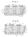
- FIG. 4 shows a conventional multilayer interconnection layer 4A without any power supply matching layer.
- the multilayer interconnection layer 4A has semiconductor chips 1 to 3, which are the same as those of FIG. 1, mounted on it for comparison with the present invention.
- FIG. 5 illustrates a conventional multilayer interconnection layer 4A in which the layout of semiconductor chips 1 to 3 is modified as in the embodiment of FIG. 2.
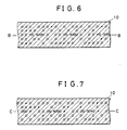
- FIGS. 6 and 7 show cross-sectional views taken along the lines B-B and the C-C in FIGS. 4 and 5, respectively.
- FIGS. 6 and 7 it will be noted by comparing FIGS. 6 and 7 that two multilayer interconnection substrates are different in position of each of noncontact through holes (hollow circle) and connected through holes (solid circle). Thus, it is necessary to design different conductor patterns for these multilayer interconnection substrates.
- the first and second embodiments of the present invention have the same pattern of the corresponding power supply layer 10 as shown in FIG. 3, and hence the corresponding power supply layers 10 have the same design pattern.
- each of the power supply layers, signal pins and power supply pins are standardized for the power supply system, including impedance matching system, of a variety of multilayer interconnection substrates.
- impedance matching system of a variety of multilayer interconnection substrates.
- the design of the power supply system of multilayer interconnection substrates is carried out in the common power supply layers, the component mounting layer, which corresponds to each component to be mounted, the enlarged layer and the power supply matching layers, and it is possible to design the power supply system other than the signal layers.
- the man-hours of the design and the production cost are further reduced.
- the design of the signal layers is performed in view of the position of each through hole fixed according to standardization of signal pins.
- each through hole is standardized in position as well as the power supply layers. This simplifies the processes of punching, inspection, etc, thereby considerably reducing the production cost.
- the manufacturing cost takes a large part of the price of the product.
- the reduction in manufacturing cost due to reduction in both design manday and in the number of masks fully absorbs a raise in cost due to the increase of power supply matching layers and provides a considerable profit.
- the multilayer interconnection substrates of the first and the second embodiments provide a printed wiring board to which they are mounted with an advantage of standardized wiring layout of I/O pins.
- FIG. 8 schematically illustrates a third embodiment of the present invention.
- power supply matching layers are provided to chip carriers.
- semiconductor chips 21, 22, and 23 are mounted on respective chip carriers 31, 32, and 33, which are in turn mounted on a multilayer interconnection substrate 40.
- the multilayer interconnection substrate 40 is provided with signal layers 9, power supply layers 10, and through holes 11 to 13 and is further provided with I/O pins 5 and 6.
- the multilayer interconnection substrate 40 has the same structure as the multilayer interconnection substrates of the first and the second embodiments except that the enlarged layer 7 and the power supply matching layers 8 are not provided. Also, in the third embodiment, through holes 11 and 13 are formed at the same positions in a similar manner for respective chip sites.
- the electrical connection between power supply matching layers 35 of the chip carriers 31 to 33 and power supply layers 10 of the multilayer interconnection substrate 40 is made by connecting through holes 38 of chip carriers 31 to 33 to through holes 41 of multilayer interconnection substrate 40 through power supply bumps 19. This connection is distinct from the connection in the first embodiment of FIG. 1.
- Each of the through holes 36, 37 and 38 constitutes a chip connecting terminal portion at one end thereof on the side of the semiconductor chip mounting surface and a substrate connecting terminal portion at the other end on the side of the opposite surface to be placed on the multilayer interconnection substrate 40.
- the opposite ends of each through hole 36, 37, 38 are connected to power supply bumps 18 and 19, respectively.
- Each of the chip carriers 31, 32 and 33 is provided on its one surface with power supply bumps 18 for corresponding one of the semiconductor chips 21, 22 and 23.
- the power supply bumps 18 are connected to the chip connecting terminal portions of corresponding through holes 36, 37 and 38.
- Connected to the other surface of each chip carrier 31, 32, 33 are power supply bumps 19 for the multilayer interconnection substrate 40.
- the power supply bumps 19 are connected to substrate connecting terminal portions of corresponding through holes 36, 37 and 38.
- the chip carriers 31, 32 and 33 are each provided with an enlarged layer 34 and power supply matching layers 35.
- the enlarged layer 34 and power supply matching layers 35 are each sandwiched between adjacent insulating layers 17A as in the first embodiment.
- Each of the enlarged layers 34 absorbs misalignment between corresponding power supply bumps 18 and 19 and connects them through a through hole 36.
- the power supply matching layers 35 are provided in a number to correspond to voltages of semiconductor chips to be mounted.
- the power supply matching layers 35 are connected to power supply bumps 18 through through holes 37 and to power supply bumps 19 through through holes 38.
- Several through holes 37 and 38 are provided to correspond to power supply bumps 18 and 19, respectively.
- the power supply matching layers 35 of the chip carrier 31, 32, and 33 meet changes in power supply condition due to a variety of semiconductor chips and modification of the layout as shown in FIG. 8.
- the power supply layers 10 the through holes 11 to 13 and the I/O pins 5 and 6 of the multilayer interconnection substrate 40.
- the signal layers 9 and the chip carriers 31 to 33 may be designed independently, and hence the third embodiment achieves reduction in both the manhour of design and the number of masks of the multilayer interconnection substrate and moreover facilitates production thereof.
- the time to develop the multilayer interconnection substrate and the cost of production thereof are reduced.
- enlarged layers 34 are provided to the chip carriers 31, 32, and 33, they may be omitted.
- FIG. 9 A fourth embodiment of the present invention is illustrated in FIG. 9, in which the multilayer interconnection substrate has semiconductor chips mounted on its opposite surfaces; the two principal planes of the multilayer interconnection substrate serve as semiconductor element component mounting planes.
- One end surface (the left side end surface) of the multilayer interconnection substrate serves as a connector fitting surface.
- signal layers 9 and power supply layers 10 are superposed.
- FIG. 9 there are four signal layers 9 and three power supply layers 10.
- Power supply matching layers 81 are laid as top layers and power supply matching layers 82 as bottom layers.
- the power supply matching layers 81 and 82 are superposed through insulating layers 17.
- the multilayer interconnection substrate 60 is provided on its opposite major surfaces with bumps 16 for connecting to semiconductor chips 51 to 56.
- the multilayer interconnection substrate 60 is further provided with through holes 11 for connection with signal layers 9 and with through holes 14 for connection with power supply matching layers 81 or 82.
- Through holes 61 are also formed in the multilayer interconnection substrate 60 to interconnect power supply matching layers 81 and 82.
- the multilayer interconnection substrate 60 is provided on its one end with leads (not shown) of the power supply matching layers 81 and 82, the signal layers 9 and the power supply layers 10 for connection to the connector 70.
- the leads are provided with connection pins and a fitting mechanism (both not shown). More than one connector 70 may be provided.
- the power supply matching layers must be increased as the semiconductor chips to be mounted to the multilayer interconnection substrate 60 increase. In this embodiment, this requirement is met by increasing the power supply matching layers 81 and 82 without any adverse effect on the power supply layers 10. That is, without modifying the conductor pattern and the through holes, a variety of semiconductor chips may be mounted on the multilayer interconnection substrate 60, and the multilayer interconnection substrate 60 which enables various layouts may be produced with reduced manhour of design.
- the fourth embodiment also provides the same advantages in ease of production and reduction of fabrication cost as the preceding embodiments.
- the number of the power supply matching layers may be changed to correspond to the design of the multilayer interconnection substrate on which semiconductor chips with a variety of voltages are mounted.
- the power supply layers which function as both impedance matching layers and power supply layers are increased. To do this, it is only necessary to determine additional connecting points of power supply layers to through holes, and thus, time and labor to redesign the multilayer interconnection substrate are eliminated.
- each of the power supply layers below or inside the power supply matching layers of the multilayer interconnection substrates has the same pattern even if different sorts of semiconductor chips are mounted with a different layout.
- I/O pins are standardized.
- the standardization of the power supply layers reduces the manhour of design of the multilayer interconnection substrate and the number of print masks to be prepared.
- the position of each of the through holes is also standardized.
- the standardization of the power supply layers and the positions of the through holes makes the process of fabrication of the multilayer interconnection substrate less complicated than the prior art, resulting in ease of fabrication of the multilayer interconnection substrate. Thus, the time of development of the product and cost of fabrication are reduced.
- One or some of the power supply layers may be applied with a voltage of ground throughout the embodiments of the present invention.
Applications Claiming Priority (2)
| Application Number | Priority Date | Filing Date | Title |
|---|---|---|---|
| JP214542/89 | 1989-08-21 | ||
| JP1214542A JPH0378290A (ja) | 1989-08-21 | 1989-08-21 | 多層配線基板 |
Publications (2)
| Publication Number | Publication Date |
|---|---|
| EP0414204A2 true EP0414204A2 (fr) | 1991-02-27 |
| EP0414204A3 EP0414204A3 (en) | 1991-05-08 |
Family
ID=16657465
Family Applications (1)
| Application Number | Title | Priority Date | Filing Date |
|---|---|---|---|
| EP19900115984 Withdrawn EP0414204A3 (en) | 1989-08-21 | 1990-08-21 | Multilayer interconnection substrate and semiconductor integrated circuit device using the same |
Country Status (3)
| Country | Link |
|---|---|
| EP (1) | EP0414204A3 (fr) |
| JP (1) | JPH0378290A (fr) |
| KR (1) | KR930001621B1 (fr) |
Cited By (9)
| Publication number | Priority date | Publication date | Assignee | Title |
|---|---|---|---|---|
| FR2675946A1 (fr) * | 1991-04-25 | 1992-10-30 | Sorep | Procede de montage d'une puce a circuit integre sur un substrat de cablage. |
| EP0582315A1 (fr) * | 1992-08-07 | 1994-02-09 | Fujitsu Limited | Substrats fonctionnels pour l'empaquetage de puces semi-conductrices |
| US5382827A (en) * | 1992-08-07 | 1995-01-17 | Fujitsu Limited | Functional substrates for packaging semiconductor chips |
| FR2715771A1 (fr) * | 1994-02-02 | 1995-08-04 | Matra Marconi Space France | Assemblage de microcircuits intégrés de type puce à protubérances. |
| US5543661A (en) * | 1994-05-31 | 1996-08-06 | Sumitomo Metal Ceramics Inc. | Semiconductor ceramic package with terminal vias |
| US5714801A (en) * | 1995-03-31 | 1998-02-03 | Kabushiki Kaisha Toshiba | Semiconductor package |
| US5777383A (en) * | 1996-05-09 | 1998-07-07 | Lsi Logic Corporation | Semiconductor chip package with interconnect layers and routing and testing methods |
| DE4325668C2 (de) * | 1992-07-30 | 1999-06-24 | Toshiba Kawasaki Kk | Mehrebenen-Verdrahtungssubstrat und dieses verwendende Halbleiteranordnung |
| US7057272B2 (en) * | 2002-06-26 | 2006-06-06 | Fujitsu Limited | Power supply connection structure to a semiconductor device |
Families Citing this family (1)
| Publication number | Priority date | Publication date | Assignee | Title |
|---|---|---|---|---|
| JP2002185141A (ja) * | 2000-12-15 | 2002-06-28 | Ibiden Co Ltd | 多層プリント配線板 |
Citations (5)
| Publication number | Priority date | Publication date | Assignee | Title |
|---|---|---|---|---|
| US4245273A (en) * | 1979-06-29 | 1981-01-13 | International Business Machines Corporation | Package for mounting and interconnecting a plurality of large scale integrated semiconductor devices |
| JPS5939057A (ja) * | 1982-08-27 | 1984-03-03 | Hitachi Ltd | 半導体記憶装置 |
| FR2563656A1 (fr) * | 1984-04-27 | 1985-10-31 | Nec Corp | Bloc de circuits a integration a grande echelle |
| EP0268111A2 (fr) * | 1986-11-17 | 1988-05-25 | International Business Machines Corporation | Procédé pour effectuer une modification technique des interconnexions entre plusieurs circuits intégrés en utilisant des pièces intermédiaires |
| EP0285064A2 (fr) * | 1987-04-01 | 1988-10-05 | Hitachi, Ltd. | Structure de module à plusieurs puces |
-
1989
- 1989-08-21 JP JP1214542A patent/JPH0378290A/ja active Pending
-
1990
- 1990-08-18 KR KR1019900012712A patent/KR930001621B1/ko not_active IP Right Cessation
- 1990-08-21 EP EP19900115984 patent/EP0414204A3/en not_active Withdrawn
Patent Citations (5)
| Publication number | Priority date | Publication date | Assignee | Title |
|---|---|---|---|---|
| US4245273A (en) * | 1979-06-29 | 1981-01-13 | International Business Machines Corporation | Package for mounting and interconnecting a plurality of large scale integrated semiconductor devices |
| JPS5939057A (ja) * | 1982-08-27 | 1984-03-03 | Hitachi Ltd | 半導体記憶装置 |
| FR2563656A1 (fr) * | 1984-04-27 | 1985-10-31 | Nec Corp | Bloc de circuits a integration a grande echelle |
| EP0268111A2 (fr) * | 1986-11-17 | 1988-05-25 | International Business Machines Corporation | Procédé pour effectuer une modification technique des interconnexions entre plusieurs circuits intégrés en utilisant des pièces intermédiaires |
| EP0285064A2 (fr) * | 1987-04-01 | 1988-10-05 | Hitachi, Ltd. | Structure de module à plusieurs puces |
Non-Patent Citations (4)
| Title |
|---|
| IBM TECHNICAL DISCLOSURE BULLETIN, vol. 13, no. 3, August 1970, page 622, New York, US; A.J. BLODGETT, Jr.: "Microelectronic ceramic substrate with improved voltage distribution" * |
| IBM TECHNICAL DISCLOSURE BULLETIN, vol. 22, no. 5, October 1979, pages 1841-1842, New York, US; A.H. JOHNSON et al.: "Multilayer ceramic fixed layer substrate design" * |
| IBM TECHNICAL DISCLOSURE BULLETIN, vol. 27, no. 4B, September 1984, pages 2348-2351, New York, US; E.M. HUBACHER: "Low cost multi-chip package" * |
| PATENT ABSTRACTS OF JAPAN, vol. 8, no. 127 (E-250)[1564], 14th June 1984; & JP-A-59 39 057 (HITACHI) 03-03-1984 * |
Cited By (11)
| Publication number | Priority date | Publication date | Assignee | Title |
|---|---|---|---|---|
| FR2675946A1 (fr) * | 1991-04-25 | 1992-10-30 | Sorep | Procede de montage d'une puce a circuit integre sur un substrat de cablage. |
| WO1992020101A1 (fr) * | 1991-04-25 | 1992-11-12 | Societe Rennaise D'electronique Professionnelle (S.O.R.E.P.) | Procede de montage d'une puce a circuit integre sur un substrat de cablage |
| DE4325668C2 (de) * | 1992-07-30 | 1999-06-24 | Toshiba Kawasaki Kk | Mehrebenen-Verdrahtungssubstrat und dieses verwendende Halbleiteranordnung |
| EP0582315A1 (fr) * | 1992-08-07 | 1994-02-09 | Fujitsu Limited | Substrats fonctionnels pour l'empaquetage de puces semi-conductrices |
| US5382827A (en) * | 1992-08-07 | 1995-01-17 | Fujitsu Limited | Functional substrates for packaging semiconductor chips |
| US5475262A (en) * | 1992-08-07 | 1995-12-12 | Fujitsu Limited | Functional substrates for packaging semiconductor chips |
| FR2715771A1 (fr) * | 1994-02-02 | 1995-08-04 | Matra Marconi Space France | Assemblage de microcircuits intégrés de type puce à protubérances. |
| US5543661A (en) * | 1994-05-31 | 1996-08-06 | Sumitomo Metal Ceramics Inc. | Semiconductor ceramic package with terminal vias |
| US5714801A (en) * | 1995-03-31 | 1998-02-03 | Kabushiki Kaisha Toshiba | Semiconductor package |
| US5777383A (en) * | 1996-05-09 | 1998-07-07 | Lsi Logic Corporation | Semiconductor chip package with interconnect layers and routing and testing methods |
| US7057272B2 (en) * | 2002-06-26 | 2006-06-06 | Fujitsu Limited | Power supply connection structure to a semiconductor device |
Also Published As
| Publication number | Publication date |
|---|---|
| JPH0378290A (ja) | 1991-04-03 |
| KR910005740A (ko) | 1991-03-30 |
| EP0414204A3 (en) | 1991-05-08 |
| KR930001621B1 (ko) | 1993-03-06 |
Similar Documents
| Publication | Publication Date | Title |
|---|---|---|
| US4249302A (en) | Multilayer printed circuit board | |
| CA1143862A (fr) | Semiconducteur haute performance | |
| US7530167B2 (en) | Method of making a printed circuit board with low cross-talk noise | |
| US5471090A (en) | Electronic structures having a joining geometry providing reduced capacitive loading | |
| US4202007A (en) | Multi-layer dielectric planar structure having an internal conductor pattern characterized with opposite terminations disposed at a common edge surface of the layers | |
| US5770476A (en) | Passive interposer including at least one passive electronic component | |
| EP0042987B1 (fr) | Substrat contenant un circuit électronique pour un élément semiconducteur | |
| US5110664A (en) | Thick film and thin film composite substrate and electronic circuit apparatus using it | |
| KR960006982B1 (ko) | 계단형 다층 상호 연결 장치 | |
| EP0400332B1 (fr) | Méthode de fabrication d'un assemblage d'interconnexion sur une plaque multicouche utilisant des pellicules minces | |
| JP2005515611A (ja) | インターポーザを有する高性能低コスト超小型回路パッケージ | |
| US6407343B1 (en) | Multilayer wiring board | |
| EP0629107A2 (fr) | Technique de panneaux à cristaux imprimés à câblage et coupe transversale multiple | |
| KR20020077214A (ko) | 반도체장치 및 그 제조방법 | |
| JPH07272932A (ja) | プリントインダクタ | |
| EP0414204A2 (fr) | Substrat d'interconnexion à multicouche et dispositif semi-conducteur à circuit intégré comprenant ce substrat | |
| US4193082A (en) | Multi-layer dielectric structure | |
| US4894708A (en) | LSI package having a multilayer ceramic substrate | |
| US6476695B1 (en) | High frequency module | |
| EP0797254B1 (fr) | Empaquetage pour LSI et procédé de fabrication | |
| US6351391B1 (en) | Signal busses on printed board structures mounting ASIC chips with signal termination resistor devices using planar signal terminating devices | |
| JP3408590B2 (ja) | 多層プリント基板の配線構造 | |
| JP2837521B2 (ja) | 半導体集積回路装置およびその配線変更方法 | |
| JPH01239964A (ja) | 半導体集積回路の電源配線レイアウト法 | |
| US6801439B2 (en) | Multiple network electronic component |
Legal Events
| Date | Code | Title | Description |
|---|---|---|---|
| PUAI | Public reference made under article 153(3) epc to a published international application that has entered the european phase |
Free format text: ORIGINAL CODE: 0009012 |
|
| 17P | Request for examination filed |
Effective date: 19900821 |
|
| AK | Designated contracting states |
Kind code of ref document: A2 Designated state(s): DE GB |
|
| PUAL | Search report despatched |
Free format text: ORIGINAL CODE: 0009013 |
|
| AK | Designated contracting states |
Kind code of ref document: A3 Designated state(s): DE GB |
|
| 17Q | First examination report despatched |
Effective date: 19930915 |
|
| STAA | Information on the status of an ep patent application or granted ep patent |
Free format text: STATUS: THE APPLICATION HAS BEEN WITHDRAWN |
|
| 18W | Application withdrawn |
Withdrawal date: 19940125 |