EP0409746B1 - Integrierter VDMOS/Logikschaltkreis mit vertikalem Transistor vom Verarmungstyp und einer Zenerdiode - Google Patents
Integrierter VDMOS/Logikschaltkreis mit vertikalem Transistor vom Verarmungstyp und einer Zenerdiode Download PDFInfo
- Publication number
- EP0409746B1 EP0409746B1 EP90420329A EP90420329A EP0409746B1 EP 0409746 B1 EP0409746 B1 EP 0409746B1 EP 90420329 A EP90420329 A EP 90420329A EP 90420329 A EP90420329 A EP 90420329A EP 0409746 B1 EP0409746 B1 EP 0409746B1
- Authority
- EP
- European Patent Office
- Prior art keywords
- transistor
- depleted
- doping step
- vdmos
- type
- Prior art date
- Legal status (The legal status is an assumption and is not a legal conclusion. Google has not performed a legal analysis and makes no representation as to the accuracy of the status listed.)
- Expired - Lifetime
Links
- 238000001465 metallisation Methods 0.000 claims description 19
- 238000000034 method Methods 0.000 claims description 7
- 238000004519 manufacturing process Methods 0.000 claims description 6
- 239000000758 substrate Substances 0.000 claims description 5
- XUIMIQQOPSSXEZ-UHFFFAOYSA-N Silicon Chemical compound [Si] XUIMIQQOPSSXEZ-UHFFFAOYSA-N 0.000 claims description 3
- 229910052710 silicon Inorganic materials 0.000 claims description 3
- 239000010703 silicon Substances 0.000 claims description 3
- 238000005530 etching Methods 0.000 claims description 2
- 108091006146 Channels Proteins 0.000 claims 2
- 102000004129 N-Type Calcium Channels Human genes 0.000 claims 1
- 108090000699 N-Type Calcium Channels Proteins 0.000 claims 1
- 125000004429 atom Chemical group 0.000 description 10
- 230000000903 blocking effect Effects 0.000 description 3
- 238000009792 diffusion process Methods 0.000 description 3
- 230000015572 biosynthetic process Effects 0.000 description 2
- 230000003647 oxidation Effects 0.000 description 2
- 238000007254 oxidation reaction Methods 0.000 description 2
- 238000000429 assembly Methods 0.000 description 1
- 230000000712 assembly Effects 0.000 description 1
- 239000003990 capacitor Substances 0.000 description 1
- 238000000151 deposition Methods 0.000 description 1
- 230000008021 deposition Effects 0.000 description 1
- 238000000407 epitaxy Methods 0.000 description 1
- 230000010354 integration Effects 0.000 description 1
- 230000000873 masking effect Effects 0.000 description 1
- 229910021420 polycrystalline silicon Inorganic materials 0.000 description 1
- 238000010405 reoxidation reaction Methods 0.000 description 1
Images

Classifications
-
- H—ELECTRICITY
- H01—ELECTRIC ELEMENTS
- H01L—SEMICONDUCTOR DEVICES NOT COVERED BY CLASS H10
- H01L29/00—Semiconductor devices specially adapted for rectifying, amplifying, oscillating or switching and having potential barriers; Capacitors or resistors having potential barriers, e.g. a PN-junction depletion layer or carrier concentration layer; Details of semiconductor bodies or of electrodes thereof ; Multistep manufacturing processes therefor
- H01L29/66—Types of semiconductor device ; Multistep manufacturing processes therefor
- H01L29/68—Types of semiconductor device ; Multistep manufacturing processes therefor controllable by only the electric current supplied, or only the electric potential applied, to an electrode which does not carry the current to be rectified, amplified or switched
- H01L29/76—Unipolar devices, e.g. field effect transistors
- H01L29/772—Field effect transistors
- H01L29/78—Field effect transistors with field effect produced by an insulated gate
- H01L29/7827—Vertical transistors
- H01L29/7828—Vertical transistors without inversion channel, e.g. vertical ACCUFETs, normally-on vertical MISFETs
-
- H—ELECTRICITY
- H01—ELECTRIC ELEMENTS
- H01L—SEMICONDUCTOR DEVICES NOT COVERED BY CLASS H10
- H01L27/00—Devices consisting of a plurality of semiconductor or other solid-state components formed in or on a common substrate
- H01L27/02—Devices consisting of a plurality of semiconductor or other solid-state components formed in or on a common substrate including semiconductor components specially adapted for rectifying, oscillating, amplifying or switching and having potential barriers; including integrated passive circuit elements having potential barriers
- H01L27/04—Devices consisting of a plurality of semiconductor or other solid-state components formed in or on a common substrate including semiconductor components specially adapted for rectifying, oscillating, amplifying or switching and having potential barriers; including integrated passive circuit elements having potential barriers the substrate being a semiconductor body
- H01L27/08—Devices consisting of a plurality of semiconductor or other solid-state components formed in or on a common substrate including semiconductor components specially adapted for rectifying, oscillating, amplifying or switching and having potential barriers; including integrated passive circuit elements having potential barriers the substrate being a semiconductor body including only semiconductor components of a single kind
-
- H—ELECTRICITY
- H01—ELECTRIC ELEMENTS
- H01L—SEMICONDUCTOR DEVICES NOT COVERED BY CLASS H10
- H01L27/00—Devices consisting of a plurality of semiconductor or other solid-state components formed in or on a common substrate
- H01L27/02—Devices consisting of a plurality of semiconductor or other solid-state components formed in or on a common substrate including semiconductor components specially adapted for rectifying, oscillating, amplifying or switching and having potential barriers; including integrated passive circuit elements having potential barriers
- H01L27/0203—Particular design considerations for integrated circuits
- H01L27/0214—Particular design considerations for integrated circuits for internal polarisation, e.g. I2L
- H01L27/0218—Particular design considerations for integrated circuits for internal polarisation, e.g. I2L of field effect structures
-
- H—ELECTRICITY
- H01—ELECTRIC ELEMENTS
- H01L—SEMICONDUCTOR DEVICES NOT COVERED BY CLASS H10
- H01L27/00—Devices consisting of a plurality of semiconductor or other solid-state components formed in or on a common substrate
- H01L27/02—Devices consisting of a plurality of semiconductor or other solid-state components formed in or on a common substrate including semiconductor components specially adapted for rectifying, oscillating, amplifying or switching and having potential barriers; including integrated passive circuit elements having potential barriers
- H01L27/04—Devices consisting of a plurality of semiconductor or other solid-state components formed in or on a common substrate including semiconductor components specially adapted for rectifying, oscillating, amplifying or switching and having potential barriers; including integrated passive circuit elements having potential barriers the substrate being a semiconductor body
- H01L27/06—Devices consisting of a plurality of semiconductor or other solid-state components formed in or on a common substrate including semiconductor components specially adapted for rectifying, oscillating, amplifying or switching and having potential barriers; including integrated passive circuit elements having potential barriers the substrate being a semiconductor body including a plurality of individual components in a non-repetitive configuration
- H01L27/0611—Devices consisting of a plurality of semiconductor or other solid-state components formed in or on a common substrate including semiconductor components specially adapted for rectifying, oscillating, amplifying or switching and having potential barriers; including integrated passive circuit elements having potential barriers the substrate being a semiconductor body including a plurality of individual components in a non-repetitive configuration integrated circuits having a two-dimensional layout of components without a common active region
- H01L27/0617—Devices consisting of a plurality of semiconductor or other solid-state components formed in or on a common substrate including semiconductor components specially adapted for rectifying, oscillating, amplifying or switching and having potential barriers; including integrated passive circuit elements having potential barriers the substrate being a semiconductor body including a plurality of individual components in a non-repetitive configuration integrated circuits having a two-dimensional layout of components without a common active region comprising components of the field-effect type
- H01L27/0629—Devices consisting of a plurality of semiconductor or other solid-state components formed in or on a common substrate including semiconductor components specially adapted for rectifying, oscillating, amplifying or switching and having potential barriers; including integrated passive circuit elements having potential barriers the substrate being a semiconductor body including a plurality of individual components in a non-repetitive configuration integrated circuits having a two-dimensional layout of components without a common active region comprising components of the field-effect type in combination with diodes, or resistors, or capacitors
-
- H—ELECTRICITY
- H01—ELECTRIC ELEMENTS
- H01L—SEMICONDUCTOR DEVICES NOT COVERED BY CLASS H10
- H01L27/00—Devices consisting of a plurality of semiconductor or other solid-state components formed in or on a common substrate
- H01L27/02—Devices consisting of a plurality of semiconductor or other solid-state components formed in or on a common substrate including semiconductor components specially adapted for rectifying, oscillating, amplifying or switching and having potential barriers; including integrated passive circuit elements having potential barriers
- H01L27/04—Devices consisting of a plurality of semiconductor or other solid-state components formed in or on a common substrate including semiconductor components specially adapted for rectifying, oscillating, amplifying or switching and having potential barriers; including integrated passive circuit elements having potential barriers the substrate being a semiconductor body
- H01L27/08—Devices consisting of a plurality of semiconductor or other solid-state components formed in or on a common substrate including semiconductor components specially adapted for rectifying, oscillating, amplifying or switching and having potential barriers; including integrated passive circuit elements having potential barriers the substrate being a semiconductor body including only semiconductor components of a single kind
- H01L27/085—Devices consisting of a plurality of semiconductor or other solid-state components formed in or on a common substrate including semiconductor components specially adapted for rectifying, oscillating, amplifying or switching and having potential barriers; including integrated passive circuit elements having potential barriers the substrate being a semiconductor body including only semiconductor components of a single kind including field-effect components only
- H01L27/088—Devices consisting of a plurality of semiconductor or other solid-state components formed in or on a common substrate including semiconductor components specially adapted for rectifying, oscillating, amplifying or switching and having potential barriers; including integrated passive circuit elements having potential barriers the substrate being a semiconductor body including only semiconductor components of a single kind including field-effect components only the components being field-effect transistors with insulated gate
- H01L27/0883—Combination of depletion and enhancement field effect transistors
-
- H—ELECTRICITY
- H01—ELECTRIC ELEMENTS
- H01L—SEMICONDUCTOR DEVICES NOT COVERED BY CLASS H10
- H01L29/00—Semiconductor devices specially adapted for rectifying, amplifying, oscillating or switching and having potential barriers; Capacitors or resistors having potential barriers, e.g. a PN-junction depletion layer or carrier concentration layer; Details of semiconductor bodies or of electrodes thereof ; Multistep manufacturing processes therefor
- H01L29/66—Types of semiconductor device ; Multistep manufacturing processes therefor
- H01L29/68—Types of semiconductor device ; Multistep manufacturing processes therefor controllable by only the electric current supplied, or only the electric potential applied, to an electrode which does not carry the current to be rectified, amplified or switched
- H01L29/76—Unipolar devices, e.g. field effect transistors
- H01L29/772—Field effect transistors
- H01L29/78—Field effect transistors with field effect produced by an insulated gate
- H01L29/7801—DMOS transistors, i.e. MISFETs with a channel accommodating body or base region adjoining a drain drift region
- H01L29/7802—Vertical DMOS transistors, i.e. VDMOS transistors
Definitions
- the present invention relates to the field of integrated power circuits including a logic part on the same chip. It relates more particularly to structures of the VDMOS transistor type in which logic circuits with N channel MOS transistors of the lateral type enriched and depleted are also produced.
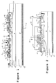
- Figure 1 is a highly schematic sectional view of such a structure. Only certain elements of this structure are represented for the sake of simplification (in particular certain layers of thin and thick oxide are not shown).
- the right part of the figure illustrates a power structure 1 of the VDMOS transistor type (vertical MOS transistor with diffused channel) with enrichment and the left part of the figure represents logic components such as a lateral N channel MOS transistor depleted 2 and an enriched N-channel lateral MOS transistor 3.
- VDMOS transistor type vertical MOS transistor with diffused channel
- logic components such as a lateral N channel MOS transistor depleted 2 and an enriched N-channel lateral MOS transistor 3.
- This structure is produced on a substrate comprising a layer N of type N formed by epitaxy on a silicon wafer 11 of type N + .
- P-type regions 12 are formed, corresponding in particular to wells in which the logic part of the chip will be developed.
- P + regions are formed with a high doping level, high enough to obtain ohmic contact with metallizations. These regions P + are for example regions 17 making it possible to make an ohmic contact with the well 12 and regions 18 of the power transistor making it possible to make contact with the so-called "bulk" region in a surface part of which the channel.
- N-type regions 13 are formed, corresponding in particular to the channel regions of the depleted lateral MOS transistors.
- the gates 21 of the enriched VDMOS transistor, 22 of the enriched lateral MOS transistors, and 23 of the depleted lateral MOS transistors are formed simultaneously .
- a fourth P-type doping step in the region of the vertical power transistor cells is used to form the channel regions 30 of these transistors, the gate regions serving as a mask.
- N + regions are formed, again using in particular the above-mentioned gates as a mask, corresponding in particular to the sources 32 of the power transistor 1 and to the sources and drains 33 to 36 of the depleted lateral MOS transistors. and enriched 2 and 3.
- a metallization layer is formed in which the source metallization 41 of the power transistor is cut, and the source and drain metallizations 42 to 45 of the lateral transistors as well as other metallizations such as contact metallizations 46 of the boxes in which the logic components are formed.
- such a structure In operation, such a structure is generally connected so that its rear face 48 is at the most positive potential (+ V HT ), all the other metallizations (except in certain assemblies the gate metallization of the power transistor) being at potentials lower and the metallization 46 of the box 12 being commonly connected to ground.
- the structure described above is particularly attractive by its simplicity. Indeed, it requires a minimum number of masking and doping steps. As we saw previously, only five types of doping are planned.
- this prior patent proposes to reduce the high voltage appearing on the underside of the component to the upper face by means of an N + diffusion and then to distribute this high voltage by a spiral resistance.
- an object of the present invention is to provide, in an integrated circuit produced according to the technology described above, and without increasing the number of manufacturing steps, means for bringing the high voltage available on the lower face to the upper face. .
- Another object of the present invention is to provide a reference voltage from the high voltage available on the underside.
- Another object of the present invention is to allow such a reference voltage to be obtained without causing significant consumption of the integrated circuit.
- the present invention first of all provides in a structure of the type described above, an additional component, namely a depleted vertical MOS transistor.
- a method of manufacturing an integrated circuit according to the invention is defined by the terms of claim 1.
- a circuit according to the invention is defined by the terms of claim 5.
- the present invention provides for forming a zener diode comprising an N + region resulting from the fifth doping step formed in a P region resulting from the fourth doping step.
- a zener diode is obtained whose triggering voltage is close to the threshold voltage of the depleted MOS transistor.
- this transistor operates in the vicinity of its blocking zone and is therefore relatively resistive, which limits the current consumption of the circuit.
- FIG. 2 represents a partial section view of a component according to the present invention formed in a structure of the type of that of FIG. 1. This figure represents more particularly in its left part a depleted VDMOS transistor (vertical MOS transistor) 60 and in its right part a zener diode 70.
- VDMOS transistor vertical MOS transistor
- the depleted VDMOS transistor is produced by forming its P-type well 61 - during the first doping step, at the same time as the well 12 of the logic circuits is formed.
- the third doping step while forming the N - channel layer of the depleted logic transistors, we simultaneously form an N - 62 layer which will correspond to the depleted channel region of the transistor 60.
- we form conventionally an isolated grid 63 this isolated grid 63 is represented as off-center with respect to box 61, in fact, there are no self-alignment steps between the formation of the box and the formation of the grid, but this is of no practical importance since the channel is formed in the region 62 and not in region 61).
- N + type source diffusions 64 are produced during the fifth doping step.
- P + type regions 65 produced during the second doping step make it possible to make contacts with the well.
- Reference 66 designates a source metallization and reference 67 designates a bulk metallization. It will be noted that these metallizations are optionally separated by a thick oxide zone 68. The drain of this depleted VDMOS transistor is common with that of the enriched VDMOS transistor 1 and corresponds to metallization 48.
- the right part of the figure represents a zener diode obtained by a P-type diffusion 71 resulting from the fourth doping step in which an N + type region 72 resulting from the fifth doping step is formed.
- the P type region 71 has a doping level which corresponds to that of the wells 30 of the enriched VDMOS transistor of FIG. 1.
- This diode is conventionally surrounded by a ring 73 of P + type corresponding to the second doping step and on which an anode metallization 74 is formed, a cathode metallization 75 being formed on the N + region 72.
- the present invention makes it possible to form a depleted VDMOS transistor and a zener diode without adding a single step to the conventional technological process for manufacturing a structure with an enriched VDMOS power transistor and with logic transistors of the enriched and depleted lateral MOS type.
- Figures 3 and 4 show the two usual modes of mounting a load L in series with a switch consisting of an enriched VDMOS transistor with N channel.
- FIG. 3 represents a circuit conventionally designated by the name "high side”, that is to say a circuit in which a load L is connected to ground and the drain of the VDMOS transistor 1 at high voltage.
- FIG. 4 represents a so-called “low side” arrangement in which the load L is connected to the high voltage and the source of the VDMOS transistor 1 to ground.
- VT threshold voltage
- the present invention proposes to achieve this result by performing an assembly of the type illustrated in FIG. 5.
- FIG. 5 represents a depleted VDMOS transistor 60 connected to a zener diode 70.
- the anode of the zener diode is connected to the gate and to the box of the depleted VDMOS transistor and the cathode of the zener diode is connected to the source of the depleted transistor , the drain of the depleted transistor 60 being connected to the drain of the main enriched VDMOS transistor 1.
- connection mode is also illustrated in FIG. 2, the connection between the gate and the substrate of the transistor 60 being designated by the reference 82, the connection between the well of the depleted VDMOS transistor and the anode of the zener diode 70 being made by metallization 67-74, and the connection between the cathode of the zener diode and the source of the depleted VDMOS transistor being designated by the reference 84.
- VZ which can be applied by a switch 90 (produced by a logic circuit of enriched and depleted lateral MOS transistors formed on the same chip) towards the gate of the transistor.
- the anode of the zener diode is also connected to a reference voltage VR which may either be the source of the enriched VDMOS transistor or else ground or another chosen voltage lower than VD.
- a Darlington pair of bipolar transistors may be added to this arrangement, the base of the Darlington being connected to the source of the depleted VDMOS transistor 60, the Darlington collector being connected to the drains of the VDMOS transistors, and the Darlington transmitter being connected to the terminal of the switch 90 opposite the grid of the enriched VDMOS 1.
- the enriched VDMOS transistor being initially blocked, the closing of the switch 90 makes it possible to apply the voltage of 10 volts chosen on the grid.
- the enriched VDMOS transistor becomes conductive, the potential of its source, VS, becomes substantially equal to that of its drain, VD, and it will conventionally be necessary to add to the circuit of FIG. 5 a charge pump circuit for provide a higher voltage than VD of about 10 volts.
- a voltage is available on the drain of the enriched VDMOS transistor when the latter is in the blocked state.
- the transistor 1 when the transistor 1 is conductive, the voltage drop across its terminals becomes less than VZ and there is therefore no more voltage available at the switch 90.
- the circuit according to the present invention may nevertheless be used with a capacitor in parallel on the zener diode 70 to maintain the control voltage during the conduction phases of the enriched VDMOS transistor in the usual case where the power transistor is controlled by switching with brief successive periods of conduction and blocking.
- the P-type region 71 of the anode of the zener diode may be formed in an extension of the region 61 corresponding to the well of the depleted transistor 60.
Landscapes
- Engineering & Computer Science (AREA)
- Power Engineering (AREA)
- Microelectronics & Electronic Packaging (AREA)
- Physics & Mathematics (AREA)
- Condensed Matter Physics & Semiconductors (AREA)
- General Physics & Mathematics (AREA)
- Computer Hardware Design (AREA)
- Ceramic Engineering (AREA)
- Metal-Oxide And Bipolar Metal-Oxide Semiconductor Integrated Circuits (AREA)
Claims (5)
- Verfahren zum Herstellen eines integrierten Schaltkreises mit Leistungskomponenten aus MOS-Vertikaltransistoren (VDMOS) vom Anreicherungstyp (1) und Logikkomponenten aus MOS-Flächentransistoren vom Verarmungstyp (2) und Anreicherungstyp (3), in einem Epitaxiesubstrat vom Typ N/N+ (10, 11) mit folgenden Schritten:einem ersten P-Typ-Dotierungsschritt, um Zonen entsprechend einem Graben (12) zu bilden, in dem die logischen Transistoren ausgebildet werden,einem zweiten P-Typ-Dotierungsschritt mit erhöhter Dotierung, der die Einrichtung von ohmschen Kontakten (17, 18) erlaubt,einem dritten N-Typ-Dotierungsschritt, um die Kanalzonen (13) der MOS-Transistoren vom Verarmungstyp auszubilden,einem vierten P-Typ-Dotierungsschritt, um Zonen (30) entsprechend Kanalzonen des VDMOS-Transistor auszubilden,einem fünften N-Typ-Dotierungsschritt mit erhöhter Dotierung, der die Ausbildung von ohmschen Kontakten (32 - 36) erlaubt,einem einzelnen Metallisierungsschritt, um durch Ätzen verschiedene metallisierte Bereiche auf der Oberfläche auszubilden,dadurch gekennzeichnet, daß das Verfahren darüberhinaus die Herstellung eines VDMOS-Transistors mit einem N-Kanal vom Verarmungstyp (60) mit einer mit dem VDMOS-Transistor vom Anreicherungstyp (1) gemeinsamen Drain umfaßt, der einen Bereich eines N-Kanales (62) aufweist, der aus dem dritten Dotierungsschritt resultiert , einen P-Graben (61), der aus dem ersten Dotierungsschritt resultiert und Bereiche einer N+-Source (64), die in den genannten Gräben ausgebildet werden und aus dem fünften Dotierungsschritt resultiert.
- Verfahren nach Anspruch 1, dadurch gekennzeichnet, daß es darüberhinaus die Herstellung einer Zenerdiode (70) umfaßt, die einen N+-Bereich (72) aufweist, der aus dem fünften Dotierungsschritt resultiert und in einem P-Bereich (71) gebildet wird, der aus dem vierten Dotierungsschritt resultiert.
- Verfahren nach Anspruch 2, dadurch gekennzeichnet, daß der P-Bereich der Zenerdiode in der N-Epitaxieschicht des Substrates ausgebildet wird.
- Verfahren nach Anspruch 2, dadurch gekennzeichnet, daß der P-Bereich der Zenerdiode in einem Bereich ausgebildet wird, der aus dem zweiten Dotierungsschritt resultiert und verlängert wird, um einen Graben des VDMOS-Transistors vom Verarmungstyp auszubilden.
- Integrierter Schaltkreis mit Leistungskomponenten aus MOS-Vertikaltransistoren (VDMOS) vom Anreicherungstyp (1), die in einer Epitaxiescheibe aus N/N+-Silicium ausgebildet sind, und mit Logikkomponenten aus MOS-Flächentransistoren vom Verarmungstyp (2) und Anreicherungstyp (3), die in einem P-Graben der Epitaxieschicht ausgebildet sind, dadurch gekennzeichnet, daß er darüberhinaus eine interne Referenzspannung aufweist, die aus einer Serienschaltung eines VDMOS-Transistors vom Verarmungstyp (60) mit einer mit dem VDMOS-Transistor vom Anreicherungstyp gemeinsamen Drain und einer Zenerdiode (70) ausgebildet ist, die in einem P-Graben der Epitaxieschicht ausgebildet ist, deren Kathode mit der Source des VDMOS-Transistors vom Verarmungstyp verbunden ist und deren Anode mit dem Substrat und dem Gate dieses VDMOS-Transistors vom Verarmungstyp verbunden ist.
Applications Claiming Priority (2)
| Application Number | Priority Date | Filing Date | Title |
|---|---|---|---|
| FR8909911 | 1989-07-17 | ||
| FR8909911A FR2649828B1 (fr) | 1989-07-17 | 1989-07-17 | Circuit integre vdmos/logique comprenant un transistor vertical deplete et une diode zener |
Publications (2)
| Publication Number | Publication Date |
|---|---|
| EP0409746A1 EP0409746A1 (de) | 1991-01-23 |
| EP0409746B1 true EP0409746B1 (de) | 1997-05-28 |
Family
ID=9384056
Family Applications (1)
| Application Number | Title | Priority Date | Filing Date |
|---|---|---|---|
| EP90420329A Expired - Lifetime EP0409746B1 (de) | 1989-07-17 | 1990-07-11 | Integrierter VDMOS/Logikschaltkreis mit vertikalem Transistor vom Verarmungstyp und einer Zenerdiode |
Country Status (6)
| Country | Link |
|---|---|
| US (1) | US5045902A (de) |
| EP (1) | EP0409746B1 (de) |
| JP (1) | JPH0357267A (de) |
| KR (1) | KR910003807A (de) |
| DE (1) | DE69030791T2 (de) |
| FR (1) | FR2649828B1 (de) |
Families Citing this family (32)
| Publication number | Priority date | Publication date | Assignee | Title |
|---|---|---|---|---|
| US5223732A (en) * | 1991-05-28 | 1993-06-29 | Motorola, Inc. | Insulated gate semiconductor device with reduced based-to-source electrode short |
| JP3111576B2 (ja) * | 1992-01-06 | 2000-11-27 | 富士電機株式会社 | 半導体装置 |
| US5242841A (en) * | 1992-03-25 | 1993-09-07 | Texas Instruments Incorporated | Method of making LDMOS transistor with self-aligned source/backgate and photo-aligned gate |
| FR2698486B1 (fr) * | 1992-11-24 | 1995-03-10 | Sgs Thomson Microelectronics | Structure de protection contre les surtensions directes pour composant semiconducteur vertical. |
| EP0621636B1 (de) * | 1993-04-21 | 1999-07-14 | Consorzio per la Ricerca sulla Microelettronica nel Mezzogiorno | Integrierte Schutzschaltungsstruktur zum Schutz von logischen MOS-Leistungshalbleitenbauelementen von elektrostatischen Entladungen |
| JP3216743B2 (ja) * | 1993-04-22 | 2001-10-09 | 富士電機株式会社 | トランジスタ用保護ダイオード |
| EP0646964B1 (de) * | 1993-09-30 | 1999-12-15 | Consorzio per la Ricerca sulla Microelettronica nel Mezzogiorno | Integrierte aktive Klammerungsstruktur für den Schutz von Leistungsanordnungen gegen Überspannungen, und Verfahren zu ihrer Herstellung |
| JP3183020B2 (ja) * | 1994-03-17 | 2001-07-03 | 株式会社日立製作所 | 保護回路を内蔵した絶縁ゲート型半導体装置 |
| FR2725307B1 (fr) * | 1994-09-30 | 1996-12-20 | Sgs Thomson Microelectronics | Composant semiconducteur d'alimentation, de recirculation et de demagnetisation d'une charge selfique |
| EP0746042B1 (de) * | 1995-06-02 | 2004-03-31 | SILICONIX Incorporated | Bidirektional sperrender Graben-Leistungs-MOSFET |
| EP0765025A3 (de) * | 1995-09-21 | 1998-12-30 | Siemens Aktiengesellschaft | Anlaufschaltung und Halbleiterkörper für eine solche Anlaufschaltung |
| US5629536A (en) * | 1995-11-21 | 1997-05-13 | Motorola, Inc. | High voltage current limiter and method for making |
| US5578841A (en) * | 1995-12-18 | 1996-11-26 | Motorola, Inc. | Vertical MOSFET device having frontside and backside contacts |
| JP3917211B2 (ja) * | 1996-04-15 | 2007-05-23 | 三菱電機株式会社 | 半導体装置 |
| FR2751489B1 (fr) * | 1996-07-16 | 1998-10-16 | Sgs Thomson Microelectronics | Microdisjoncteur statique autoblocable |
| US6096608A (en) * | 1997-06-30 | 2000-08-01 | Siliconix Incorporated | Bidirectional trench gated power mosfet with submerged body bus extending underneath gate trench |
| US5911104A (en) * | 1998-02-20 | 1999-06-08 | Texas Instruments Incorporated | Integrated circuit combining high frequency bipolar and high power CMOS transistors |
| US6133591A (en) * | 1998-07-24 | 2000-10-17 | Philips Electronics North America Corporation | Silicon-on-insulator (SOI) hybrid transistor device structure |
| DE19935100B4 (de) * | 1999-07-27 | 2004-10-28 | Infineon Technologies Ag | Halbbrückenkonfiguration |
| CN100339946C (zh) * | 2004-12-22 | 2007-09-26 | 中国电子科技集团公司第二十四研究所 | 小比导通电阻的集成化大电流功率器件结构的设计方法 |
| DE102005046406B4 (de) * | 2005-09-28 | 2010-02-25 | Infineon Technologies Ag | Halbleiteranordnung mit einem elektrischen Verbraucher und einer Halbleitereinrichtung zur Steuerung der Stärke eines elektrischen Stroms |
| US7479444B2 (en) * | 2006-06-01 | 2009-01-20 | Micrel, Inc. | Method for forming Schottky diodes and ohmic contacts in the same integrated circuit |
| CN100466228C (zh) * | 2007-09-13 | 2009-03-04 | 无锡市晶源微电子有限公司 | 增强型和耗尽型垂直双扩散型场效应管单片集成制作工艺 |
| US7638857B2 (en) * | 2008-05-07 | 2009-12-29 | United Microelectronics Corp. | Structure of silicon controlled rectifier |
| CN102779759A (zh) * | 2012-07-31 | 2012-11-14 | 杭州士兰集成电路有限公司 | 耗尽型mosfet的制造方法 |
| CN102760754B (zh) * | 2012-07-31 | 2015-07-15 | 杭州士兰集成电路有限公司 | 耗尽型vdmos及其制造方法 |
| US9548294B2 (en) * | 2012-08-09 | 2017-01-17 | Fuji Electric Co., Ltd. | Semiconductor device with temperature-detecting diode |
| CN105529262A (zh) * | 2014-09-29 | 2016-04-27 | 无锡华润华晶微电子有限公司 | 一种垂直双扩散金属氧化物半导体场效应管及其制作方法 |
| CN104538395B (zh) * | 2015-01-08 | 2019-01-25 | 电子科技大学 | 一种功率vdmos器件二极管并联式esd防护机构 |
| CN104505390B (zh) * | 2015-01-08 | 2019-03-15 | 电子科技大学 | 集成式二极管链功率mos防静电保护结构 |
| US11437506B2 (en) * | 2017-11-13 | 2022-09-06 | Shindengen Electric Manufacturing Co., Ltd. | Wide-gap semiconductor device |
| TWI688192B (zh) * | 2018-11-06 | 2020-03-11 | 新唐科技股份有限公司 | 控制電路及其包含之半導體結構 |
Family Cites Families (8)
| Publication number | Priority date | Publication date | Assignee | Title |
|---|---|---|---|---|
| US4163988A (en) * | 1978-01-30 | 1979-08-07 | Xerox Corporation | Split gate V groove FET |
| DE3108726A1 (de) * | 1981-03-07 | 1982-09-16 | Deutsche Itt Industries Gmbh, 7800 Freiburg | Monolithisch integrierte referenzspannungsquelle |
| JPS5944862A (ja) * | 1982-09-07 | 1984-03-13 | Toshiba Corp | 半導体装置 |
| JPS61182264A (ja) * | 1985-02-08 | 1986-08-14 | Nissan Motor Co Ltd | 縦型mosトランジスタ |
| FR2596922B1 (fr) * | 1986-04-04 | 1988-05-20 | Thomson Csf | Resistance integree sur un substrat semi-conducteur |
| JPH0685441B2 (ja) * | 1986-06-18 | 1994-10-26 | 日産自動車株式会社 | 半導体装置 |
| GB2206993A (en) * | 1987-06-08 | 1989-01-18 | Philips Electronic Associated | A method of manufacturing a semiconductor device |
| JPH01147854A (ja) * | 1987-12-04 | 1989-06-09 | Nissan Motor Co Ltd | 半導体装置 |
-
1989
- 1989-07-17 FR FR8909911A patent/FR2649828B1/fr not_active Expired - Lifetime
-
1990
- 1990-07-11 DE DE69030791T patent/DE69030791T2/de not_active Expired - Fee Related
- 1990-07-11 EP EP90420329A patent/EP0409746B1/de not_active Expired - Lifetime
- 1990-07-14 KR KR1019900010728A patent/KR910003807A/ko not_active Application Discontinuation
- 1990-07-16 US US07/552,627 patent/US5045902A/en not_active Expired - Lifetime
- 1990-07-17 JP JP2187330A patent/JPH0357267A/ja active Pending
Also Published As
| Publication number | Publication date |
|---|---|
| JPH0357267A (ja) | 1991-03-12 |
| FR2649828A1 (fr) | 1991-01-18 |
| EP0409746A1 (de) | 1991-01-23 |
| US5045902A (en) | 1991-09-03 |
| DE69030791D1 (de) | 1997-07-03 |
| KR910003807A (ko) | 1991-02-28 |
| FR2649828B1 (fr) | 1991-10-31 |
| DE69030791T2 (de) | 1998-01-08 |
Similar Documents
| Publication | Publication Date | Title |
|---|---|---|
| EP0409746B1 (de) | Integrierter VDMOS/Logikschaltkreis mit vertikalem Transistor vom Verarmungstyp und einer Zenerdiode | |
| EP0357528B1 (de) | MOS-Transistor und Anwendung bei einer Freilaufdiode | |
| EP0388329B1 (de) | Steuerschaltung für einen MOS-Leistungstransistor mit induktiver Last | |
| FR2558010A1 (fr) | Procede pour la fabrication de transistors mos complementaires a basses tensions de seuil dans des circuits integres a haute densite et structure resultant de ce procede | |
| EP0543742A1 (de) | Monolithische Niederspannungsschutzdiode mit geringer Kapazität | |
| EP0432058B1 (de) | Dynamische Isolierschaltung für integrierte Schaltungen | |
| EP0599745A1 (de) | Überspannungsschutzstruktur für vertikale Halbleiterkomponenten | |
| FR2461360A1 (fr) | Procede de fabrication d'un transistor a effet de champ du type dmos a fonctionnement vertical et transistor obtenu par ce procede | |
| EP0328465A1 (de) | Gate-Steuerschaltung eines MOS-Leistungstransistors im Schaltbetrieb | |
| EP0359680B1 (de) | Integrierbare, aktive Diode | |
| EP0565435A1 (de) | Halbleiterbauteil mit komplementären Transistoren | |
| FR2776832A1 (fr) | Procede de fabrication de transistors jfet | |
| EP0581625A1 (de) | Multifunktionale elektronische Vorrichtung, insbesondere Element mit dynamischem, negativem Widerstandsverhalten und Zugehöriges Herstellungsverfahren | |
| EP0410911B1 (de) | Prozess zur Herstellung eines integrierten Leistungstransistor/Logik-Schaltkreises mit einer Diode. | |
| FR2496342A1 (fr) | Dispositif semi-conducteur du type metal-oxyde-semi-conducteur et son procede de fabrication | |
| EP0599739B1 (de) | Thyristor und Aufbau von Thyristoren mit gemeinsamer Katode | |
| FR2797525A1 (fr) | Commutateur bidirectionnel a performances en commutation ameliorees | |
| EP0704903B1 (de) | Halbleitervorrichtung zur Speisung, Rückleitung und Entmagnetisierung einer induktiven Last | |
| EP0568466B1 (de) | Vergrabener Lawinendiode | |
| EP0462029B1 (de) | Herstellungsverfahren eines Bipolartransistors, der umgekehrten Vorspannungen standhält | |
| EP0821410B1 (de) | Monolithische Halbleiteranordnung zur Verbindung eines Hochspannungsbauteil und logischer Bauteile | |
| WO1998015982A1 (fr) | Thyristor dual normalement passant | |
| FR2574594A1 (fr) | Structure integree de triac a commande par diac | |
| FR3097682A1 (fr) | Composant monolithique comportant un transistor de puissance au nitrure de gallium | |
| EP0298882B1 (de) | Schutzthyristor mit Hilfssteuerelektrode |
Legal Events
| Date | Code | Title | Description |
|---|---|---|---|
| PUAI | Public reference made under article 153(3) epc to a published international application that has entered the european phase |
Free format text: ORIGINAL CODE: 0009012 |
|
| AK | Designated contracting states |
Kind code of ref document: A1 Designated state(s): DE FR GB IT NL |
|
| 17P | Request for examination filed |
Effective date: 19910624 |
|
| 17Q | First examination report despatched |
Effective date: 19940715 |
|
| GRAG | Despatch of communication of intention to grant |
Free format text: ORIGINAL CODE: EPIDOS AGRA |
|
| GRAH | Despatch of communication of intention to grant a patent |
Free format text: ORIGINAL CODE: EPIDOS IGRA |
|
| GRAH | Despatch of communication of intention to grant a patent |
Free format text: ORIGINAL CODE: EPIDOS IGRA |
|
| GRAA | (expected) grant |
Free format text: ORIGINAL CODE: 0009210 |
|
| AK | Designated contracting states |
Kind code of ref document: B1 Designated state(s): DE FR GB IT NL |
|
| PG25 | Lapsed in a contracting state [announced via postgrant information from national office to epo] |
Ref country code: NL Free format text: LAPSE BECAUSE OF FAILURE TO SUBMIT A TRANSLATION OF THE DESCRIPTION OR TO PAY THE FEE WITHIN THE PRESCRIBED TIME-LIMIT Effective date: 19970528 |
|
| GBT | Gb: translation of ep patent filed (gb section 77(6)(a)/1977) |
Effective date: 19970528 |
|
| REF | Corresponds to: |
Ref document number: 69030791 Country of ref document: DE Date of ref document: 19970703 |
|
| PGFP | Annual fee paid to national office [announced via postgrant information from national office to epo] |
Ref country code: NL Payment date: 19970731 Year of fee payment: 8 |
|
| NLV1 | Nl: lapsed or annulled due to failure to fulfill the requirements of art. 29p and 29m of the patents act | ||
| PLBE | No opposition filed within time limit |
Free format text: ORIGINAL CODE: 0009261 |
|
| STAA | Information on the status of an ep patent application or granted ep patent |
Free format text: STATUS: NO OPPOSITION FILED WITHIN TIME LIMIT |
|
| 26N | No opposition filed | ||
| REG | Reference to a national code |
Ref country code: FR Ref legal event code: D6 |
|
| PGFP | Annual fee paid to national office [announced via postgrant information from national office to epo] |
Ref country code: DE Payment date: 20000710 Year of fee payment: 11 |
|
| PGFP | Annual fee paid to national office [announced via postgrant information from national office to epo] |
Ref country code: FR Payment date: 20000711 Year of fee payment: 11 |
|
| REG | Reference to a national code |
Ref country code: GB Ref legal event code: IF02 |
|
| PG25 | Lapsed in a contracting state [announced via postgrant information from national office to epo] |
Ref country code: FR Free format text: LAPSE BECAUSE OF NON-PAYMENT OF DUE FEES Effective date: 20020329 |
|
| PG25 | Lapsed in a contracting state [announced via postgrant information from national office to epo] |
Ref country code: DE Free format text: LAPSE BECAUSE OF NON-PAYMENT OF DUE FEES Effective date: 20020501 |
|
| REG | Reference to a national code |
Ref country code: FR Ref legal event code: ST |
|
| PGFP | Annual fee paid to national office [announced via postgrant information from national office to epo] |
Ref country code: GB Payment date: 20030813 Year of fee payment: 14 |
|
| PG25 | Lapsed in a contracting state [announced via postgrant information from national office to epo] |
Ref country code: GB Free format text: LAPSE BECAUSE OF NON-PAYMENT OF DUE FEES Effective date: 20040711 |
|
| GBPC | Gb: european patent ceased through non-payment of renewal fee |
Effective date: 20040711 |
|
| PG25 | Lapsed in a contracting state [announced via postgrant information from national office to epo] |
Ref country code: IT Free format text: LAPSE BECAUSE OF NON-PAYMENT OF DUE FEES;WARNING: LAPSES OF ITALIAN PATENTS WITH EFFECTIVE DATE BEFORE 2007 MAY HAVE OCCURRED AT ANY TIME BEFORE 2007. THE CORRECT EFFECTIVE DATE MAY BE DIFFERENT FROM THE ONE RECORDED. Effective date: 20050711 |