EP0405431A2 - Komplexe Logikschaltung mit einer von Taktsignalen bewirkten Spannungsversorgung - Google Patents
Komplexe Logikschaltung mit einer von Taktsignalen bewirkten Spannungsversorgung Download PDFInfo
- Publication number
- EP0405431A2 EP0405431A2 EP90112097A EP90112097A EP0405431A2 EP 0405431 A2 EP0405431 A2 EP 0405431A2 EP 90112097 A EP90112097 A EP 90112097A EP 90112097 A EP90112097 A EP 90112097A EP 0405431 A2 EP0405431 A2 EP 0405431A2
- Authority
- EP
- European Patent Office
- Prior art keywords
- switching means
- signals
- voltage
- input
- clock
- Prior art date
- Legal status (The legal status is an assumption and is not a legal conclusion. Google has not performed a legal analysis and makes no representation as to the accuracy of the status listed.)
- Withdrawn
Links
Images
Classifications
-
- H—ELECTRICITY
- H03—ELECTRONIC CIRCUITRY
- H03K—PULSE TECHNIQUE
- H03K19/00—Logic circuits, i.e. having at least two inputs acting on one output; Inverting circuits
- H03K19/02—Logic circuits, i.e. having at least two inputs acting on one output; Inverting circuits using specified components
- H03K19/08—Logic circuits, i.e. having at least two inputs acting on one output; Inverting circuits using specified components using semiconductor devices
- H03K19/094—Logic circuits, i.e. having at least two inputs acting on one output; Inverting circuits using specified components using semiconductor devices using field-effect transistors
- H03K19/096—Synchronous circuits, i.e. using clock signals
Definitions
- the invention pertains to logic circuits and particularly to hot clock logic gates.
- "Hot clock” i.e., power is provided by a clock signal
- logic gates perform Boolean logic operations at the rising edge of a clock signal and at very high frequencies.
- Related art as known to the applicant includes hot clock logic that performs only NOR functions.
- the present invention as described in the independent claims offers the advantages of performing complex Boolean operations (not just NOR functions) at the rising edge of the clock switching at high speeds for ranges of frequencies up to two gigahertz (GHz).
- the circuit of the invention may be optical as well as electrical.
- the invention has the advantages of having very high functionality (i.e., tree logic development), being ideal for pipeline architecture, and having simplified timing. Particular embodiments of the invention are characterized in the dependent claims.
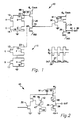
- FIG. 1 shows hot clock logic 10 for the Boolean operation of AC + BD.
- FETs 12 and 16 are connected in series, that is, the source of FET 12 is connected to the drain of FET 16.
- the logic inputs A and C are connected to the gates of FETs 12 and 16, respectively.
- inputs B and D to FETs 14 and 18, respectively result in a NAND output B .
- D ⁇ at the drain of FET 14, which goes to the gate of FET 20.
- the drains of FETs 12 and 14 are connected together thereby tying together outputs A . C ⁇ and B . D ⁇ with a NOR logic function resulting in an AND logic function result of which is equivalent to A . C + B . D, via DeMorgan's theorem, at the gate of FET 20.
- the principle of hot clock operation is based on bootstrapping of the potential at node 22 by the rising edge of a clock signal.
- the bootstrapping is caused by the parasitic capacitance between the gate and the drain of FET 20 and an optional capacitance 68.
- source follower FET 20 can turn on when the input voltage (node 22) rises (the output 38 goes to a high state -- waveform 37). If at least FETs 12 and 16 or 14 and 18 are on, the gate of FET 20 (node 22) is clamped to ground. Then the bootstrapping is overcome and FET 20 stays off.
- Circuit 11 of Figure 1 shows another configuration for input signals at E, F, G and H for the Boolean operation of (E+F) .
- (G+H) ⁇ are individual inputs to the gates of transistors 13, 15, 17 and 19, respectively.
- Node 23 can be connected to the gate of transistor 20. If circuit 11 is connected to the gate of transistor 20, then the resultant operation would be (E+F) . (G+H) ⁇ at the output on node 38 in Figure 1.
- FET 20 has its drain connected to the ⁇ 1 clock thereby pulsing its output as a source-follower comprising resistor 26 and FET 28 at node 24, the logic function output being A . C + B . D ⁇ .
- Resistive element 26 may be substituted with a FET like that of FET 48 and its connection configuration in Figure 3.
- the pulsed output of node 24 is connected to the gate of FET 30.
- the output at the drain of FET 30 is an inverted signal of that at the gate of FET 30, that is, A . C. + B . D.
- the output is connected to the gate of FET 32.
- the drain of FET 32 is connected to the ⁇ 2 clock which pulses FET 32 with a supply voltage.
- FET 32 functions as a source-follower comprising resistor 34 and FET 36 in series, having node 38 providing as an output the non-inverted signal of that at the gate of FET 32.
- Resistive element 34 may be substituted with a FET like that of FET 48 and its connection configuration in Figure 2.
- the output is pulsed with an overlap of two clocks ⁇ 1 and ⁇ 2, the output pulse being at the region of overlap of the clock pulses ⁇ 1 and ⁇ 2.
- the period of the clocks may be about 600 picoseconds.
- Signal 37 is at node 38 when the logic output is a high ("1").
- Signal 39 is at node 38 when the logic output is a low (“0").
- V ss typically is about -0.5 volt and the clock signal amplitudes range from -0.5 volt to +1.5 volts.
- Signal 37 typically varies from -0.5 volt to just a little over zero volt and signal 39 typically varies from -0.5 volt to -0.25 volt, respectively.
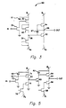
- Input buffer circuit 40 is shown in Figure 2.
- FET 30 of Figure 2 corresponds to FET 30 of Figure 1.
- FET 46 is connected in series with FET 30 and is where feedback of the ⁇ 2 clock signal is introduced.
- the drain of FET 46 that outputs an inverted signal of the input to FET 30 along with some amplitude of the feedback ⁇ 2 clock signal.
- the drain of FET 46 is connected to the gate of FET 32 which corresponds to FET 32 of Figure 1.
- the ⁇ 2 clock signal feedback to FET 46 is from node 47 and which in turn has passed through FET 42 which has the gate connected to its source. Node 47 is connected to ground through FET 44 having a gate connected to the source.
- the source of FET 42 is connected to the drain of FET 44 which has a gate and a source connected to ground or a zero reference voltage.
- the output at node 38 is that of FET 32 acting effectively as a source-follower.
- Node 38 is positioned between FET 48 which corresponds to resistor 34 of Figure 1, and FET 36 which corresponds to FET 36 of Figure 1.
- FET 48 has a gate connected to its drain and FET 36 of Figure 2 has a gate connected to its source.
- Input buffer 40 of Figure 2 has feedback to FET 46 to prevent unallowed output transitions (that is, a non-leading-edge triggered output).
- Non-inverting buffer 50 in Figure 3 together with an inverter can generate data and data signals from domino logic driven by the ⁇ 2 clock.
- FET 30 corresponds to FETs 30 in Figures 1 and 2.
- the logic output signal from node 24, which is pulsed by the ⁇ 1 clock, goes to the gate of FET 30.
- the inverted output goes on to FET 32 which corresponds to FETs 32 of Figures 1 and 2.
- the output of FET 32 is at node 38, and is like that of a source-follower.
- FETs 48 and 36 function as a voltage-divider for the output from the source of FET 32 to V ss .
- FET 48 corresponds to FET 48 of Figure 2 and to resistor 34 of Figure 1.
- At node 38 is an inversion of the input signal at the gate of transistor 30.
- Node 38 is connected to the gate of transistor 52 which inverts the signal at node 56.
- Transistor 54 having its gate connected to its source, is an active resistive element between the drain FET 52 and clock ⁇ 1. Any information transfer occurs only on the leading edge of the clock signal in circuit 50.
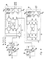
- Figure 4 is an application of the hot clock logic invention to complex circuitry.
- Adder and subtractor 58 is implemented in hot clock logic for signals M and N.
- the add and subtract carries K1′ and K2′ are generated in circuit 62 as K+′ and K-′ respectively.
- K1 and K2 have inputs which are inverted relative to K1′ and K2′ inputs, respectively.
- M′ and N′ inputs are for inverted M and N signals.
- V and V′ are the enable and disable inputs.
- Circuits 50 and 60 may be used for non-inverting and inverting inputs of M, K and V, respectively, for circuits 58 and 62.
- Circuit 50 of Figure 4 is shown in Figure 3 and described above.
- Circuit 60 is the first stage of circuit 50.
- FIG. 5 shows circuit 70 of the present invention that implements modulation doped FET (MODFET) technology.
- a logic signal may be inputted to a gate of transistor 72 which has a source connected to a zero reference voltage, and a drain connected to a gate of transistor 74.
- the principle of hot clock logic operation is effected with the bootstrapping of the potential at node 90 by the rising edge of the clock first ⁇ 1. Such bootstrapping is caused by the parasitic capacitance between the gate and drain of FET 74 and an optional capacitance 68.
- FET 72 The logic signal at the gate of FET 72 is inverted at node 90 and the signal remains inverted at node 92 as FET 74 functions as a source follower having a drain connected to the first clock ⁇ 1 and a source connected to a current control circuit incorporating FETs 76 and 78.
- FET 76 has a drain connected to node 92 and a source connected to the zero reference voltage.
- FET 78 has a drain connected to a gate of FET 76, a source connected to a second clock ⁇ 12, and an open gate.
- Node 92 is connected to a gate of FET 80.
- FET 80 has a drain connected to a gate of FET 84 and source connected to the zero reference voltage.
- Capacitor 82 is connected across the gate and drain of FET 84.
- the drain of FET 84 is connected the second clock ⁇ 2.
- the logic signal at the gate of FET 84 is an inversion of the signal at node 92.
- the signal is not inverted by FET 84 as FET 84 functions as a source follower, and the signal at output node 94 is a non-inverted, hot clock version of the input signal at the gate of FET 72.
- the source of FET 84 is connected to current control circuitry having FETs 86 and 88.
- the source of FET 84 is connected to a drain of FET 86.
- a source of FET 86 is connected to the zero reference voltage, and a drain of FET 88 is connected to a gate of FET 86.
- FET 88 has a source connected to the first clock ⁇ and has an open gate.
- circuitry of Figures 1 - 5 described above and claimed below may be implemented as optical, electrical and other types of circuitry, incorporating various media and substrates.
Landscapes
- Engineering & Computer Science (AREA)
- Power Engineering (AREA)
- Physics & Mathematics (AREA)
- Computer Hardware Design (AREA)
- Computing Systems (AREA)
- General Engineering & Computer Science (AREA)
- Mathematical Physics (AREA)
- Logic Circuits (AREA)
Applications Claiming Priority (2)
| Application Number | Priority Date | Filing Date | Title |
|---|---|---|---|
| US374196 | 1989-06-30 | ||
| US07/374,196 US4996454A (en) | 1989-06-30 | 1989-06-30 | Hot clock complex logic |
Publications (2)
| Publication Number | Publication Date |
|---|---|
| EP0405431A2 true EP0405431A2 (de) | 1991-01-02 |
| EP0405431A3 EP0405431A3 (en) | 1991-06-12 |
Family
ID=23475736
Family Applications (1)
| Application Number | Title | Priority Date | Filing Date |
|---|---|---|---|
| EP19900112097 Withdrawn EP0405431A3 (en) | 1989-06-30 | 1990-06-26 | Complex logic circuit obtaining power from clock signals |
Country Status (3)
| Country | Link |
|---|---|
| US (1) | US4996454A (de) |
| EP (1) | EP0405431A3 (de) |
| JP (1) | JPH0341822A (de) |
Families Citing this family (5)
| Publication number | Priority date | Publication date | Assignee | Title |
|---|---|---|---|---|
| WO1994002993A1 (en) * | 1992-07-17 | 1994-02-03 | Massachusetts Institute Of Technology | Recovered energy logic circuits |
| CA2151850A1 (en) * | 1994-07-18 | 1996-01-19 | Thaddeus John Gabara | Hot-clock adiabatic gate using multiple clock signals with different phases |
| CN102149537A (zh) * | 2007-07-18 | 2011-08-10 | E3生物能源有限责任公司 | 生物质和其它含碳材料超级压紧成高内能燃料 |
| US9041452B2 (en) * | 2010-01-27 | 2015-05-26 | Silicon Laboratories Inc. | Circuit and method of clocking multiple digital circuits in multiple phases |
| US9755645B1 (en) * | 2015-12-11 | 2017-09-05 | The United States Of America As Represented By The Administrator Of National Aeronautics And Space Administration | Current source logic gate |
Family Cites Families (6)
| Publication number | Priority date | Publication date | Assignee | Title |
|---|---|---|---|---|
| US3708688A (en) * | 1971-06-15 | 1973-01-02 | Ibm | Circuit for eliminating spurious outputs due to interelectrode capacitance in driver igfet circuits |
| US3866186A (en) * | 1972-05-16 | 1975-02-11 | Tokyo Shibaura Electric Co | Logic circuit arrangement employing insulated gate field effect transistors |
| DE2443490A1 (de) * | 1974-09-11 | 1976-03-25 | Siemens Ag | Schalter aus mos-transistoren |
| US4562365A (en) * | 1983-01-06 | 1985-12-31 | Commodore Business Machines Inc. | Clocked self booting logical "EXCLUSIVE OR" circuit |
| US4599528A (en) * | 1983-01-17 | 1986-07-08 | Commodore Business Machines Inc. | Self booting logical or circuit |
| US4570085A (en) * | 1983-01-17 | 1986-02-11 | Commodore Business Machines Inc. | Self booting logical AND circuit |
-
1989
- 1989-06-30 US US07/374,196 patent/US4996454A/en not_active Expired - Fee Related
-
1990
- 1990-06-21 JP JP2161490A patent/JPH0341822A/ja active Pending
- 1990-06-26 EP EP19900112097 patent/EP0405431A3/en not_active Withdrawn
Also Published As
| Publication number | Publication date |
|---|---|
| US4996454A (en) | 1991-02-26 |
| JPH0341822A (ja) | 1991-02-22 |
| EP0405431A3 (en) | 1991-06-12 |
Similar Documents
| Publication | Publication Date | Title |
|---|---|---|
| US4477737A (en) | Voltage generator circuit having compensation for process and temperature variation | |
| US5113097A (en) | CMOS level shifter circuit | |
| US5107137A (en) | Master-slave clocked cmos flip-flop with hysteresis | |
| US5880608A (en) | Pulsed domino latches | |
| US4333020A (en) | MOS Latch circuit | |
| JPS6010812A (ja) | ドライバ回路 | |
| KR960027337A (ko) | 출력신호레벨이 개선된 정논리회로 | |
| JPH035692B2 (de) | ||
| US4686396A (en) | Minimum delay high speed bus driver | |
| US4101788A (en) | Mos buffer circuit | |
| US4472645A (en) | Clock circuit for generating non-overlapping pulses | |
| EP0405431A2 (de) | Komplexe Logikschaltung mit einer von Taktsignalen bewirkten Spannungsversorgung | |
| KR960009408A (ko) | 노이즈 감소 출력 버퍼 | |
| KR940025178A (ko) | 데이터 출력회로 | |
| US4547684A (en) | Clock generator | |
| KR950010366A (ko) | 2 입력 기능들을 전부 제공하기 위한 베이스 셀 소자 | |
| US5982198A (en) | Free inverter circuit | |
| JPS598919B2 (ja) | バケツト・ブリゲ−ド・シフト・レジスタ装置 | |
| US6307416B1 (en) | Integrated circuit for producing two output clock signals at levels which do not overlap in time | |
| JP3211830B2 (ja) | Cmosレベル・シフタ回路 | |
| KR20040039581A (ko) | 출력 버퍼회로 | |
| JP2697222B2 (ja) | Cmosバッファ回路 | |
| JPS63302622A (ja) | インタフエ−ス回路 | |
| KR100280424B1 (ko) | 플립플롭 | |
| KR19990066418A (ko) | 씨모스 전압 레벨 쉬프트 회로 |
Legal Events
| Date | Code | Title | Description |
|---|---|---|---|
| PUAI | Public reference made under article 153(3) epc to a published international application that has entered the european phase |
Free format text: ORIGINAL CODE: 0009012 |
|
| AK | Designated contracting states |
Kind code of ref document: A2 Designated state(s): DE FR |
|
| PUAL | Search report despatched |
Free format text: ORIGINAL CODE: 0009013 |
|
| AK | Designated contracting states |
Kind code of ref document: A3 Designated state(s): DE FR |
|
| 17P | Request for examination filed |
Effective date: 19910826 |
|
| 17Q | First examination report despatched |
Effective date: 19940210 |
|
| STAA | Information on the status of an ep patent application or granted ep patent |
Free format text: STATUS: THE APPLICATION HAS BEEN WITHDRAWN |
|
| 18W | Application withdrawn |
Withdrawal date: 19950401 |