EP0404433A2 - Muster-Herstellungsverfahren - Google Patents
Muster-Herstellungsverfahren Download PDFInfo
- Publication number
- EP0404433A2 EP0404433A2 EP90306475A EP90306475A EP0404433A2 EP 0404433 A2 EP0404433 A2 EP 0404433A2 EP 90306475 A EP90306475 A EP 90306475A EP 90306475 A EP90306475 A EP 90306475A EP 0404433 A2 EP0404433 A2 EP 0404433A2
- Authority
- EP
- European Patent Office
- Prior art keywords
- ink
- phosphor
- pattern
- graphite
- transferring
- Prior art date
- Legal status (The legal status is an assumption and is not a legal conclusion. Google has not performed a legal analysis and makes no representation as to the accuracy of the status listed.)
- Granted
Links
Images


Classifications
-
- H—ELECTRICITY
- H01—ELECTRIC ELEMENTS
- H01J—ELECTRIC DISCHARGE TUBES OR DISCHARGE LAMPS
- H01J29/00—Details of cathode-ray tubes or of electron-beam tubes of the types covered by group H01J31/00
- H01J29/86—Vessels; Containers; Vacuum locks
- H01J29/88—Vessels; Containers; Vacuum locks provided with coatings on the walls thereof; Selection of materials for the coatings
-
- H—ELECTRICITY
- H01—ELECTRIC ELEMENTS
- H01J—ELECTRIC DISCHARGE TUBES OR DISCHARGE LAMPS
- H01J29/00—Details of cathode-ray tubes or of electron-beam tubes of the types covered by group H01J31/00
- H01J29/02—Electrodes; Screens; Mounting, supporting, spacing or insulating thereof
- H01J29/10—Screens on or from which an image or pattern is formed, picked up, converted or stored
- H01J29/18—Luminescent screens
- H01J29/30—Luminescent screens with luminescent material discontinuously arranged, e.g. in dots, in lines
- H01J29/32—Luminescent screens with luminescent material discontinuously arranged, e.g. in dots, in lines with adjacent dots or lines of different luminescent material, e.g. for colour television
- H01J29/327—Black matrix materials
-
- B—PERFORMING OPERATIONS; TRANSPORTING
- B41—PRINTING; LINING MACHINES; TYPEWRITERS; STAMPS
- B41M—PRINTING, DUPLICATING, MARKING, OR COPYING PROCESSES; COLOUR PRINTING
- B41M1/00—Inking and printing with a printer's forme
- B41M1/10—Intaglio printing ; Gravure printing
-
- G—PHYSICS
- G02—OPTICS
- G02F—OPTICAL DEVICES OR ARRANGEMENTS FOR THE CONTROL OF LIGHT BY MODIFICATION OF THE OPTICAL PROPERTIES OF THE MEDIA OF THE ELEMENTS INVOLVED THEREIN; NON-LINEAR OPTICS; FREQUENCY-CHANGING OF LIGHT; OPTICAL LOGIC ELEMENTS; OPTICAL ANALOGUE/DIGITAL CONVERTERS
- G02F1/00—Devices or arrangements for the control of the intensity, colour, phase, polarisation or direction of light arriving from an independent light source, e.g. switching, gating or modulating; Non-linear optics
- G02F1/01—Devices or arrangements for the control of the intensity, colour, phase, polarisation or direction of light arriving from an independent light source, e.g. switching, gating or modulating; Non-linear optics for the control of the intensity, phase, polarisation or colour
- G02F1/13—Devices or arrangements for the control of the intensity, colour, phase, polarisation or direction of light arriving from an independent light source, e.g. switching, gating or modulating; Non-linear optics for the control of the intensity, phase, polarisation or colour based on liquid crystals, e.g. single liquid crystal display cells
- G02F1/133—Constructional arrangements; Operation of liquid crystal cells; Circuit arrangements
- G02F1/1333—Constructional arrangements; Manufacturing methods
- G02F1/1335—Structural association of cells with optical devices, e.g. polarisers or reflectors
- G02F1/133509—Filters, e.g. light shielding masks
- G02F1/133514—Colour filters
- G02F1/133516—Methods for their manufacture, e.g. printing, electro-deposition or photolithography
-
- H—ELECTRICITY
- H01—ELECTRIC ELEMENTS
- H01J—ELECTRIC DISCHARGE TUBES OR DISCHARGE LAMPS
- H01J9/00—Apparatus or processes specially adapted for the manufacture, installation, removal, maintenance of electric discharge tubes, discharge lamps, or parts thereof; Recovery of material from discharge tubes or lamps
- H01J9/20—Manufacture of screens on or from which an image or pattern is formed, picked up, converted or stored; Applying coatings to the vessel
- H01J9/22—Applying luminescent coatings
- H01J9/227—Applying luminescent coatings with luminescent material discontinuously arranged, e.g. in dots or lines
- H01J9/2277—Applying luminescent coatings with luminescent material discontinuously arranged, e.g. in dots or lines by other processes, e.g. serigraphy, decalcomania
-
- H—ELECTRICITY
- H01—ELECTRIC ELEMENTS
- H01J—ELECTRIC DISCHARGE TUBES OR DISCHARGE LAMPS
- H01J9/00—Apparatus or processes specially adapted for the manufacture, installation, removal, maintenance of electric discharge tubes, discharge lamps, or parts thereof; Recovery of material from discharge tubes or lamps
- H01J9/20—Manufacture of screens on or from which an image or pattern is formed, picked up, converted or stored; Applying coatings to the vessel
- H01J9/22—Applying luminescent coatings
- H01J9/227—Applying luminescent coatings with luminescent material discontinuously arranged, e.g. in dots or lines
- H01J9/2278—Application of light absorbing material, e.g. between the luminescent areas
Definitions
- the present invention relates to a pattern forming method for forming fine-line patterns, and an ink composition, and more particularly to a forming method suitable forming a cathode-ray tube anode, and graphite ink and phosphor ink used in cathode-ray tube or plasma display.
- the surface of the glass substrate composing the phosphor plane was properly treated, and patterned, exposed and developed in a polyvinyl alcohol-ammonium dichromate photosensitive fluid, then a black substance such as graphite was rolled on the developed pattern, and the black matrix was formed by peeling and processing.
- the phosphor patterning was a complicated process to form each layer of R, G, B after three repeated sequences of spreading, drying, exposing, developing and drying of the slurry having the phosphor pigment dispersed in the polyvinyl alcohol-ammonium dichromate photosensitive fluid.
- an organic film layer was formed on the phosphor film as an interlayer, and the metal-backed layer was subjected to vacuum deposition. Afterwards, the glass substrate was fired at about 450°C and formed.
- the above cathode-ray tube anode forming process is very long and complicated in procedure, and requires a huge volume of water owing to wet process, and discharges much waste water containing public nuisance materials.
- edge linearity, lack of hiding, lack and other defects occurred, and it was difficult to obtain patterns of high quality. Still worse, it required an enormous plant investment because of vacuum deposition of the metal-backed layer.
- liquid crystal color panel is intensive.
- the color filter used in this liquid crystal color panel is formed mostly by the technology of photolithography, and the process was very long, including the steps of color film forming, photoresist film forming, exposing and developing, and the yield was very low and the product was hence very expensive.
- the invention is henced intended to solve the above-discussed problems, by transferring the pattern formed on a blanket of which surface is coated with an elastic material mainly composed of silicone resin, on a substrate on which a tack layer is formed, thereby forming the pattern.
- the graphite ink of the invention comprises graphite powder, vehicle containing depolymerization type organic binder, and organic acid metal salt.
- the organic binder of the graphite ink is a resin composed of at least one of poly- ⁇ -methyl styrene, poly-iso-buyl methacrylate, polymethyl methacrylate, and poly-4-fluoroethylene.
- the weight average molecular weight of the organic binder is 100,000 to 1,000 or preferably 10,000 to 1,000.
- the organic acid metal salt comprises at least one of silicon octoate, aluminum octoate, tin octoate, and zinc octoate, or at least one of silicon neodecanoate, aluminum neodecanoate, tin neodecanoate and zinc neodecanoate.
- the content of the organic acid metal salt is preferably 10 to 2 wt.%, and most preferably 6 to 2 wt.%.
- the phosphor ink of the invention comprises phosphor powder and vehicle containing depolymerization type organic binder.
- the organic binder of the phosphor ink is a resin composed of at least one of poly- ⁇ -methyl styrene, poly-isobutyl methacrylate, polymethyl methacrylate and poly-4-fluoroethylene.
- the weight average molecular weight of the organic binder is 100,000 to 1,000, or preferably 40,000 to 1,000.
- the organic solvent in the ink comprises at least one of ⁇ -terpineol, n-butylcarbitol, n-butylcarbitol acetate, 2,2,4-trimethyl-1,3-hydroxypentyl-iso-butylate, linseed oil, and ethylene glycol monophenyl ether.
- the content of this organic solvent is preferably 12:10 to 16:10 by weight to the graphite powder content in the graphite ink, and 1.5:10 to 3.0:10 by weight to the phosphor powder content in the phosphor ink.
- the forming method of cathode-ray tube anode of the invention comprises a step of filling the groove of the intaglio with graphite ink, a step of transferring the graphite ink in the groove of the intaglio onto the blanket of which surface is coated with an elastic material mainly composed of silicone resin, a step of forming a tack layer on the substrate, a step of transferring and printing the pattern transferred on the blanket onto the substrate, a step of filling the groove of the intaglio with phosphor ink, a step of transferring the ink in the groove of the intaglio onto the blanket of which surface is coated with an elastic material mainly composed of silicone resin, a step of forming a tack layer on the substrate, a step of transferring the pattern transferred on the blanket onto a substrate on which graphite pattern has been formed, a step of transferring an aluminum thin film possessing multiple holes so as to cover the black matrix and phosphor layer as metal-backed layer, and a step
- the ink characteristics such as fluidity and tackiness necessary for transfer from blanket to substrate are not limited, and a wide range of materials may be used as the pattern forming material. That is, very fine-line thick film patterns may be formed easily on the substrate, and when this method is employed in formation of phosphor plane for CRT or plasma display, very fine-line graphite pattern and phosphor pattern may be easily formed on the substrate. This method is also free from problems experienced in the conventional wet process, that is, use of large volume of water and discharge of waste water containing public nuisance materials. Still more, vacuum deposition is not needed. Therefore, the manufacturing cost may be reduced greatly. From the viewpoint of precision, patterns of high quality are obtained. Furthermore, the black matrix and phosphor layer strong in the adhesive strength with the glass surface are formed, and a cathode-ray tube of high reliability may be presented.
- the invention is characterized by formation of fine-line thick film patterns by transferring the patterns formed on the blanket of which surface is coated with an elastic material mainly composed of silicone resin onto a substrate on which a tack layer is formed.
- an elastic material mainly composed of silicone resin By simplifying the process, the cost may be notably reduced.
- this technique is applied in cathode-ray tube, plasma display or other phosphor products, or liquid crystal color filter and other pattern products, inexpensive products of high quality may be obtained without requiring any large manufacturing equipment.
- the invention also features a graphite ink comprising graphite powder, vehicle containing depolymerization type organic binder and organic acid metal salt, a phosphor ink composed of phosphor powder and vehicle containing depolymerization type organic binder, and formation of print pattern by offset printing by using said graphite ink and phosphor ink.
- a graphite ink comprising graphite powder, vehicle containing depolymerization type organic binder and organic acid metal salt, a phosphor ink composed of phosphor powder and vehicle containing depolymerization type organic binder, and formation of print pattern by offset printing by using said graphite ink and phosphor ink.
- the graphite ink and phosphor ink instead of the vacuum deposition process of the metal- backed layer, it is possible to fire after transferring and forming before firing the aluminum thin film possessing multiple pores, so that the process may be further simplified.
- the cost reduction rate may reach up to 1/10, and when this method is applied in pattern products such as cathode-ray tubes, plasma displays and phosphor products, products of high quality may be obtained at low cost without requiring large manufacturing facilities.
- the black matrix and phosphor layer strong in adhesive strength to the glass surface are formed, and cathode-ray tubes of high reliability may be presented.
- Fig. 1 is an explanatory drawing of the pattern forming method of the invention.
- numeral 101 is a substrate.
- Numeral 102 is a tack layer formed in order to enhance the printability when forming patterns, which may be either a tacky adhesive material at ordinary temperature or a thermoplastic resin to be used in tacky adhesive state by heating and melting. Or by using a tacky adhesive material which is cured by ultraviolet rays, the pattern of a specific part may be solidified.
- Numeral 103 is a blanket of which surface is coated with a rubber-like elastic body with a favorable parting property, and among silicone resins, fluoroplastics and polyethylene resins, what is preferably used in an elastic material with JIS rubber hardness of 30 to 60 degrees, mainly composed of silicone resin, having the surface covered in a thickness of about 5 mm.
- Numeral 104 is a pattern formed on the blanket, in which ink is dropped into the gravure intaglio, the entire surface of the gravure intaglio is scraped by a scraper to leave the ink only in the groove, and the blanket is pressed against the surface to transfer the pattern.
- Numeral 105 is a desired pattern obtained by pressing and transferring the pattern on the blanket onto the substrate on which the tack layer has been formed.
- the pattern 104 on the blanket may be formed by using a letterpress or by screen printing, as well as by transfer from the intaglio.
- a pattern product As a product requiring pattern (hereinafter called a pattern product), an example of anode formation of color cathode-ray tube is presented and embodiments of graphite ink, phosphor ink and forming method of cathode-ray tube anode of the invention are described below while referring to the accompanying drawings.
- Fig. 2 is a sectional view of a color cathode-ray tube anode, in which a black matrix 202 made of a black substance and a phosphor layer 203 are formed inside a glass-made face plate 201, and a metal-backed layer 204 is disposed.
- the metal-backed layer 204 is intended to enhance the luminance by reflecting the light emitted from the phosphor plane by the mirror action of the metal film.
- the aluminum thin film having multiple pores is transferred and formed before firing.
- the one-minute flow value of the prepared ink on a spread meter was 13 mm, and by using this graphite ink, a stripe of 65 ⁇ m in width and 4 ⁇ m in height was printed on a glass plate.
- the printing method is shown below.
- the tacky adhesive material (isodecylmethacrylate, glass transition point -60°C, 30% toluene solution) was applied on the glass plate by spin coating in a thickness of 2 ⁇ m, and dried to obtain the transfer object.
- the tacky adhesive material should be preferably a material that is adhesive at ordinary temperature and is completely pyrolyzed in the binder removal process at the final step, and an acrylic resin with the glass transition point of 40°C or less was favorable.
- the intaglio was a stainless steel plate having stripe etching of 70 ⁇ m in width and 15 ⁇ m in depth, and the graphite ink was dropped on the intaglio, and the whole surface of the intaglio was scraped off by a ceramic scraper to leave the graphite ink only in a groove of the intaglio, and the blanket having the surface coated with silicone rubber (JIS rubber hardness 35 degrees) in a thickness of 5 mm was pressed and rotated to transfer the pattern on the transfer object.
- the obtained pattern was excellent in linearity, and had a high quality, being free from lack of hiding, lack or other defects.
- the hardness of the silicone rubber covering the surface of the blanket is very low (less than 10 degrees) such as in the case of Pad printing, the deformation of the rubber-like elastic material becomes very large, and the intaglio pattern cannot be reproduced reliably, or if the hardness is too high, the contact between the blanket and ink is poor, and the pattern cannot be reproduced reliably, too.
- the proper hardness of the elastic material for covering the surface was 30 degrees or more as the JIS rubber hardness, and preferably in a range of 35 to 60 degrees.
- red phosphor ink and blue phosphor ink were prepared.
- a stainless steel etching plate of 145 ⁇ m in width and 40 ⁇ m in depth was used, and a green phosphor pattern was printed on a glass plate in a same gravure offset method as in the preceding example.
- the red phosphor ink and blue phosphor ink were printed in specified positions, and a three-color phosphor pattern of red, green and blue was obtained.
- the printed pattern satisfied all of stripe uniformity, linearity and film thickness precision.
- Graphite (Hitachi Powder Metal Co., GP-60S) 24 (parts by weight) Mean particle size 0.4 ⁇ m - i-BMA, ⁇ -MeSt resin (Sekisui Chemical Co., IBS-6) 32 Weight average molecular weight 4750 - Solvent (Kanto Chemical Co., n-butylcarbitol acetate) 32 - Adhesive agent (silicon octoate) 5 - Dispersing agent (Toho Chemical Co., Dispant EN-120A) 3 - Linseed oil 4
- An acrylic tacky adhesive material with the glass transition point of -2°C (a copolymer of isobutylmethacrylate and glycidyl methacrylate) was applied on a glass substrate and dried, and a tack layer of 3 ⁇ m was formed.
- a black stripe pattern was printed on the glass substrate on which the tack layer is formed, in the printing conditions of intaglio (60 ⁇ m in width, 20 ⁇ m in depth) and blanket (rubber hardness 45 degrees, silicone rubber, rubber thickness 6 mm).
- the printed black stripe pattern was 55 ⁇ m in width and 5 ⁇ m in thickness, and a favorable linearity was confirmed.
- Example 2 using a ceramic three roll mill, the mill base of the following composition was passed six times to mix, and a phosphor ink was prepared.
- red luminescent phosphor and ZnS:Ag as red luminescent phosphor
- a red phosphor ink and a blue phosphor ink were prepared.
- the intaglio a stainless steel etching plate of 145 in width and 40 ⁇ m in depth was used, and the green phosphor pattern was printed on the glass plate by the same offset gravure method as in Example 1.
- the red phosphor ink and blue phosphor ink were printed at specified positions, and a three-color phosphor pattern of red, green and blue was obtained.
- the printed pattern satisfied all of the stripe uniformity, linearity and film thickness precision.
- the metal-backed layer multiple fine pores were opened in an aluminum thin film of 1500 angstroms in thickness evaporated on a PET film, and it was pressed with a pressure of 3 kg/mm2 to transfer on the black matrix and phosphor pattern.
- This substrate was fired at 450°C, and the organic matter was burnt out, and a sufficient optical characterization was obtained as a color cathode-ray tube anode.
- phosphor plane was free from dropout of phosphor, lack of hiding, lack and other defects because exposure and development were not repeated as in the conventional wet process, and the phosphor plane of high quality was obtained.
- the procedure is simplified, and the number of steps is decreased.
- the phosphor is free from deterioration due to chrome ions such as ammonium dichromate, and a pattern of uniform thickness of 10 to 12 ⁇ m which is said to be an ideal film thickness for the phosphor is obtained, so that a cathode-ray tube of about 10% brighter as compared with the prior art is realized.
- the phosphor plane obtained in this manner was satisfactory as the anode for cathode-ray tube or plasma display.
- Fig. 2 shows a curve 201 of the amount of exhaust gas (40°C, 1 hour) from the formed cathode-ray tube anode, in terms of the ratio of polymerization of iso-butyl methacrylate and ⁇ -methyl styrene.
- the degree of vacuum applicable as the cathode-ray tube anode is in the order to 10 ⁇ 7 to 10 ⁇ 6, and as known from the diagram, ⁇ -methyl styrene was 5 to 20 wt.% in the region where the amount of the exhaust gas was in the order of 10 ⁇ 6.
- Fig. 3 is a transfer amount diagram showing the transfer amount curve 301 of the phosphor ink to the transfer object, together with the organic solvent/phosphor powder amount ratio (by weight) when the phosphor powder and organic solvent in Example 2 are used.
- the region of the largest transfer amount was the region of the organic solvent/phosphor powder ratio (by weight) of 0.15 to 0.30.
- the organic solvent/graphite powder amount ratio (by weight) of the graphite ink was 1.2 to 1.6.
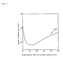
- Fig. 4 shows the weight loss curve 401 showing the relation between the weight loss immediately after firing and the content of silicone octoate in the graphite ink in the case of washing and drying of cathode-ray tube anode (25 cm2) in running water with water pressure of 0.1 kg/cm2 and water flow of 1200 ml/min.
- the weight loss was less at the silicon octoate of 10 to 2 wt.%, and it is known that the adhesive strength is markedly increased.
- the most preferable content of silicon octoate was 6 to 2 wt.%.
- Example 1 and Example 2 As the resin, meanwhile, in Example 1 and Example 2, a copolymer of iso-butyl methacrylate (iBA) and poly- ⁇ -methyl styrene ( ⁇ -MeSt), and a copolymer of poly-iso-butyl methacrylate (iBMA), polymethyl methacrylate and poly- ⁇ -methyl styrene ( ⁇ -MeSt) were used, but individual monomers may be also used.
- iBA iso-butyl methacrylate
- ⁇ -MeSt poly- ⁇ -methyl styrene
- iBMA poly-iso-butyl methacrylate
- ⁇ -MeSt polymethyl methacrylate
- ⁇ -MeSt poly- ⁇ -methyl styrene
- acrylic resin for example, n-butyl methacrylate
- the scattering performance was poor, and it was not practicable.
- polytetrafluoroethylene or polybutene it is also possible to use polytetrafluoroethylene or polybutene. This is possible, of course, in consideration of the miscibility of resins and dissolution amount into the solvent.
- glycidyl methacrylate or the like may be copolymerized within 5%.
- the resin In the resin, however, it is required to contain ⁇ -methyl styrene by at least 5 to 20 wt.%, and out of this range or with the acrylic resin alone, the scattering performance of the resin is poor, and the degree of vacuum of the formed cathode-ray tube deteriorates.
- the average molecular weight of the resin if the average molecular weight of the resin is more than 100,000, the ink viscosity becomes high, which is not suited to printing, or if less than 1000, the scattering performance in firing is worse. That is, the average molecular weight of the resin should be preferably at 100,000 to 1,000 or more preferably 10,000 to 1,000.
- Example 1 and Example 3 As the organic solvent, in Example 1 and Example 3, butylcarbitol acetate was used, and ⁇ -terpineol in Example 2, but these are not limitative, and butylcarbitol, 2,2,4-trimethyl-1-3-hydroxybentyl isobutylate, and ethyleneglycol monophenyl ether may be used either alone or in combination, which may be selected depending on the printing condition and drying condition.
- silicon octoate was used in Example 1 and Example 2, but it is not limitative, and as the organic acid metal salt, at least one of silicon octoate, aluminum octoate, tin octoate and zinc octoate, or at least one of silicon neodecanoate, aluminum neodecanoate, tin neodecanoate and zinc neodecanoate may be used, and the contents of these organic acid metal salts may be preferably 10 to 2 wt.% in consideration of the scattering performance of the resin, and the most preferable content is 6 to 2 wt.%.
- Example 1 and Example 2 powder with average particle size of 0.4 ⁇ m was used, but the average particle size may be sufficient in a range of 0.2 to 1.0 ⁇ m.
- the average particle size of 5.2 ⁇ m is used, but this value is not limitative, and the average particle size of 2.0 to 15.0 ⁇ m is applicable.
- red, green and blue phosphor powders were used, but as the blue luminescent phosphor, either the pigmented phosphor combined with blue pigment, such as cobalt blue pigment, or the phosphor alone may be used.
- the green luminescent phosphor either the pigmented phosphor combined with green pigment, such as chromium oxide pigment, or the phosphor alone may be used.
- the phosphor powder as far as it is applicable to phosphor for television, display, projection tube and special tube or the like, for example, not only Y2O2S:Eu phosphor stated above, but also Y2O3:Eu, YVO4:Eu, CaS:Eu or the like may be used as the red luminescent phosphor, Zn2SiO4:Mn, As, (Y, Gd)2O2S:Tb, InBO3:Tb, Y2SiO5:Tb, LaOCl:Tb or the like as the green luminescent phosphor, Y2SiO5:Ce, (SrCaBa)5 (PO4)3Cl:Eu or the like as the blue luminescent phosphor, and InBO3:Eu or the like as the orange luminescent
- blue ink and green ink were also prepared by using different pigments.
- an ultraviolet setting resin (Goselac, Nippon Gosei Kagaku Co.) was formed on a glass substrate.
- an ultraviolet setting resin Goselac, Nippon Gosei Kagaku Co.
- inks for color filter in the composition above After printing in the conditions of gravure intaglio (width 120 ⁇ m, depth 15 ⁇ m) and blanket (silicone rubber hardness 45 degrees, rubber thickness 8 mm), ultraviolet emitted to cure, and a pattern with excellent lincarity of 100 ⁇ m was obtained. These patterns of three colors were excellent as the color filter for liquid crystal.
Landscapes
- Physics & Mathematics (AREA)
- Engineering & Computer Science (AREA)
- Manufacturing & Machinery (AREA)
- Nonlinear Science (AREA)
- Mathematical Physics (AREA)
- Chemical & Material Sciences (AREA)
- Crystallography & Structural Chemistry (AREA)
- General Physics & Mathematics (AREA)
- Optics & Photonics (AREA)
- Formation Of Various Coating Films On Cathode Ray Tubes And Lamps (AREA)
- Inks, Pencil-Leads, Or Crayons (AREA)
- Printing Methods (AREA)
Applications Claiming Priority (4)
| Application Number | Priority Date | Filing Date | Title |
|---|---|---|---|
| JP156513/89 | 1989-06-19 | ||
| JP1156513A JPH0322324A (ja) | 1989-06-19 | 1989-06-19 | パターン形成方法およびパターン製品 |
| JP49743/90 | 1990-03-01 | ||
| JP2049743A JPH03252466A (ja) | 1990-03-01 | 1990-03-01 | グラファイトインキ、蛍光体インキならびに陰極線管アノードの形成方法 |
Publications (3)
| Publication Number | Publication Date |
|---|---|
| EP0404433A2 true EP0404433A2 (de) | 1990-12-27 |
| EP0404433A3 EP0404433A3 (de) | 1991-11-27 |
| EP0404433B1 EP0404433B1 (de) | 1996-10-23 |
Family
ID=26390194
Family Applications (1)
| Application Number | Title | Priority Date | Filing Date |
|---|---|---|---|
| EP90306475A Expired - Lifetime EP0404433B1 (de) | 1989-06-19 | 1990-06-14 | Muster-Herstellungsverfahren |
Country Status (4)
| Country | Link |
|---|---|
| US (1) | US5635006A (de) |
| EP (1) | EP0404433B1 (de) |
| KR (1) | KR930002651B1 (de) |
| DE (1) | DE69028950T2 (de) |
Cited By (3)
| Publication number | Priority date | Publication date | Assignee | Title |
|---|---|---|---|---|
| EP0778153A1 (de) * | 1995-12-05 | 1997-06-11 | Sumitomo Chemical Company, Limited | Verbundfolie, die durch Tiefdruck hergestellt wird |
| KR19980020318A (ko) * | 1996-09-06 | 1998-06-25 | 손욱 | 음극선관 블랙 매트릭스 패턴 형성용 토너 조성물 및 이를 이용한 블랙 매트릭스 패턴의 형성방법 |
| EP0836892A3 (de) * | 1996-10-21 | 1999-09-08 | Dai Nippon Printing Co., Ltd. | Übertragungsschicht und Verfahren zur Herstellung eines Musters |
Families Citing this family (8)
| Publication number | Priority date | Publication date | Assignee | Title |
|---|---|---|---|---|
| AU4767096A (en) * | 1995-01-25 | 1996-08-14 | Northern Engraving Corporation | Improved fluorescent inks |
| JPH1027550A (ja) * | 1996-05-09 | 1998-01-27 | Pioneer Electron Corp | プラズマディスプレイパネル |
| US6251208B1 (en) * | 1996-10-29 | 2001-06-26 | Toshiba Machine Co., Ltd. | Method for manufacturing a structure with fine ribs |
| GB0110977D0 (en) * | 2001-05-04 | 2001-06-27 | Vecht Aron | Phosphor layers for electroluminescent panels and methods of their manufacture |
| KR100860521B1 (ko) * | 2001-12-28 | 2008-09-26 | 엘지디스플레이 주식회사 | 컬러필터 형성용 인쇄장치 및 컬러필터 형성방법 |
| KR100870611B1 (ko) * | 2004-09-10 | 2008-11-25 | 가부시키가이샤 슈호 | 곡면에의 인쇄 방법 및 그에 의한 인쇄 곡면체 |
| KR101212151B1 (ko) * | 2005-12-29 | 2012-12-13 | 엘지디스플레이 주식회사 | 패턴 형성 방법을 이용한 액정표시소자 제조방법 |
| KR20080095385A (ko) * | 2007-04-24 | 2008-10-29 | 엘지전자 주식회사 | 플라즈마 디스플레이 패널 및 그 제조방법 |
Family Cites Families (9)
| Publication number | Priority date | Publication date | Assignee | Title |
|---|---|---|---|---|
| US3821009A (en) * | 1972-04-28 | 1974-06-28 | Zenith Radio Corp | Method of aluminizing a cathode-ray tube screen |
| US3993842A (en) * | 1973-04-24 | 1976-11-23 | E. I. Du Pont De Nemours And Company | Electrically conductive elastomeric ink |
| US4209551A (en) * | 1977-12-28 | 1980-06-24 | Toppan Printing Co., Ltd. | Method of fabricating a phosphor screen of a color television picture tube |
| JPS5541671A (en) * | 1978-09-19 | 1980-03-24 | Sumitomo Electric Industries | Method of forming terminal at bus bar used for switch box |
| JPS5546674A (en) * | 1978-09-30 | 1980-04-01 | Pioneer Electronic Corp | Speaker specification unit for coaxial speaker |
| DE2921238C3 (de) * | 1979-05-25 | 1982-02-04 | Degussa Ag, 6000 Frankfurt | Verfahren zur Herstellung von leichtdispergierbaren Pigmentpräparationen |
| JPS5633820A (en) * | 1979-08-29 | 1981-04-04 | Toshiba Corp | Device for ion implantation |
| US4608301A (en) * | 1983-08-02 | 1986-08-26 | Fuji Photo Film Co., Ltd. | Radiographic intensifying screen |
| JPH0680577B2 (ja) * | 1985-11-08 | 1994-10-12 | 株式会社東芝 | カラ−受像管の蛍光面形成方法 |
-
1990
- 1990-06-14 DE DE69028950T patent/DE69028950T2/de not_active Expired - Fee Related
- 1990-06-14 EP EP90306475A patent/EP0404433B1/de not_active Expired - Lifetime
- 1990-06-19 KR KR1019900009008A patent/KR930002651B1/ko not_active Expired - Fee Related
- 1990-06-19 US US07/540,622 patent/US5635006A/en not_active Expired - Fee Related
Cited By (4)
| Publication number | Priority date | Publication date | Assignee | Title |
|---|---|---|---|---|
| EP0778153A1 (de) * | 1995-12-05 | 1997-06-11 | Sumitomo Chemical Company, Limited | Verbundfolie, die durch Tiefdruck hergestellt wird |
| US5942298A (en) * | 1995-12-05 | 1999-08-24 | Sumitomo Chemical Company, Limited | Laminated film |
| KR19980020318A (ko) * | 1996-09-06 | 1998-06-25 | 손욱 | 음극선관 블랙 매트릭스 패턴 형성용 토너 조성물 및 이를 이용한 블랙 매트릭스 패턴의 형성방법 |
| EP0836892A3 (de) * | 1996-10-21 | 1999-09-08 | Dai Nippon Printing Co., Ltd. | Übertragungsschicht und Verfahren zur Herstellung eines Musters |
Also Published As
| Publication number | Publication date |
|---|---|
| EP0404433A3 (de) | 1991-11-27 |
| KR930002651B1 (ko) | 1993-04-07 |
| KR910001860A (ko) | 1991-01-31 |
| US5635006A (en) | 1997-06-03 |
| DE69028950T2 (de) | 1997-04-30 |
| EP0404433B1 (de) | 1996-10-23 |
| DE69028950D1 (de) | 1996-11-28 |
Similar Documents
| Publication | Publication Date | Title |
|---|---|---|
| US4209551A (en) | Method of fabricating a phosphor screen of a color television picture tube | |
| DE3625014C1 (de) | Verfahren zur Herstellung von Bildern auf tonbaren lichtempfindlichen Schichten | |
| US5635006A (en) | Pattern forming method and ink compostion | |
| EP0027612B1 (de) | Fotopolymerisierbare Gemische und daraus hergestellte lichthärtbare Elemente | |
| EP0481548A1 (de) | Gemusterter Empfänger für Farbfilteranordnung | |
| DE69819445T2 (de) | Verfahren zur Herstellung eines Musters auf einem Substrat | |
| EP0523245A1 (de) | Herstellungsverfahren für vielfarbenanzeigegerät | |
| KR100655945B1 (ko) | 전계방출디스플레이패널용형광체패턴의제조방법,전계방출디스플레이패널용감광성소자,전계방출디스플레이패널용형광체패턴및전계방출디스플레이패널 | |
| EP0432713B1 (de) | Verfahren zur Herstellung von Bildern auf tonbaren lichtempfindlichen Schichten | |
| US5658697A (en) | Method for producing color filters by the use of anionic electrocoats | |
| EP0785565A1 (de) | Phosphormuster, Verfahren zur Herstellung desselben und lichtempfindliches verwendetes Element dafür | |
| US4651053A (en) | Display tube having printed copolymer film layer | |
| KR20040030236A (ko) | 도전성 페이스트 조성물, 전극 형성용 전사 필름 및플라즈마 디스플레이 패널용 전극 | |
| GB2034910A (en) | Process for forming phosphor screens | |
| KR940007138B1 (ko) | 형광체 잉크 | |
| US5756241A (en) | Self-aligned method for forming a color display screen | |
| JPH04357026A (ja) | 粘着層転写シート及びパターン形成方法 | |
| KR20000038860A (ko) | 칼라 음극선관의 형광면 형성방법 | |
| JPH0834947A (ja) | 蛍光体インキ組成物 | |
| JPH0322324A (ja) | パターン形成方法およびパターン製品 | |
| JPH03252466A (ja) | グラファイトインキ、蛍光体インキならびに陰極線管アノードの形成方法 | |
| JP3900597B2 (ja) | 感光性ペースト | |
| Kim et al. | New Barrier Rib Forming Method for PDP Fabrication | |
| KR19990012416A (ko) | 접착력 보강 형광막용 슬러리 및 형광막 패턴 형성 방법 | |
| JPS624811B2 (de) |
Legal Events
| Date | Code | Title | Description |
|---|---|---|---|
| PUAI | Public reference made under article 153(3) epc to a published international application that has entered the european phase |
Free format text: ORIGINAL CODE: 0009012 |
|
| AK | Designated contracting states |
Kind code of ref document: A2 Designated state(s): DE FR GB NL |
|
| PUAL | Search report despatched |
Free format text: ORIGINAL CODE: 0009013 |
|
| AK | Designated contracting states |
Kind code of ref document: A3 Designated state(s): DE FR GB NL |
|
| 17P | Request for examination filed |
Effective date: 19920518 |
|
| 17Q | First examination report despatched |
Effective date: 19940223 |
|
| GRAH | Despatch of communication of intention to grant a patent |
Free format text: ORIGINAL CODE: EPIDOS IGRA |
|
| GRAH | Despatch of communication of intention to grant a patent |
Free format text: ORIGINAL CODE: EPIDOS IGRA |
|
| GRAA | (expected) grant |
Free format text: ORIGINAL CODE: 0009210 |
|
| AK | Designated contracting states |
Kind code of ref document: B1 Designated state(s): DE FR GB NL |
|
| REF | Corresponds to: |
Ref document number: 69028950 Country of ref document: DE Date of ref document: 19961128 |
|
| ET | Fr: translation filed | ||
| PLBE | No opposition filed within time limit |
Free format text: ORIGINAL CODE: 0009261 |
|
| STAA | Information on the status of an ep patent application or granted ep patent |
Free format text: STATUS: NO OPPOSITION FILED WITHIN TIME LIMIT |
|
| 26N | No opposition filed | ||
| REG | Reference to a national code |
Ref country code: GB Ref legal event code: IF02 |
|
| PGFP | Annual fee paid to national office [announced via postgrant information from national office to epo] |
Ref country code: FR Payment date: 20040608 Year of fee payment: 15 |
|
| PGFP | Annual fee paid to national office [announced via postgrant information from national office to epo] |
Ref country code: GB Payment date: 20040609 Year of fee payment: 15 |
|
| PGFP | Annual fee paid to national office [announced via postgrant information from national office to epo] |
Ref country code: DE Payment date: 20040624 Year of fee payment: 15 |
|
| PGFP | Annual fee paid to national office [announced via postgrant information from national office to epo] |
Ref country code: NL Payment date: 20050605 Year of fee payment: 16 |
|
| PG25 | Lapsed in a contracting state [announced via postgrant information from national office to epo] |
Ref country code: GB Free format text: LAPSE BECAUSE OF NON-PAYMENT OF DUE FEES Effective date: 20050614 |
|
| PG25 | Lapsed in a contracting state [announced via postgrant information from national office to epo] |
Ref country code: DE Free format text: LAPSE BECAUSE OF NON-PAYMENT OF DUE FEES Effective date: 20060103 |
|
| PG25 | Lapsed in a contracting state [announced via postgrant information from national office to epo] |
Ref country code: FR Free format text: LAPSE BECAUSE OF NON-PAYMENT OF DUE FEES Effective date: 20060228 |
|
| GBPC | Gb: european patent ceased through non-payment of renewal fee |
Effective date: 20050614 |
|
| REG | Reference to a national code |
Ref country code: FR Ref legal event code: ST Effective date: 20060228 |
|
| PG25 | Lapsed in a contracting state [announced via postgrant information from national office to epo] |
Ref country code: NL Free format text: LAPSE BECAUSE OF NON-PAYMENT OF DUE FEES Effective date: 20070101 |
|
| NLV4 | Nl: lapsed or anulled due to non-payment of the annual fee |
Effective date: 20070101 |