EP0398552B1 - Architecture d'intégration à l'échelle de la plaquette pour un réseau à interconnexion linéaire - Google Patents
Architecture d'intégration à l'échelle de la plaquette pour un réseau à interconnexion linéaire Download PDFInfo
- Publication number
- EP0398552B1 EP0398552B1 EP90304801A EP90304801A EP0398552B1 EP 0398552 B1 EP0398552 B1 EP 0398552B1 EP 90304801 A EP90304801 A EP 90304801A EP 90304801 A EP90304801 A EP 90304801A EP 0398552 B1 EP0398552 B1 EP 0398552B1
- Authority
- EP
- European Patent Office
- Prior art keywords
- cell
- logic
- selection
- boundary
- cells
- Prior art date
- Legal status (The legal status is an assumption and is not a legal conclusion. Google has not performed a legal analysis and makes no representation as to the accuracy of the status listed.)
- Expired - Lifetime
Links
- 230000010354 integration Effects 0.000 title description 15
- 230000006870 function Effects 0.000 claims description 44
- 238000004891 communication Methods 0.000 claims description 7
- 230000001413 cellular effect Effects 0.000 claims description 3
- 239000004065 semiconductor Substances 0.000 claims description 2
- 238000010276 construction Methods 0.000 claims 1
- 210000004027 cell Anatomy 0.000 description 315
- CIWBSHSKHKDKBQ-JLAZNSOCSA-N Ascorbic acid Chemical compound OC[C@H](O)[C@H]1OC(=O)C(O)=C1O CIWBSHSKHKDKBQ-JLAZNSOCSA-N 0.000 description 14
- 238000013459 approach Methods 0.000 description 14
- 238000000034 method Methods 0.000 description 11
- 238000012360 testing method Methods 0.000 description 7
- 238000013461 design Methods 0.000 description 6
- 238000003491 array Methods 0.000 description 5
- 238000004519 manufacturing process Methods 0.000 description 5
- 230000008901 benefit Effects 0.000 description 4
- 238000010586 diagram Methods 0.000 description 4
- 230000001360 synchronised effect Effects 0.000 description 4
- 230000002950 deficient Effects 0.000 description 3
- 230000001934 delay Effects 0.000 description 3
- 230000000694 effects Effects 0.000 description 3
- 238000003306 harvesting Methods 0.000 description 3
- 238000012986 modification Methods 0.000 description 3
- 230000004048 modification Effects 0.000 description 3
- 230000002093 peripheral effect Effects 0.000 description 3
- 230000011664 signaling Effects 0.000 description 3
- 210000004460 N cell Anatomy 0.000 description 2
- 230000015572 biosynthetic process Effects 0.000 description 2
- 239000000872 buffer Substances 0.000 description 2
- 230000007547 defect Effects 0.000 description 2
- 238000005755 formation reaction Methods 0.000 description 2
- 230000006386 memory function Effects 0.000 description 2
- 238000004806 packaging method and process Methods 0.000 description 2
- 230000000737 periodic effect Effects 0.000 description 2
- 230000004044 response Effects 0.000 description 2
- 239000007787 solid Substances 0.000 description 2
- 238000003860 storage Methods 0.000 description 2
- 238000012546 transfer Methods 0.000 description 2
- 241000221931 Hypomyces rosellus Species 0.000 description 1
- 238000010420 art technique Methods 0.000 description 1
- 230000002457 bidirectional effect Effects 0.000 description 1
- 210000003888 boundary cell Anatomy 0.000 description 1
- 230000003111 delayed effect Effects 0.000 description 1
- 230000006872 improvement Effects 0.000 description 1
- 230000001788 irregular Effects 0.000 description 1
- 238000005192 partition Methods 0.000 description 1
- 230000010363 phase shift Effects 0.000 description 1
- 238000012545 processing Methods 0.000 description 1
- 230000009467 reduction Effects 0.000 description 1
- 230000002441 reversible effect Effects 0.000 description 1
- 238000012552 review Methods 0.000 description 1
- 238000012956 testing procedure Methods 0.000 description 1
Images


Classifications
-
- H—ELECTRICITY
- H03—ELECTRONIC CIRCUITRY
- H03K—PULSE TECHNIQUE
- H03K19/00—Logic circuits, i.e. having at least two inputs acting on one output; Inverting circuits
- H03K19/02—Logic circuits, i.e. having at least two inputs acting on one output; Inverting circuits using specified components
- H03K19/173—Logic circuits, i.e. having at least two inputs acting on one output; Inverting circuits using specified components using elementary logic circuits as components
- H03K19/1733—Controllable logic circuits
- H03K19/1737—Controllable logic circuits using multiplexers
-
- G—PHYSICS
- G11—INFORMATION STORAGE
- G11C—STATIC STORES
- G11C29/00—Checking stores for correct operation ; Subsequent repair; Testing stores during standby or offline operation
- G11C29/006—Checking stores for correct operation ; Subsequent repair; Testing stores during standby or offline operation at wafer scale level, i.e. wafer scale integration [WSI]
-
- H—ELECTRICITY
- H03—ELECTRONIC CIRCUITRY
- H03K—PULSE TECHNIQUE
- H03K19/00—Logic circuits, i.e. having at least two inputs acting on one output; Inverting circuits
- H03K19/02—Logic circuits, i.e. having at least two inputs acting on one output; Inverting circuits using specified components
- H03K19/173—Logic circuits, i.e. having at least two inputs acting on one output; Inverting circuits using specified components using elementary logic circuits as components
- H03K19/1733—Controllable logic circuits
- H03K19/1735—Controllable logic circuits by wiring, e.g. uncommitted logic arrays
- H03K19/1736—Controllable logic circuits by wiring, e.g. uncommitted logic arrays in which the wiring can be modified
Definitions
- This invention is directed to an architecture for interconnecting an array, and in particular to use of that architecture to construct a linear array from a wafer scale integrated array of substantially identically formed cells.
- VLSI very large scale integration
- Wafer scale integration seeks to assemble an entire system on a single wafer, rather than partition the wafer into chips that each carry smaller portions of a system, and thereby requires the expense of individual packaging.
- yield has been one problem that works against successful wafer scale integration. Fabrication flaws must be overcome in order to effectively and economically use wafer scale integration techniques.
- Another approach and one to which the present invention is directed, involves forming a multiplicity of substantially identical circuits or cells on a wafer.
- Each cell contains logic for performing one or more functions (e.g., arithmetic and/or logic functions, memory functions, or any combination of these and other functions).
- Various techniques are then used for interconnecting these cells.
- connection techniques known today are (1) imbedding the cells in a sea of switches to interconnect them in various fashions (i.e., to form 2-D meshes, linear arrays, tree configuration, and the like) using fuses or switches that are set during manufacture; or (2) interconnecting the cells with cross-bar switches, connecting every pair of cells. Examples of these kinds of wafer scale integration formations can be seen in W.R. Moore, “A Review of Fault Tolerant Techniques for the Enhancement of Integrated Circuit Yield," Proc. of the IEEE , Vol. 74, May, 1986, pp. 684-698; W.
- a more practical cell interconnection approach has been to provide separate inputs and outputs between a cell and each of its neighbors to increase interconnection flexibility.
- the cell carries a logic function whose input may be selected from any one of the four neighbors, and whose output is, in turn, communicated to the selection logic associated with each boundary (which also receives inputs from each of the other boundaries).
- the amount of logic to implement the selection logic may take up a significant area of the cell, and particularly so when the information is communicated in parallel instead of bit serial form.
- the routing of the necessary signal lines tends to be irregular and confused; since every side must connect to every other side, it is possible that interference with logic routing lines will be encountered. Further still, it is difficult to find an acceptable configuration algorithm that allows connection to any reachable cell. This and similar structures are discussed in T. Leighton and C.E. Leiserson, "Algorithms for Integrating Wafer Scale Systolic Arrays," Systolic Signal Processing Systems , Dekker, 1987, pp. 299- 326; M.J. Shute and P.E.
- Each cell carries a pair of shift registers that are used, when connected to neighbor cells, to form a spiral, consisting of a single, long shift register chain.
- the first half of the path through the shift register chain is formed by one of the shift registers of each cell; the return path contains the second shift register of each cell.
- the outputs of each shift register are multiplexed to one of two outputs to each neighbor.
- the present invention provides a simplified architecture that is adaptable for use in connecting an array of digital systems to form therefrom a linear array of such systems.
- the invention is particularly applicable for use in wafer scale integration having formed thereon an array of cells, interconnecting the cells in a linear array.
- the architecture uses interconnection or configuration logic implemented in less circuitry, and thereby uses less wafer space, than presently known.
- a logic cell suitable for use in a cellular array the logic cell being formed to have N boundaries (North, South, East, West), each boundary having input and output bus means for respectively communicating signals, each boundary being located between first and second adjacent boundaries, the logic cell comprising:
- each cell when used in connection with a wafer scale integration of an array of cells, each cell is identically structured, and has N boundaries.
- Each boundary is provided with an input and an output bus structure for respectively receiving signals from, and providing signals to, the neighbor cell adjacent the boundary.
- Configuration logic including N with circuits, one for each boundary, provides a pair of inputs coupled to receive and select between the input and output bus structure of the boundary.
- N-1 of the selection circuits operate to communicate the selection of the output bus structure of the boundary adjacent that with which the selection circuitry is associated.
- the remaining Nth selection circuit communicates its selection input to a logic function circuit which contains the functional logic of the cell.
- the output of the logic fuction circuit connects to the output bus structure of the adjacent boundary.
- the logic function circuit includes control for each of the selection circuits receiving signaling from each of the adjacent cells to, in effect, open that cell to such adjacent cell.
- the cell architecture of the present invention is preferably oriented, when used to form a wafer scale integrated circuit, so that the cells are arranged with their opposite sides rotated 180 degrees relative to any adjacent cell.
- a simple configuration algorithm is then used to logically connect the logic functions of the cells to one another, using the selection circuits, in a linear array.
- each cell is formed on the wafer so that it is generally rectangular in shape, thereby providing each cell with four boundaries and four neighbors (except those at the periphery of the wafer).
- Associated with each boundary is a two-to-one multiplexer that is connected to receive the input bus from, and the output bus to, the cell at the associated boundary.
- Three of the multiplexers have their respective outputs connected to the output bus of the adjacent boundary clockwise from that of the multiplexer.
- the output of the fourth multiplexers is also coupled to the adjacent output bus, but via the function logic carried by the cell.
- each cell upon power-up, places the multiplexers in a selection mode that forms a closed-loop data path. Access to any cell can be initiated by any neighbor cell by asserting an OPEN signal, causing the multiplexer associated with the boundary to the neighbor to select the corresponding input bus. Once access is made, the circuitry contained by the cell may be tested, and that cell then used to gain access to one of its neighbors. In this manner a linear array or chain of cells is formed.
- the circuit delay from cell to cell (or more accurately, from function logic of any one cell to the function logic of an immediately adjacent cell in any formed chain) is no longer unbounded; it is essentially four multiplexer delays per function logic.
- the cell architecture of the present invention reduces the amount of logic in the signal path of the chain by being able to use a more simplified multiplexer than that proposed by the prior art.
- the present cell architecture requires only a two-input multiplexer, whereas prior art techniques have often proposed five-input multiplexers (for a four boundary cell) and more inputs are needed when additional boundaries are proposed.
- Intercell connections are less complex with the cell architecture of the present invention, resulting in less signal lines (for signal communication) and more simplified circuit layouts.
- Linear array configuration using the architecture of the present invention is greatly simplified.
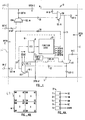
- Fig. 1 there is illustrated in simplified, block diagram form a cell, designated generally with the reference numeral 10, constructed in accordance with the teachings of the present invention.
- the cell 10 is rectangular in shape, having four boundaries labeled North (N), West (W), South (S), and East (E).
- N, W, S and E are 2-to-1 multiplexers 12N, 12W, 12S, and 12E, respectively.
- Each of the IN and OUT busses of the cell 10 connect to a corresponding OUT and IN bus of an adjacent cell.
- the cell 10W partially indicated in phantom on the boundary E of cell 10 has its corresponding output and input busses (located at what would be boundary E of the cell 10W), OUT-E' and IN-E' respectively connected to the IN-W and OUT-W busses of the cell 10. That is, the OUT and IN buses of a cell correspond to the IN and OUT buses, respectively, of a neighbour cell at any one boundary.
- the IN and OUT busses can be structured to convey information in bit-serial format or multi-bit format.
- the advantages of the present invention permit information to be conveyed in parallel, multi-bit format and, therefore, this format is preferred to the bit-serial transfer of information.
- the input and output busses associated with each of the boundaries N, ..., E are coupled to a corresponding one of the inputs of the multiplexer 12 associated with that boundary.
- the input and output busses IN-W and OUT-W associated with boundary W connect to corresponding inputs of the multiplexer 12W also associated with the boundary
- Fig. 1 further illustrates, the outputs of the multiplexers associated with three of the cell boundaries (W, N and E) connect directly to the output bus of an adjacent boundary and, therefore, to one of the inputs of the multiplexer 12 associated with that adjacent boundary.
- the remaining multiplexer output here multiplexer 12S, connects to the output bus OUT-W via a logic circuit 16, which is shown as including a pipeline register configuration 18, function logic 20, and configuration logic 22.
- the output of the multiplexer 12S is communicated to an input of the pipeline register configuration 18, from there to function logic 20.
- the output of the function logic 20 is then coupled to the output bus OUT-W of the boundary W and, as a consequence, to an input of the multiplexer 12W associated with the boundary W.
- the function logic 20 contains the logic function or functions to be implemented by the particular cell.
- function logic 20 could take the form of an arithmetic logic unit, a memory device of particular configuration, certain other digital functions, or a combination of any of the foregoing.
- the configuration logic 22 operates to control the multiplexers 12 via selection signals SEL-W, SEL-S, SEL-E and SEL-N.
- the configuration logic 22 contains power-on reset circuitry (Fig. 6) of generally conventional design that operates to place the cell 10 in a "closed" state in which the selection signals (SEL) cause the multiplexers 12 to de-select all IN busses. In effect, there is an internal loop formed within the cell 10 by selecting, as inputs to the multiplexers 12, the associated output (OUT) busses.
- the multiplexer 12N communicates the output bus OUT-N to the output bus OUT-E; the multiplexer 12E communicates the output bus OUT-E to the output bus OUT-S, and so on.
- the configuration logic 22 also generates four OPEN signals (OPEN-N, E, S, W) that are respectively communicated to the configuration logic of the neighbor cells and the boundaries N, E, S and W of cell 10; and, correspondingly, the neighbor cells each communicate an OPEN signal to the configuration logic 22 of cell 10.
- the OPEN signal from any cell adjacent the boundaries N, ... E, of cell 10 when asserted, operates to cause the multiplexer associated with that boundary to select the corresponding input (IN) bus.
- the cell asserting the OPEN signal correspondingly causes its multiplexer associated with the intervening boundary to select the OUT bus of the cell receiving the OPEN signal.
- the configuration logic 22 will, in turn, assert the SEL-S signal to cause the multiplexer 12S to select the input bus IN-S.
- the cell asserting the OPEN-N' signal will cause its multiplexer (not shown) associated with its boundary N (boundary S for cell 10) to select as an input the OUT-S bus of cell 10; that is, the boundary is "opened” both ways between the two cells.
- FIG. 6 illustrates those portions of cell 10. and the cell at its west (W) boundary, here cell 10(W), involved in opening the boundary to one another.
- W west
- Those elements that have already been described in connection with the discussion of Fig. 1 will keep the designations used in that discussion.
- cell 10 includes a latch 22W, contained in the configuration logic 22, that when set asserts the OPEN-W signal communicated to the cell 10(W).
- latch 22W contained in the configuration logic 22, that when set asserts the OPEN-W signal communicated to the cell 10(W).
- the OPEN-W signal is coupled to one input of a two-input OR gate 23 on its way to the cell 10(W), where it is applied to another input of a two-input OR gate 23'.
- the OPEN-E from the cell 10(W) emanates from a latch 22W', is coupled to the other input of the OR gate 23' and to the other input of the OR gate 23 of cell 10.
- the IN-W bus of cell 10 connects to the OUT-E' bus from cell 10(W), and that the OUT-W bus from cell 10 connects to the IN-E' bus of cell 10(W).
- the cell 10 asserts the OPEN-W signal, to open the boundary W into the cell 10(W), by setting the latch 22W.
- the OPEN-W signal then operates through the medium of the OR gates 23 and 23' to respectively cause the associated (with the boundary in question) multiplexer 12(W),12W to select their corresponding IN-W and IN-E' (i.e OUT-W of cell 10) busses.
- a path of communication is thereby formed from cell 10 to cell 10(W) (via the OUT-W bus and through the multiplexer 12(W)), and likewise from cell 10(W) to cell 10 (via the OUT-E′ and IN-W busses, and through the multiplexer 12W.
- a power-on reset circuit 27W and 27W′ carried by each of the cells 10 and 10(W), respectively.
- the power-on reset circuits 27W, 27W′ are contained in the configuration logic 22, and function, at the time power is applied to the cell, to reset various latches.
- One such latch is the latch 22W, 22W′.
- the power-on reset circuits 27W, 27W′ whose outputs connect to the reset (R) inputs of the latches 22W, 22W′, respectively, operate to reset the latches.
- the associated multiplexers 12W, 12W′ have the inputs connected to the IN-W and IN-W′ busses de-selected in favor of the remaining inputs, thereby placing the cell in its closed state.
- multiplexers 12N, 12E, and 12S (Fig. 1) also have circuitry essentially the same as that shown in Fig. 6; i.e, each would have its selection input coupled to receive the output of an OR gate receiving OPEN signals from a latch (not shown, but substantially the same as latch 22W) of cell 10 and the cell at the associated boundary N, E, and S.
- the output of the power-on circuit 27W would be connected to the reset inputs of such latches (not shown) as connected to latch 22W.
- OPEN signals generated by the cells at the E, N, and W boundaries of cell 10 are also communicated to the configuration logic, where they are received by OR gates (not shown) similar to the OR gate 23 (Fig. 6), for performing similar operations on the associated multiplexers 12 when asserted.
- the bus structure of the IN and OUT busses including those that may be termed an "internal bus" (i.e., bus lines 30, 31, 32, 33 and 34) of the cell 10, may be single-bit or wide.
- the bus structure multi-bit consists of multiple signal lines, so that multi-bit data and control signals can be communicated in parallel with a clock signal.
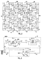
- Fig. 1 The basic architecture presented in Fig. 1 is preferably used to form an array of identical configurations of the cell 10. Each cell, however, is oriented so that it is rotated 180 degrees relative to any neighbor cell. This concept is illustrated in Fig. 2, which shows a three by four array 38 of cells 10 (10A, ..., 10L). The cells 10 are illustrated in more simplified configuration than that of Fig. 1 for the sake of clarity.
- each cell is identically structured, along the lines of the circuit shown in Fig. 1.
- each of the cells 10I, 10L contain four multiplexers 12' and function logic L.
- Fig. 2 is presented to illustrate two important aspects of the invention.
- the first is that when cells are constructed in accordance with the teachings of the present invention to form an array of such cells, there is a preferred orientation of each of the cells, relative to its four principal neighbors (i.e., those neighbors on its north, south, east and west boundaries): Each cell is rotated 180 degrees relative to any adjacent neighbor.
- the multiplexer 12' that drives the function logic L is oriented to be situated in the northeastern corner of the cell.
- each of the neighboring cells 10C, 10H, 10K or 10F has the corresponding multiplexer 12',(i.e., the multiplexer driving the function logic of that cell) rotated 180 degrees relative to the multiplexer orientation of cell 10G .
- the N, E, S and W borders of the cell 10G become, respectively, the borders S, W, N and W when rotated 180 degrees to form any one of the cells adjacent to the cell 10G.
- the cells of such an array 38 as illustrated in Fig. 2 are logically connected to one another by a configuration algorithm to constructs a single signal path that forms a linear array of the cells - such as indicated, for example, by the dotted line 40 in Fig. 2.
- the signal path, or "chain” as it is sometimes called in this art logically connects the function logic L of each of the cells 10 of the chain 40 to one another in serial fashion, using appropriate selection of the multiplexers 12' of each cell. Access to any and all logic circuits 16′ is thereby established, once the chain 40 is formed.
- Fig. 2 Note that the signal path between any function logic L and the next in the chain 40 includes only four multiplexers 12'; no more, and no less.
- This aspect of the invention establishes and makes known the signal delay between any two function logic L in the chain 40: Four multiplexer delays.
- Prior schemes have used multiplexing configurations that could bypass the function logic of any particular cells so that any number of multiplexers could be interposed between two immediately successive function logic circuits, creating the unbounded situation. This required designers to design to a "worst-case" delay condition, creating much slower array operation. With known delay, array operation can be, by design, much faster.
- wafer is meant to refer to a large array of cells 10 formed on the surface of a semiconductor wafer, whether or not that portion is the entire wafer surface.
- the asynchronous approach eliminates the need for a single controlled skew clock, but substitutes a penalty that may be even worse.
- a full handshake between two cells requires waiting a two-way propagation delay between the cells. Also, if the cells have internal clocks, there may be additional delays to synchronize signals to clock edges.
- phase-shifted synchronous clocking similar to that described by F. Manning, "An Approach to Highly Integrated Computer-Maintained Cellular Arrays," IEEE Trans. Comput. , Vol. C- 26, June, 1977, pps. 536-552.
- Phase-shifted synchronous clocking is based on the premise that most communication transfers take place in a single direction, and the clock can be distributed through the same delay and configuration paths as the data. Accordingly, a diagram of a preferred clocking scheme is illustrated in Fig. 3.
- a host computer 50 generates data and clock signals that are communicated to a wafer 52 on an M-bit-wide bus 54.
- the wafer 52 is formed to carry an array of cells (cells 1, ..., N) constructed according to the present invention.
- the clock and data signals are applied to the multiplexer 12'' of the first cell of the array, cell 1, and applied to the function logic 16'' of that cell.
- the data from the function logic 16'' is coupled to a multiplexer 12'' of that cell 1, and selected, along with the clock signal, for communication through the remaining N-1 cells of the wafer 52, and returned to the host system 50 via the return bus 56.
- the data is applied to an input register 60, clocked by the clock signal that accompanied the data.
- the output of the register 60 is applied to a synchronizing register (or registers) 62, clocked by the clock signal (CLOCK) that is applied to the wafer 52 by the input bus 54.
- CLOCK clock signal
- the clock signal therefore, takes the same path through the array of N cells formed on the wafer 52 as that of the data signals.
- the clock is successively delayed at each cell, thereby acquiring a phase shift, relative to the clock at the output of the host 50, that is equal to the delay through the multiplexers 12''.
- the registers 60 and 62 are used to resynchronize the clocks for receiving data by the host system 50 in conventional fashion.
- the only potential problem in this scheme is that the clock pulse width may shrink or grow slightly at each stage if the rise and fall times of the buffers are not identical.
- a simple solution to the problem is to make the clock multiplexer/buffers inverting. Since there are always four multiplexers between cells, the clock arrives without inversion, and asymmetries in rise and fall times at one cell are cancelled out by the next.
- the minimum clock period is governed by: (1) t c ⁇ t r + t e + t SKEW + N ⁇ TMUX MAX where t r is the delay time of the (pipeline) register 18 (Fig. 1), t1 is the delay of the function logic 20, t SKEW is the clock skew, and N ⁇ t and N ⁇ tMUX MAX is the time for N cells of delay through the configuration multiplexers 12''.
- t r is the delay time of the (pipeline) register 18 (Fig. 1)
- t1 is the delay of the function logic 20
- t SKEW is the clock skew
- N ⁇ t and N ⁇ tMUX MAX is the time for N cells of delay through the configuration multiplexers 12''.
- the minimum clock period is: (2) t c ⁇ t r + t1 + 4 ⁇ (tMUX MAX - tMUX MIN ). Note that the clock skew term has been eliminated, and the configuration delay has been reduced to four times the time difference between the minimum and maximum paths through the multiplexers. On a large wafer, the savings due to both the skew and the multiplexer delay terms could lead to a significant cycle time improvement.
- a wafer scale integrated array of cells constructed in accordance with the teachings of the present invention can be configured as a single, long chain or linear array, such as that simplistically illustrated in Fig. 2.
- the chain is formed pursuant to an algorithm which initially locates those cells sufficiently operable to be able to pass data (and clock), and logically connects them in a chain.
- the algorithm proceeds, on a cell-by-cell basis, along the following lines:
- the algorithm continues until the chain returns to the cell at the periphery of the wafer serving as the input/output of that wafer.
- the data path chain formed by the algorithm is illustrated as the dotted line 40. It enters the wafer at the cell 10J, and proceeds sequentially through the cells 10I, 10E back through 10J, and continues through cells 10G, 10B, ..., 10K, returning to the cell 10J where it is taken from the wafer of our example.
- the test performed by the algorithm may be limited, as referred to above, to determining whether the cell has the data-communicating ability (i.e., workable multiplexers and data paths) to be included in the chain. Once the chain is formed, a second testing procedure can be made to determine the operability of the other logic circuitry (e.g., the pipeline registers 18 and function logic 20). Alternatively, the initial cell test could be to determine the working condition of the entire cell.
- Fig. 1 Contained in the configuration logic 22 (Fig. 1) are various registers and latches that are set or reset to indicate various operating states, modes of operation, etc.
- One such bank of latches is illustrated in Fig. 4A at 70, comprising individual latches 71-75.
- the information provided by these latches 71-75 is as follows: The stage 75, when set, results in assertion of the CHAIN signal to indicate that the particular cell is a part of the chain. A cell is not opened if this signal is asserted.
- each cell When each cell is opened, tested, and found to be operable, it forms the head of the developing chain, signified by a "token" being "advanced”(e.g., moved) into that newly tested cell by setting one of the latches 71-74.
- the token indicates which border of the cell brought the chain in, and also indicates the border to be checked for progression of the chain into a neighbor (i.e., the adjacent border, in a clockwise direction, from the entry border).
- the signals SE, SW, NW and NE are mutually exclusive in that only one, if any at all, is asserted at any one time.
- the asserted signal will indicate the particular corner of the cell that is (1) bordered by the boundary crossed by the chain for ingress to the cell and (2) the first boundary to be checked for the next cell selected for progression of the chain. These latches are cleared by the power-up circuit (not shown) contained in the configuration logic 22 (Fig. 1).
- Advancing the token does not necessarily mean that the chain, as it is constructed, will always proceed from a newly-tested cell into an untested cell. Rather, the token could well be advanced into an already tested cell, such as indicated in Fig. 2 where path 40 is shown beginning at cell 10J, proceeding through cell, 10I and into cell 10E.
- Cell 10E is, however, bounded by the wafer periphery, and two inoperable cells 10A and 10F (so indicated by the Xs drawn thereacross in phantom).
- the algorithm checks first to see if the "target" cell (i.e., the cell next in line for possible inclusion in the chain) is, in fact already a part of the chain, and if the boundary between them (the target cell and the newly tested cell, presently holding the token) is open (when a boundary is opened, it is opened both ways). If so, the token is advanced into the target cell, even though it is already in the chain. This is the case shown in Fig. 2, where the path 40 returns from the cell 10E to cell 10I, and from there to cell 10J. There are other instances of this concept shown in Fig. 2.
- the configuration algorithm proceeds along the following lines:
- the wafer is powered-up (i.e, power applied), causing the bank of latches 70 of each of the cells 10 carried by the wafer to be reset; thereby, the signals SE, SW, NW, NE, and CHAIN are deasserted.
- the algorithm next proceeds to the step 80, where a periphery cell is selected by the host computer 50 running the algorithm.
- the cell ("target") is opened by assertion of an OPEN signal associated with the particular boundary, causing the corresponding multiplexer 12 to select as an input the IN bus associated with that boundary.
- step 81 the cell is tested. If it is found to be operable, the algorithm advances to step 83. If, on the other hand, the cell is defective in some way, step 81 is followed by step 82, where a determination is made as to whether the just failed cell is the last peripheral cell of the wafer tested. If not, steps 80 and 81 are repeated until a workable cell is found. If no workable cell can be found at the periphery of the wafer, the wafer is determined to be bad, and the algorithm ends.
- step 83 of the algorithm is performed:
- the "token" is advanced into that cell by setting the one of the latches 71 - 74 (Fig. 4A), corresponding to the cell's boundary entered, and signifying that the cell is now included in the chain by setting latch 75 to assert the CHAIN signal.
- Fig. 4B which can be thought of as showing a portion 68 of a larger wafer, consisting of four cells A, B, C, and D, each structured in accordance with the teachings of the present invention, and oriented as discussed with respect to Fig. 2 (i.e., each cell is rotated 180 degrees relative to any neighboring cell).
- the cell D has just been entered, tested, and found to be in working order by the steps 80 and 81.
- the token is advanced into the cell by setting the latch 73 to assert the NW signal, signifying that the chain being formed entered the boundary (here, W) counterclockwise adjacent to the NW corner of the cell D.
- the NW signal also signifies the next target cell: The cell adjacent the boundary is immediately clockwise from the NW corner.
- the algorithm then sets the latch 75, to identify the cell D as now being part of the chain.
- step 84 a check is made to determine if the chain has progressed back to the host computer 50. If so, the algorithm is exited. If not, step 85 is performed to see if the next cell nominated for inclusion into the chain is, in fact, already in the chain (as indicated by the target cell's asserted CHAIN signal). For example referring again to Fig. 4B, as indicated above, the target cell of the chain is now cell C. before the OPEN signal into cell C is asserted, there is a check to determine if cell C's CHAIN signal is asserted. If so, and that border has previously been opened, step 85 is followed by step 83, and the token is advanced (setting the appropriate one of the latches 71 - 74 of the target cell).
- step 83 the token is advanced to the next one of the latches 71 - 75 of the cell D to identify the next boundary corner in order, NE.
- latch 73 is cleared and latch 74 set.
- the cell on the boundary clockwise adjacent the NE corner of the cell, cell A, is the new target cell.
- step 85 the algorithm proceeds from step 85 to step 86 to open the target cell, cell C, by asserting the OPEN signal into the cell.
- the OPEN signal causes the configuration logic 22 to operate the multiplexer 12 of cell C associated with the boundary between cells D and C to select the IN bus from cell D (Fig. 1).
- the algorithm now proceeds to test cell C at step 87. If the test fails, finding cell C to be defective in some way, the OPEN signal to cell C (generated by cell D) is deasserted in step 90, and a return to step 83 is made.
- step 87 is left in favor of a return to step 83, where the token is advanced into cell C by setting the latch boundary just crossed, i.e., latch 72 of that cell, to assert the SW signal, and the CHAIN signal asserted by setting latch 75 of cell C.
- Steps 84 and 85 are performed as described above.
- step 87 we will assume that the cells that are clockwise adjacent the SW and NW boundaries are unable to pass the test performed in step 87.
- steps 84, 85, 86, 87, and 90 will be performed once while latch 72 is set.
- the algorithm returns to step 83 to move the token to assert the NW signal, and steps 84 - 90 again performed, again to find the target inoperable.
- step 87 will proceed back to step 83, and cell B will be included in the chain that is so far formed by cells D, C, and B.
- Fig. 2 illustrates, a return is made to a peripheral cell or the seminal cell (cell D in Fig. 4B, or cell 10J in Fig. 2), at which time the step 84 moves to the exit step, DONE.
- a cell designated generally with the reference numeral 110, is constructed in much the same way as that of Fig. 1, i.e., the cell 110 is provided four edge boundaries, north ..., west (N, ..., W), separating it from its four adjacent neighbors.
- N, ..., W has associated therewith a corresponding one of the four two-input multiplexers 112N, ..., 112W, respectively.
- each of the multiplexers 112N, ..., 112W receives a multi-bit input bus IN-N, ..., IN-W, respectively, from the neighbor cell located at the associated boundary.
- each of the input busses IN-N, ..., IN-W comprises 55 signal lines, carrying 39 bits of data (DATA), 11 bits of address (ADDR), four bits of instruction (INSTR), and a periodic clock (CLOCK) signal.
- Three of the multiplexers, 112N, 112E and 112W couple their respective 55-bit outputs to a second input of the multiplexer associated with a clockwise adjacent boundary.
- the remaining multiplexer, 112S has its 55-bit output coupled to logic circuit 116, where it is received by the input of a pipeline register configuration 118 that is clocked by the CLOCK signal.
- the logic circuit 116 (which corresponds to the logic circuit 16 in Fig. 1) includes, in addition to the pipeline register configuration 118, a dynamic random access memory configuration 140 of conventional design, a decode circuit 142 that is coupled to control logic , 144. Address registers 146 are also included, as is a shift/pass multiplexer 148.
- the signalling produced by the control logic 144 directs operation of the cell in response to various instructions decoded by the decode logic 142.
- the selected one of the latches 33 e.g. 22W, Fig.6
- the configuration latches 122 which in turn, causes another of the selection signals SI-N, ..., SEL-E to be asserted (in addition to the one asserted by the OPEN signal from the neighbour cell that caused the cell to be entered).
- a very high capacity memory architecture can be obtained.
- the DRAM 140 could very well be structured as an N by 39 bit word memory. However, 39 bit words are unusual. Therefor, it is more likely that the DRAM 140 configuration is N by M (N words, each M bits in length). If, however, the word length desired to be used is larger, for example, than M bits, the shift/pass multiplexer 148 can used.
- a number of such cells 110 forming a wafer scale integrated circuit memory have the potential of providing immense storage capacity.
- DRAM 140 is an N by 1 bit RAM, this configuration is best believed implemented by having each addressable (multi-bit) word spread across a number of cells 110.
- the shift/pass multiplexer 148 is used: In memory write operations, the shift/pass multiplexer 148 functions to strip the least significant bit (LSB) of the DATA word presented to that cell 110 for storage in the memory configuration 140. The shift/pass multiplexer 148 then shifts the remainder of the word down (moving the least next least significant bit (LSB + 1) into the LSB position) before it is communicated to the next cell in the chain, where the same operation occurs.
- LSB least significant bit
- the shift/pass multiplexer 148 functions in reverse when involved in a read operation: Access to the memory configuration 140 produces a single bit that is added to a word as it (the word ) passes through the particular cell 110.
- Operation of the cell 110, and the memory function is carries generally is as follows: Parallel, multi-bit information, containing the 39 bits of data (DATA), 11 bits of address (ADDR) and 4 bits of instruction (INSTR), all accompanied by the periodic clock (CLOCK) signal, are applied to a chain formed by a number of cells 110, and sequentially applied to each cell in order.
- DATA 39 bits of data
- ADDR 11 bits of address
- ISTR all accompanied by the periodic clock
- the information enters the pipeline register 118, and from there coupled to the memory system of function logic 120.
- the instructions, INSTR e.g., read, write, etc.
- ADDR address indicating the memory location to be accessed for a read or write operation
- Control logic 144 then operates to perform the access of the DRAM 140.
- data appearing at the data input (DI) of the DRAM 140 is write to the specified memory location; and in the case of a read, the accessed data is coupled from the data output (DO) of the DRAM 140 to the output bus of the cell 110, OUT-W, via the signal lines 134.
- the output of the logic circuit 116 will be communicated directly to the OUT-W output bus, as well as being conducted to the output busses OUT-W, N, E by the multiplexers 112W, 112N, or 112E, respectively.
- the cell next in order in the chain will be configured to have one of its multiplexers 112 set to select the connection to the output bus of this cell 110.
- the address register structure 146 is used for configuring the address base of the DRAM 140 of the cell 110, relative to DRAMs that may be contained in other cells of a wafer-scale integrated array of cells 110 as described hereinabove.
- Address registers 146 may be set to specify the address boundaries of the address space implemented by the DRAM 140. Addresses for a read or write operation that are within this address space will cause the address register 146 to enable the control logic 144 to cause access of the DRAM 140. Conversely, addresses that are not within the address space specified by the address registers 146 will not be able to access the DRAM 140 of the particular cell 110. (Although another of the cells 110 in the hypothetical array will have this address within its address space specified by the address registers 146.)
- the configuration latches 71-75 can be replaced with fuses that perform the sample function, with the cells being tested by probed connections from the host, and the fused connections interrupted as a result of the test to configure each cell in the chain.
- the foregoing discussion has referred to an array of identically constructed cells, this need not be true to practice the present invention.
- certain of the cells 10 may carry memory as the logic function 20, while others may carry arithmetic logic units, or other digital function.
- the configuration may be made the subject of a number of modifications and variations. When a cell is entered during formation of the chain, all boundaries of that cell could be opened, and the first of the open boundaries found to separate that cell from another target cell becomes the one across which the token is advanced.
Landscapes
- Physics & Mathematics (AREA)
- Engineering & Computer Science (AREA)
- Computer Hardware Design (AREA)
- Computing Systems (AREA)
- General Engineering & Computer Science (AREA)
- Mathematical Physics (AREA)
- Design And Manufacture Of Integrated Circuits (AREA)
- Logic Circuits (AREA)
- Semiconductor Integrated Circuits (AREA)
Claims (9)
- Cellule logique (10) appropriée pour une utilisation dans un réseau cellulaire, la cellule logique étant réalisée de manière à avoir N limites (Nord, Sud, Est, Ouest), chaque limite ayant des moyens de bus d'entrée et de sortie (IN-N/OUT-N, IN-S/OUT-S, IN-E/OUT-E, IN-W/OUT-W) pour communiquer respectivement des signaux, chaque limite étant située entre une première et une seconde limites adjacentes, la cellule logique comprenant :des moyens de sélection (12N, 12S, 12E, 12W) associés à chaque limite et ayant une pluralité d'entrées de sélection, couplées pour recevoir le moyen de bus d'entrée et le moyen de bus de sortie de la limite associée, et une sortie de sélection (30, 31, 32, 33), la sortie de sélection associée à N-1 des limites (Ouest, Nord, Est) étant couplée au moyen de bus de sortie (OVIN, OUT-E, OUT-S) de la première limite adjacente correspondante (Nord, Est, Sud), les moyens de sélection étant aptes à fonctionner pour effectuer une sélection entre les moyens de bus d'entrée et les moyens de bus de sortie (IN-W/OUT-W, IN-N/OUT-N, IN-E/OUT-E) ;des moyens logiques (16, 18, 20) couplés entre la sortie de sélection (33) du moyen de sélection restant (12S) et le moyen de bus de sortie (OUT-W) de la première limite adjacente correspondante (Ouest), les moyens logiques étant configurés et construits pour exécuter des fonctions logiques ; etdes moyens de commande (22) couplés de manière fonctionnelle à chacun des moyens de sélection pour provoquer, au niveau de chaque moyen de sélection, la sélection d'une entrée de la pluralité d'entrées de sélection.
- Cellule logique de la revendication 1, les moyens de commande comprenant des moyens de mise sous tension (27W, 27W') pouvant être actionnés pour amener chacun des moyens de sélection à sélectionner le moyen de bus de sortie correspondant pour communication avec la sortie de sélection.
- Cellule logique de la revendication 1 ou 2, comprenant des signaux OPEN (OUVRIR) (OPEN-N, OPEN-S, OPEN-E, OPEN-W) associés à chacune des limites (Nord, Sud, Est, Ouest), et des moyens sensibles à la déclaration de l'un quelconque des signaux OPEN pour amener les moyens de sélection correspondants associés à cette limite à sélectionner le moyen de bus d'entrée pour communication avec la sortie de sélection.
- En combinaison, une pluralité de dites cellules logiques (10A, 10B, ..., 10L) selon la revendication 1, 2 ou 3 de construction essentiellement identiques et réalisées sur une plaquette de semiconducteur.
- La combinaison de la revendication 4, dans laquelle chacune des cellules logiques est orientée de manière à être tournée de 180° par rapport à une cellule logique adjacente quelconque.
- La combinaison de la revendication 4 ou 5, comprenant des signaux OPEN (OUVRIR) (OPEN-N, ..., OPEN-W) associés aux limites de chacune des cellules logiques, et des moyens sensibles à la déclaration de l'un quelconque des signaux OPEN pour amener les moyens de sélection correspondants à sélectionner le moyen de bus d'entrée pour communication avec la sortie de sélection.
- La combinaison de la revendication 6, dans laquelle chacune des cellules logiques comprend des moyens (22) pour générer les signaux OPEN (OUVRIR), et des moyens pour communiquer les signaux OPEN générés à chaque cellule logique adjacente.
- La combinaison de l'une quelconque des revendications 4 à 7, comprenant des moyens (12N, 12(S), ..., 12W, 12 (W)) pour connecter de manière logique certaines des cellules logiques dans un réseau linéaire pour communiquer les données le long de ce réseau.
- La combinaison de la revendication 8 dans laquelle la connexion logique du réseau linéaire incorpore l'utilisation des moyens de sélection (12(N), 12 (S), 12 (E), 12 (W)) des cellules logiques adjacentes du réseau.
Applications Claiming Priority (2)
| Application Number | Priority Date | Filing Date | Title |
|---|---|---|---|
| US07/346,203 US5203005A (en) | 1989-05-02 | 1989-05-02 | Cell structure for linear array wafer scale integration architecture with capability to open boundary i/o bus without neighbor acknowledgement |
| US346203 | 1999-07-01 |
Publications (3)
| Publication Number | Publication Date |
|---|---|
| EP0398552A2 EP0398552A2 (fr) | 1990-11-22 |
| EP0398552A3 EP0398552A3 (fr) | 1992-03-25 |
| EP0398552B1 true EP0398552B1 (fr) | 1996-03-13 |
Family
ID=23358389
Family Applications (1)
| Application Number | Title | Priority Date | Filing Date |
|---|---|---|---|
| EP90304801A Expired - Lifetime EP0398552B1 (fr) | 1989-05-02 | 1990-05-02 | Architecture d'intégration à l'échelle de la plaquette pour un réseau à interconnexion linéaire |
Country Status (6)
| Country | Link |
|---|---|
| US (2) | US5203005A (fr) |
| EP (1) | EP0398552B1 (fr) |
| JP (1) | JPH0369138A (fr) |
| AU (1) | AU638454B2 (fr) |
| CA (1) | CA2015853A1 (fr) |
| DE (1) | DE69025795T2 (fr) |
Cited By (27)
| Publication number | Priority date | Publication date | Assignee | Title |
|---|---|---|---|---|
| US7394284B2 (en) | 2002-09-06 | 2008-07-01 | Pact Xpp Technologies Ag | Reconfigurable sequencer structure |
| US7434191B2 (en) | 2001-09-03 | 2008-10-07 | Pact Xpp Technologies Ag | Router |
| US7565525B2 (en) | 1996-12-09 | 2009-07-21 | Pact Xpp Technologies Ag | Runtime configurable arithmetic and logic cell |
| US7577822B2 (en) | 2001-12-14 | 2009-08-18 | Pact Xpp Technologies Ag | Parallel task operation in processor and reconfigurable coprocessor configured based on information in link list including termination information for synchronization |
| US7595659B2 (en) | 2000-10-09 | 2009-09-29 | Pact Xpp Technologies Ag | Logic cell array and bus system |
| US7650448B2 (en) | 1996-12-20 | 2010-01-19 | Pact Xpp Technologies Ag | I/O and memory bus system for DFPS and units with two- or multi-dimensional programmable cell architectures |
| US7657861B2 (en) | 2002-08-07 | 2010-02-02 | Pact Xpp Technologies Ag | Method and device for processing data |
| US7657877B2 (en) | 2001-06-20 | 2010-02-02 | Pact Xpp Technologies Ag | Method for processing data |
| US7822881B2 (en) | 1996-12-27 | 2010-10-26 | Martin Vorbach | Process for automatic dynamic reloading of data flow processors (DFPs) and units with two- or three-dimensional programmable cell architectures (FPGAs, DPGAs, and the like) |
| US7840842B2 (en) | 2001-09-03 | 2010-11-23 | Martin Vorbach | Method for debugging reconfigurable architectures |
| US7844796B2 (en) | 2001-03-05 | 2010-11-30 | Martin Vorbach | Data processing device and method |
| US7996827B2 (en) | 2001-08-16 | 2011-08-09 | Martin Vorbach | Method for the translation of programs for reconfigurable architectures |
| US8058899B2 (en) | 2000-10-06 | 2011-11-15 | Martin Vorbach | Logic cell array and bus system |
| US8099618B2 (en) | 2001-03-05 | 2012-01-17 | Martin Vorbach | Methods and devices for treating and processing data |
| US8127061B2 (en) | 2002-02-18 | 2012-02-28 | Martin Vorbach | Bus systems and reconfiguration methods |
| US8156284B2 (en) | 2002-08-07 | 2012-04-10 | Martin Vorbach | Data processing method and device |
| US8230411B1 (en) | 1999-06-10 | 2012-07-24 | Martin Vorbach | Method for interleaving a program over a plurality of cells |
| US8250503B2 (en) | 2006-01-18 | 2012-08-21 | Martin Vorbach | Hardware definition method including determining whether to implement a function as hardware or software |
| US8281108B2 (en) | 2002-01-19 | 2012-10-02 | Martin Vorbach | Reconfigurable general purpose processor having time restricted configurations |
| US8301872B2 (en) | 2000-06-13 | 2012-10-30 | Martin Vorbach | Pipeline configuration protocol and configuration unit communication |
| USRE44365E1 (en) | 1997-02-08 | 2013-07-09 | Martin Vorbach | Method of self-synchronization of configurable elements of a programmable module |
| US8686475B2 (en) | 2001-09-19 | 2014-04-01 | Pact Xpp Technologies Ag | Reconfigurable elements |
| US8686549B2 (en) | 2001-09-03 | 2014-04-01 | Martin Vorbach | Reconfigurable elements |
| US8812820B2 (en) | 2003-08-28 | 2014-08-19 | Pact Xpp Technologies Ag | Data processing device and method |
| US8819505B2 (en) | 1997-12-22 | 2014-08-26 | Pact Xpp Technologies Ag | Data processor having disabled cores |
| US8914590B2 (en) | 2002-08-07 | 2014-12-16 | Pact Xpp Technologies Ag | Data processing method and device |
| US9037807B2 (en) | 2001-03-05 | 2015-05-19 | Pact Xpp Technologies Ag | Processor arrangement on a chip including data processing, memory, and interface elements |
Families Citing this family (57)
| Publication number | Priority date | Publication date | Assignee | Title |
|---|---|---|---|---|
| US5231588A (en) * | 1989-08-15 | 1993-07-27 | Advanced Micro Devices, Inc. | Programmable gate array with logic cells having symmetrical input/output structures |
| US5212652A (en) * | 1989-08-15 | 1993-05-18 | Advanced Micro Devices, Inc. | Programmable gate array with improved interconnect structure |
| US5644496A (en) * | 1989-08-15 | 1997-07-01 | Advanced Micro Devices, Inc. | Programmable logic device with internal time-constant multiplexing of signals from external interconnect buses |
| US5315130A (en) * | 1990-03-30 | 1994-05-24 | Tactical Fabs, Inc. | Very high density wafer scale device architecture |
| JPH05181816A (ja) * | 1992-01-07 | 1993-07-23 | Hitachi Ltd | 並列データ処理装置及びマイクロプロセッサ |
| JPH05235782A (ja) * | 1992-02-19 | 1993-09-10 | Fujitsu Ltd | 垂直データ・水平データ交換方法及び回路 |
| JP3244936B2 (ja) * | 1993-04-26 | 2002-01-07 | 財団法人工業技術研究院 | ファジイ論理メンバーシップ関数を生成する装置及び方法 |
| US6154053A (en) * | 1993-09-02 | 2000-11-28 | Xilinx, Inc. | Look-ahead carry structure with homogeneous CLB structure and pitch larger than CLB pitch |
| US5546018A (en) * | 1993-09-02 | 1996-08-13 | Xilinx, Inc. | Fast carry structure with synchronous input |
| US5481206A (en) * | 1993-09-02 | 1996-01-02 | Xilinx, Inc. | Circuit for fast carry and logic |
| US6288570B1 (en) | 1993-09-02 | 2001-09-11 | Xilinx, Inc. | Logic structure and circuit for fast carry |
| US5898319A (en) * | 1993-09-02 | 1999-04-27 | Xilinx, Inc. | Method and structure for providing fast conditional sum in a field programmable gate array |
| US5629886A (en) * | 1993-09-02 | 1997-05-13 | Xilinx, Inc. | Method and structure for providing fast propagation of a carry signal in a field programmable gate array |
| JP2746093B2 (ja) * | 1993-12-30 | 1998-04-28 | 日本電気株式会社 | 半導体装置 |
| EP1046994A3 (fr) * | 1994-03-22 | 2000-12-06 | Hyperchip Inc. | Architecture d'insensibilité aux défaillances, à remplacement direct et efficace de cellules , supportant des systèmes totalement intégrés ainsi que des dispositifs de communication directs avec l'opérateur du système |
| US6028446A (en) * | 1995-06-06 | 2000-02-22 | Advanced Micro Devices, Inc. | Flexible synchronous and asynchronous circuits for a very high density programmable logic device |
| KR0147706B1 (ko) * | 1995-06-30 | 1998-09-15 | 김주용 | 고속 동기형 마스크 롬 |
| US5692165A (en) * | 1995-09-12 | 1997-11-25 | Micron Electronics Inc. | Memory controller with low skew control signal |
| US5943242A (en) | 1995-11-17 | 1999-08-24 | Pact Gmbh | Dynamically reconfigurable data processing system |
| DE19654593A1 (de) * | 1996-12-20 | 1998-07-02 | Pact Inf Tech Gmbh | Umkonfigurierungs-Verfahren für programmierbare Bausteine zur Laufzeit |
| US6338106B1 (en) | 1996-12-20 | 2002-01-08 | Pact Gmbh | I/O and memory bus system for DFPS and units with two or multi-dimensional programmable cell architectures |
| DE19654846A1 (de) * | 1996-12-27 | 1998-07-09 | Pact Inf Tech Gmbh | Verfahren zum selbständigen dynamischen Umladen von Datenflußprozessoren (DFPs) sowie Bausteinen mit zwei- oder mehrdimensionalen programmierbaren Zellstrukturen (FPGAs, DPGAs, o. dgl.) |
| DE19704044A1 (de) * | 1997-02-04 | 1998-08-13 | Pact Inf Tech Gmbh | Verfahren zur automatischen Adressgenerierung von Bausteinen innerhalb Clustern aus einer Vielzahl dieser Bausteine |
| DE19704728A1 (de) | 1997-02-08 | 1998-08-13 | Pact Inf Tech Gmbh | Verfahren zur Selbstsynchronisation von konfigurierbaren Elementen eines programmierbaren Bausteines |
| DE19704742A1 (de) * | 1997-02-11 | 1998-09-24 | Pact Inf Tech Gmbh | Internes Bussystem für DFPs, sowie Bausteinen mit zwei- oder mehrdimensionalen programmierbaren Zellstrukturen, zur Bewältigung großer Datenmengen mit hohem Vernetzungsaufwand |
| US6789212B1 (en) * | 1997-04-24 | 2004-09-07 | Edwin E. Klingman | Basic cell for N-dimensional self-healing arrays |
| DE19807872A1 (de) | 1998-02-25 | 1999-08-26 | Pact Inf Tech Gmbh | Verfahren zur Verwaltung von Konfigurationsdaten in Datenflußprozessoren sowie Bausteinen mit zwei- oder mehrdimensionalen programmierbaren Zellstruktur (FPGAs, DPGAs, o. dgl. |
| US6294926B1 (en) * | 1999-07-16 | 2001-09-25 | Philips Electronics North America Corporation | Very fine-grain field programmable gate array architecture and circuitry |
| IT1313346B1 (it) * | 1999-09-06 | 2002-07-23 | Abb Ricerca Spa | Metodo per eseguire la programmazione fuori linea di un robotindustriale. |
| US6671837B1 (en) * | 2000-06-06 | 2003-12-30 | Intel Corporation | Device and method to test on-chip memory in a production environment |
| US20040015899A1 (en) * | 2000-10-06 | 2004-01-22 | Frank May | Method for processing data |
| US6990555B2 (en) | 2001-01-09 | 2006-01-24 | Pact Xpp Technologies Ag | Method of hierarchical caching of configuration data having dataflow processors and modules having two- or multidimensional programmable cell structure (FPGAs, DPGAs, etc.) |
| US20090210653A1 (en) * | 2001-03-05 | 2009-08-20 | Pact Xpp Technologies Ag | Method and device for treating and processing data |
| US7210129B2 (en) | 2001-08-16 | 2007-04-24 | Pact Xpp Technologies Ag | Method for translating programs for reconfigurable architectures |
| US20090300262A1 (en) * | 2001-03-05 | 2009-12-03 | Martin Vorbach | Methods and devices for treating and/or processing data |
| US7581076B2 (en) | 2001-03-05 | 2009-08-25 | Pact Xpp Technologies Ag | Methods and devices for treating and/or processing data |
| EP1470478A2 (fr) * | 2002-01-18 | 2004-10-27 | PACT XPP Technologies AG | Procede de compilation |
| US6667561B2 (en) * | 2002-03-13 | 2003-12-23 | Globespanvirata, Incorporated | Integrated circuit capable of operating in multiple orientations |
| US20060075211A1 (en) * | 2002-03-21 | 2006-04-06 | Martin Vorbach | Method and device for data processing |
| US20040012244A1 (en) * | 2002-07-17 | 2004-01-22 | Waterman Terry M. | Device to protect vehicle wheels and axles from debris |
| US20110238948A1 (en) * | 2002-08-07 | 2011-09-29 | Martin Vorbach | Method and device for coupling a data processing unit and a data processing array |
| US20060001669A1 (en) | 2002-12-02 | 2006-01-05 | Sehat Sutardja | Self-reparable semiconductor and method thereof |
| US7340644B2 (en) | 2002-12-02 | 2008-03-04 | Marvell World Trade Ltd. | Self-reparable semiconductor and method thereof |
| US7185225B2 (en) | 2002-12-02 | 2007-02-27 | Marvell World Trade Ltd. | Self-reparable semiconductor and method thereof |
| DE112004000026D2 (de) * | 2003-04-04 | 2006-06-14 | Pact Xpp Technologies Ag | Verfahren und Vorrichtung für die Datenverarbeitung |
| ITTO20040415A1 (it) * | 2004-06-22 | 2004-09-22 | St Microelectronics Srl | Architettura di processore multidimensionale |
| US7831804B2 (en) * | 2004-06-22 | 2010-11-09 | St Microelectronics S.R.L. | Multidimensional processor architecture |
| US20090031104A1 (en) * | 2005-02-07 | 2009-01-29 | Martin Vorbach | Low Latency Massive Parallel Data Processing Device |
| US7478222B2 (en) * | 2005-03-29 | 2009-01-13 | Karl M. Fant | Programmable pipeline array |
| US7281942B2 (en) * | 2005-11-18 | 2007-10-16 | Ideal Industries, Inc. | Releasable wire connector |
| US7693257B2 (en) | 2006-06-29 | 2010-04-06 | Accuray Incorporated | Treatment delivery optimization |
| WO2010037201A1 (fr) * | 2008-09-30 | 2010-04-08 | Wicksoft Corporation | Système et procédé permettant une gestion sécurisée d'un accès utilisateur mobile à des ressources de réseau d'entreprise |
| US8798579B2 (en) | 2008-09-30 | 2014-08-05 | Xe2 Ltd. | System and method for secure management of mobile user access to network resources |
| JP2011123612A (ja) * | 2009-12-09 | 2011-06-23 | Sanyo Electric Co Ltd | メモリ制御装置 |
| JP5711889B2 (ja) * | 2010-01-27 | 2015-05-07 | スパンション エルエルシー | リコンフィギュラブル回路および半導体集積回路 |
| US8718079B1 (en) | 2010-06-07 | 2014-05-06 | Marvell International Ltd. | Physical layer devices for network switches |
| US10964682B2 (en) * | 2016-09-30 | 2021-03-30 | Intel Corporation | Data storage system using wafer-level packaging |
Family Cites Families (18)
| Publication number | Priority date | Publication date | Assignee | Title |
|---|---|---|---|---|
| GB1377859A (en) * | 1972-08-03 | 1974-12-18 | Catt I | Digital integrated circuits |
| US4038648A (en) * | 1974-06-03 | 1977-07-26 | Chesley Gilman D | Self-configurable circuit structure for achieving wafer scale integration |
| US4092733A (en) * | 1976-05-07 | 1978-05-30 | Mcdonnell Douglas Corporation | Electrically alterable interconnection |
| GB2082354B (en) * | 1980-08-21 | 1984-04-11 | Burroughs Corp | Improvements in or relating to wafer-scale integrated circuits |
| GB2083929B (en) * | 1980-08-21 | 1984-03-07 | Burroughs Corp | Branched labyrinth wafer scale integrated circuit |
| GB2128381B (en) * | 1980-08-21 | 1984-09-19 | Burroughs Corp | Memory element for a wafer scale integrated circuit |
| GB2089536B (en) * | 1980-12-12 | 1984-05-23 | Burroughs Corp | Improvement in or relating to wafer scale integrated circuits |
| GB2114782B (en) * | 1981-12-02 | 1985-06-05 | Burroughs Corp | Branched-spiral wafer-scale integrated circuit |
| DE3279328D1 (en) * | 1981-12-08 | 1989-02-09 | Unisys Corp | Constant-distance structure polycellular very large scale integrated circuit |
| GB2177825B (en) * | 1985-07-12 | 1989-07-26 | Anamartic Ltd | Control system for chained circuit modules |
| US5072424A (en) * | 1985-07-12 | 1991-12-10 | Anamartic Limited | Wafer-scale integrated circuit memory |
| GB8606695D0 (en) * | 1986-03-18 | 1986-04-23 | Sinclair Res Ltd | Random chip addressing algorithm for wsi |
| US4910665A (en) * | 1986-09-02 | 1990-03-20 | General Electric Company | Distributed processing system including reconfigurable elements |
| US5058001A (en) * | 1987-03-05 | 1991-10-15 | International Business Machines Corporation | Two-dimensional array of processing elements for emulating a multi-dimensional network |
| US4928022A (en) * | 1987-07-17 | 1990-05-22 | Trw Inc. | Redundancy interconnection circuitry |
| US5068823A (en) * | 1988-07-11 | 1991-11-26 | Star Semiconductor Corporation | Programmable integrated circuit using topological and parametric data to selectively connect and configure different high level functional blocks thereof |
| KR900003884A (ko) * | 1988-08-12 | 1990-03-27 | 미다 가쓰시게 | 대규모 반도체 집적회로 장치 |
| US5105425A (en) * | 1989-12-29 | 1992-04-14 | Westinghouse Electric Corp. | Adaptive or fault tolerant full wafer nonvolatile memory |
-
1989
- 1989-05-02 US US07/346,203 patent/US5203005A/en not_active Expired - Lifetime
-
1990
- 1990-05-01 JP JP2115674A patent/JPH0369138A/ja active Pending
- 1990-05-01 CA CA002015853A patent/CA2015853A1/fr not_active Abandoned
- 1990-05-02 AU AU54708/90A patent/AU638454B2/en not_active Ceased
- 1990-05-02 DE DE69025795T patent/DE69025795T2/de not_active Expired - Fee Related
- 1990-05-02 EP EP90304801A patent/EP0398552B1/fr not_active Expired - Lifetime
- 1990-08-22 US US07/570,937 patent/US5287472A/en not_active Expired - Lifetime
Cited By (52)
| Publication number | Priority date | Publication date | Assignee | Title |
|---|---|---|---|---|
| US7565525B2 (en) | 1996-12-09 | 2009-07-21 | Pact Xpp Technologies Ag | Runtime configurable arithmetic and logic cell |
| US8156312B2 (en) | 1996-12-09 | 2012-04-10 | Martin Vorbach | Processor chip for reconfigurable data processing, for processing numeric and logic operations and including function and interconnection control units |
| US7822968B2 (en) | 1996-12-09 | 2010-10-26 | Martin Vorbach | Circuit having a multidimensional structure of configurable cells that include multi-bit-wide inputs and outputs |
| US8195856B2 (en) | 1996-12-20 | 2012-06-05 | Martin Vorbach | I/O and memory bus system for DFPS and units with two- or multi-dimensional programmable cell architectures |
| US7899962B2 (en) | 1996-12-20 | 2011-03-01 | Martin Vorbach | I/O and memory bus system for DFPs and units with two- or multi-dimensional programmable cell architectures |
| US7650448B2 (en) | 1996-12-20 | 2010-01-19 | Pact Xpp Technologies Ag | I/O and memory bus system for DFPS and units with two- or multi-dimensional programmable cell architectures |
| US7822881B2 (en) | 1996-12-27 | 2010-10-26 | Martin Vorbach | Process for automatic dynamic reloading of data flow processors (DFPs) and units with two- or three-dimensional programmable cell architectures (FPGAs, DPGAs, and the like) |
| USRE45223E1 (en) | 1997-02-08 | 2014-10-28 | Pact Xpp Technologies Ag | Method of self-synchronization of configurable elements of a programmable module |
| USRE45109E1 (en) | 1997-02-08 | 2014-09-02 | Pact Xpp Technologies Ag | Method of self-synchronization of configurable elements of a programmable module |
| USRE44365E1 (en) | 1997-02-08 | 2013-07-09 | Martin Vorbach | Method of self-synchronization of configurable elements of a programmable module |
| US8819505B2 (en) | 1997-12-22 | 2014-08-26 | Pact Xpp Technologies Ag | Data processor having disabled cores |
| US8468329B2 (en) | 1999-02-25 | 2013-06-18 | Martin Vorbach | Pipeline configuration protocol and configuration unit communication |
| US8726250B2 (en) | 1999-06-10 | 2014-05-13 | Pact Xpp Technologies Ag | Configurable logic integrated circuit having a multidimensional structure of configurable elements |
| US8312200B2 (en) | 1999-06-10 | 2012-11-13 | Martin Vorbach | Processor chip including a plurality of cache elements connected to a plurality of processor cores |
| US8230411B1 (en) | 1999-06-10 | 2012-07-24 | Martin Vorbach | Method for interleaving a program over a plurality of cells |
| US8301872B2 (en) | 2000-06-13 | 2012-10-30 | Martin Vorbach | Pipeline configuration protocol and configuration unit communication |
| US8471593B2 (en) | 2000-10-06 | 2013-06-25 | Martin Vorbach | Logic cell array and bus system |
| US8058899B2 (en) | 2000-10-06 | 2011-11-15 | Martin Vorbach | Logic cell array and bus system |
| US9047440B2 (en) | 2000-10-06 | 2015-06-02 | Pact Xpp Technologies Ag | Logical cell array and bus system |
| US7595659B2 (en) | 2000-10-09 | 2009-09-29 | Pact Xpp Technologies Ag | Logic cell array and bus system |
| US8099618B2 (en) | 2001-03-05 | 2012-01-17 | Martin Vorbach | Methods and devices for treating and processing data |
| US8145881B2 (en) | 2001-03-05 | 2012-03-27 | Martin Vorbach | Data processing device and method |
| US9075605B2 (en) | 2001-03-05 | 2015-07-07 | Pact Xpp Technologies Ag | Methods and devices for treating and processing data |
| US7844796B2 (en) | 2001-03-05 | 2010-11-30 | Martin Vorbach | Data processing device and method |
| US9037807B2 (en) | 2001-03-05 | 2015-05-19 | Pact Xpp Technologies Ag | Processor arrangement on a chip including data processing, memory, and interface elements |
| US8312301B2 (en) | 2001-03-05 | 2012-11-13 | Martin Vorbach | Methods and devices for treating and processing data |
| US7657877B2 (en) | 2001-06-20 | 2010-02-02 | Pact Xpp Technologies Ag | Method for processing data |
| US7996827B2 (en) | 2001-08-16 | 2011-08-09 | Martin Vorbach | Method for the translation of programs for reconfigurable architectures |
| US8869121B2 (en) | 2001-08-16 | 2014-10-21 | Pact Xpp Technologies Ag | Method for the translation of programs for reconfigurable architectures |
| US8209653B2 (en) | 2001-09-03 | 2012-06-26 | Martin Vorbach | Router |
| US8686549B2 (en) | 2001-09-03 | 2014-04-01 | Martin Vorbach | Reconfigurable elements |
| US7434191B2 (en) | 2001-09-03 | 2008-10-07 | Pact Xpp Technologies Ag | Router |
| US7840842B2 (en) | 2001-09-03 | 2010-11-23 | Martin Vorbach | Method for debugging reconfigurable architectures |
| US8069373B2 (en) | 2001-09-03 | 2011-11-29 | Martin Vorbach | Method for debugging reconfigurable architectures |
| US8407525B2 (en) | 2001-09-03 | 2013-03-26 | Pact Xpp Technologies Ag | Method for debugging reconfigurable architectures |
| US8429385B2 (en) | 2001-09-03 | 2013-04-23 | Martin Vorbach | Device including a field having function cells and information providing cells controlled by the function cells |
| US8686475B2 (en) | 2001-09-19 | 2014-04-01 | Pact Xpp Technologies Ag | Reconfigurable elements |
| US7577822B2 (en) | 2001-12-14 | 2009-08-18 | Pact Xpp Technologies Ag | Parallel task operation in processor and reconfigurable coprocessor configured based on information in link list including termination information for synchronization |
| US8281108B2 (en) | 2002-01-19 | 2012-10-02 | Martin Vorbach | Reconfigurable general purpose processor having time restricted configurations |
| US8127061B2 (en) | 2002-02-18 | 2012-02-28 | Martin Vorbach | Bus systems and reconfiguration methods |
| US8914590B2 (en) | 2002-08-07 | 2014-12-16 | Pact Xpp Technologies Ag | Data processing method and device |
| US7657861B2 (en) | 2002-08-07 | 2010-02-02 | Pact Xpp Technologies Ag | Method and device for processing data |
| US8156284B2 (en) | 2002-08-07 | 2012-04-10 | Martin Vorbach | Data processing method and device |
| US8281265B2 (en) | 2002-08-07 | 2012-10-02 | Martin Vorbach | Method and device for processing data |
| US8803552B2 (en) | 2002-09-06 | 2014-08-12 | Pact Xpp Technologies Ag | Reconfigurable sequencer structure |
| US7928763B2 (en) | 2002-09-06 | 2011-04-19 | Martin Vorbach | Multi-core processing system |
| US8310274B2 (en) | 2002-09-06 | 2012-11-13 | Martin Vorbach | Reconfigurable sequencer structure |
| US7782087B2 (en) | 2002-09-06 | 2010-08-24 | Martin Vorbach | Reconfigurable sequencer structure |
| US7394284B2 (en) | 2002-09-06 | 2008-07-01 | Pact Xpp Technologies Ag | Reconfigurable sequencer structure |
| US7602214B2 (en) | 2002-09-06 | 2009-10-13 | Pact Xpp Technologies Ag | Reconfigurable sequencer structure |
| US8812820B2 (en) | 2003-08-28 | 2014-08-19 | Pact Xpp Technologies Ag | Data processing device and method |
| US8250503B2 (en) | 2006-01-18 | 2012-08-21 | Martin Vorbach | Hardware definition method including determining whether to implement a function as hardware or software |
Also Published As
| Publication number | Publication date |
|---|---|
| JPH0369138A (ja) | 1991-03-25 |
| US5203005A (en) | 1993-04-13 |
| DE69025795T2 (de) | 1996-08-22 |
| CA2015853A1 (fr) | 1990-11-02 |
| EP0398552A2 (fr) | 1990-11-22 |
| US5287472A (en) | 1994-02-15 |
| DE69025795D1 (de) | 1996-04-18 |
| EP0398552A3 (fr) | 1992-03-25 |
| AU5470890A (en) | 1990-11-08 |
| AU638454B2 (en) | 1993-07-01 |
Similar Documents
| Publication | Publication Date | Title |
|---|---|---|
| EP0398552B1 (fr) | Architecture d'intégration à l'échelle de la plaquette pour un réseau à interconnexion linéaire | |
| US5065308A (en) | Processing cell for fault tolerant arrays | |
| US5491353A (en) | Configurable cellular array | |
| US4493077A (en) | Scan testable integrated circuit | |
| KR100288038B1 (ko) | 초대규모집적에 적합한 파이프라인 반도체장치 | |
| US6681316B1 (en) | Network of parallel processors to faults-tolerant towards said processors and reconfiguration method applicable to such a network | |
| US4833655A (en) | FIFO memory with decreased fall-through delay | |
| US5550783A (en) | Phase shift correction circuit for monolithic random access memory | |
| EP0085520A2 (fr) | Architecture de réseau de processeurs utilisant des processeurs élémentaires modulaires | |
| US6555398B1 (en) | Software programmable multiple function integrated circuit module | |
| JPH04212796A (ja) | 欠陥を許容できるシリアルメモリ | |
| US6789212B1 (en) | Basic cell for N-dimensional self-healing arrays | |
| EP0728337B1 (fr) | Processeur parallele de donnees | |
| EP1384158A2 (fr) | Appareil de controle des acces dans un processeur de donnees | |
| WO2000052758A1 (fr) | Architecture de circuit integre prediffuse | |
| EP1116141B1 (fr) | Systeme d'emulation multiplexe temporellement par region | |
| JPH0636313B2 (ja) | デユアルアクセスシングルチツプ集積回路デイジタル記憶装置 | |
| US6181158B1 (en) | Configuration logic to eliminate signal contention during reconfiguration | |
| CN113892144A (zh) | 具有经改进感测结构的存储器装置 | |
| EP1638108B1 (fr) | Mémoire à points d'accès multiples | |
| US20040221109A1 (en) | Multi-port memory testing method utilizing a sequence folding scheme for testing time reduction | |
| Horst | A linear-array WSI architecture for improved yield and performance | |
| SHIBATA et al. | High-performance memory macrocells with row and column sliceable architecture | |
| Horita et al. | An efficient method for reconfiguring the 1 1/2 track-switch mesh array | |
| US20070162793A1 (en) | Multiple embedded memories and testing components for the same |
Legal Events
| Date | Code | Title | Description |
|---|---|---|---|
| PUAI | Public reference made under article 153(3) epc to a published international application that has entered the european phase |
Free format text: ORIGINAL CODE: 0009012 |
|
| AK | Designated contracting states |
Kind code of ref document: A2 Designated state(s): DE FR GB IT SE |
|
| PUAL | Search report despatched |
Free format text: ORIGINAL CODE: 0009013 |
|
| AK | Designated contracting states |
Kind code of ref document: A3 Designated state(s): DE FR GB IT SE |
|
| 17P | Request for examination filed |
Effective date: 19920825 |
|
| 17Q | First examination report despatched |
Effective date: 19941213 |
|
| GRAA | (expected) grant |
Free format text: ORIGINAL CODE: 0009210 |
|
| AK | Designated contracting states |
Kind code of ref document: B1 Designated state(s): DE FR GB IT SE |
|
| REF | Corresponds to: |
Ref document number: 69025795 Country of ref document: DE Date of ref document: 19960418 |
|
| ET | Fr: translation filed | ||
| ITF | It: translation for a ep patent filed | ||
| PLBE | No opposition filed within time limit |
Free format text: ORIGINAL CODE: 0009261 |
|
| STAA | Information on the status of an ep patent application or granted ep patent |
Free format text: STATUS: NO OPPOSITION FILED WITHIN TIME LIMIT |
|
| 26N | No opposition filed | ||
| PGFP | Annual fee paid to national office [announced via postgrant information from national office to epo] |
Ref country code: SE Payment date: 19990322 Year of fee payment: 10 |
|
| PGFP | Annual fee paid to national office [announced via postgrant information from national office to epo] |
Ref country code: GB Payment date: 20000426 Year of fee payment: 11 |
|
| PGFP | Annual fee paid to national office [announced via postgrant information from national office to epo] |
Ref country code: DE Payment date: 20000502 Year of fee payment: 11 |
|
| PG25 | Lapsed in a contracting state [announced via postgrant information from national office to epo] |
Ref country code: SE Free format text: LAPSE BECAUSE OF NON-PAYMENT OF DUE FEES Effective date: 20000503 |
|
| PGFP | Annual fee paid to national office [announced via postgrant information from national office to epo] |
Ref country code: FR Payment date: 20000510 Year of fee payment: 11 |
|
| EUG | Se: european patent has lapsed |
Ref document number: 90304801.5 |
|
| PG25 | Lapsed in a contracting state [announced via postgrant information from national office to epo] |
Ref country code: GB Free format text: LAPSE BECAUSE OF NON-PAYMENT OF DUE FEES Effective date: 20010502 |
|
| GBPC | Gb: european patent ceased through non-payment of renewal fee |
Effective date: 20010502 |
|
| PG25 | Lapsed in a contracting state [announced via postgrant information from national office to epo] |
Ref country code: FR Free format text: LAPSE BECAUSE OF NON-PAYMENT OF DUE FEES Effective date: 20020131 |
|
| PG25 | Lapsed in a contracting state [announced via postgrant information from national office to epo] |
Ref country code: DE Free format text: LAPSE BECAUSE OF NON-PAYMENT OF DUE FEES Effective date: 20020301 |
|
| PG25 | Lapsed in a contracting state [announced via postgrant information from national office to epo] |
Ref country code: IT Free format text: LAPSE BECAUSE OF NON-PAYMENT OF DUE FEES;WARNING: LAPSES OF ITALIAN PATENTS WITH EFFECTIVE DATE BEFORE 2007 MAY HAVE OCCURRED AT ANY TIME BEFORE 2007. THE CORRECT EFFECTIVE DATE MAY BE DIFFERENT FROM THE ONE RECORDED. Effective date: 20050502 |