EP0384269B1 - Digitalisiertablett - Google Patents
Digitalisiertablett Download PDFInfo
- Publication number
- EP0384269B1 EP0384269B1 EP90102787A EP90102787A EP0384269B1 EP 0384269 B1 EP0384269 B1 EP 0384269B1 EP 90102787 A EP90102787 A EP 90102787A EP 90102787 A EP90102787 A EP 90102787A EP 0384269 B1 EP0384269 B1 EP 0384269B1
- Authority
- EP
- European Patent Office
- Prior art keywords
- tray
- circuit board
- housing
- printed circuit
- digitizing table
- Prior art date
- Legal status (The legal status is an assumption and is not a legal conclusion. Google has not performed a legal analysis and makes no representation as to the accuracy of the status listed.)
- Expired - Lifetime
Links
Images
Classifications
-
- G—PHYSICS
- G06—COMPUTING OR CALCULATING; COUNTING
- G06F—ELECTRIC DIGITAL DATA PROCESSING
- G06F3/00—Input arrangements for transferring data to be processed into a form capable of being handled by the computer; Output arrangements for transferring data from processing unit to output unit, e.g. interface arrangements
- G06F3/01—Input arrangements or combined input and output arrangements for interaction between user and computer
- G06F3/03—Arrangements for converting the position or the displacement of a member into a coded form
- G06F3/041—Digitisers, e.g. for touch screens or touch pads, characterised by the transducing means
-
- G—PHYSICS
- G06—COMPUTING OR CALCULATING; COUNTING
- G06F—ELECTRIC DIGITAL DATA PROCESSING
- G06F3/00—Input arrangements for transferring data to be processed into a form capable of being handled by the computer; Output arrangements for transferring data from processing unit to output unit, e.g. interface arrangements
- G06F3/01—Input arrangements or combined input and output arrangements for interaction between user and computer
- G06F3/03—Arrangements for converting the position or the displacement of a member into a coded form
- G06F3/033—Pointing devices displaced or positioned by the user, e.g. mice, trackballs, pens or joysticks; Accessories therefor
-
- G—PHYSICS
- G06—COMPUTING OR CALCULATING; COUNTING
- G06F—ELECTRIC DIGITAL DATA PROCESSING
- G06F3/00—Input arrangements for transferring data to be processed into a form capable of being handled by the computer; Output arrangements for transferring data from processing unit to output unit, e.g. interface arrangements
- G06F3/01—Input arrangements or combined input and output arrangements for interaction between user and computer
- G06F3/03—Arrangements for converting the position or the displacement of a member into a coded form
- G06F3/041—Digitisers, e.g. for touch screens or touch pads, characterised by the transducing means
- G06F3/047—Digitisers, e.g. for touch screens or touch pads, characterised by the transducing means using sets of wires, e.g. crossed wires
Definitions
- the invention relates to a digitizing tablet with a substantially rectangular circuit board containing printed conductors and electronic control and measuring circuits.
- Known digitizing tablets which are intended for entering drawings and other complicated information by hand, possibly with the aid of drawing tools, usually have a desk or wedge shape or a flat shape with a thickness of at least 5 to 8 mm to 150 mm .
- the input layer provided with conductor tracks is located in a frame.
- the desk or wedge shape results from the fact that space is created for the installation of the electronics.
- a digitizing tablet in which a circuit housing with electronic control and measuring circuits is arranged on one edge of the flat tablet.
- Another known solution consists in completely separating the electronic part from the tray and accommodating it in a separate housing which can be placed in such a way that it does not interfere, for example under the table.
- this solution is unwieldy for various reasons, for example because of the long connecting cables required.
- the invention has for its object to provide a digitizing tablet of the type mentioned, which is versatile due to its very flat design and ergonomically advantageous and in which the disability of the housing for the electronic part is kept as low as possible.
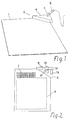
- the digitizing tablet shown in FIG. 1 is approximately 36 cm wide and 45 cm high. Its thickness is approximately 2 mm. It consists of a circuit board 1 provided with the usual conductor tracks and made of glass fiber reinforced plastic, which is sealed. Alternatively, one can be used as the carrier material for the conductor tracks flexixble plastic film can be used. The thickness of the finished tray can thus be reduced to less than 0.5 mm. A shield or housing is not required for measurement reasons.
- a housing 2 for the electronic control and measuring circuit is arranged on the upper right corner.
- the housing 2 has a triangular plan and consists of a lower part 3 and an upper part 4, which are firmly connected to one another and to the circuit board 1. Inside there is enough space for the necessary electronic components.
- a holder 5 for the pin 6 is provided on the upper part of the housing.
- This pen holder 5 can be connected to the housing 2 so that it is removable. It is preferably also rotatable relative to the housing, two positions being defined by a catch or the like. These two positions correspond to the ideal inclined position for right- and left-handed operation.
- a menu field 7 is shown in the top view of the tray shown in FIG. 2.
- the menu field can either be printed on the tray or it is only available via a template to be placed.
- Dashed line 8 shows the entire active area of the tablet.
- the menu is available on the measurement side and on the back. Both the measuring side and optionally the rear side can also be used as the measuring surface.
- the upper part is removed from the housing 2 for the electronic components in FIG.
- a particular advantage of the design of the digitizing tablet according to the invention is that the disruptive housing for the electronic components is located asymmetrically at one corner of the tablet and thus interferes with working on the tablet as little as possible.
- drawing devices such as rulers and the like, protruding beyond the tablet in both the vertical and horizontal directions can be applied.
- the asymmetrical arrangement naturally creates a region next to the electronics housing, which is shown in FIG. 2 for the menu field. The remaining work surface is again rectangular or square.
- a square or generally square outline shape is also possible for the electronics housing. This shape also has the main advantages of the asymmetrical arrangement.
Landscapes
- Engineering & Computer Science (AREA)
- General Engineering & Computer Science (AREA)
- Theoretical Computer Science (AREA)
- Human Computer Interaction (AREA)
- Physics & Mathematics (AREA)
- General Physics & Mathematics (AREA)
- Packaging Frangible Articles (AREA)
- Analysing Materials By The Use Of Radiation (AREA)
- Insertion, Bundling And Securing Of Wires For Electric Apparatuses (AREA)
- Medicinal Preparation (AREA)
- Medicines Containing Plant Substances (AREA)
- Length Measuring Devices With Unspecified Measuring Means (AREA)
- Other Investigation Or Analysis Of Materials By Electrical Means (AREA)
- Automatic Analysis And Handling Materials Therefor (AREA)
- Packages (AREA)
- Shielding Devices Or Components To Electric Or Magnetic Fields (AREA)
- Casings For Electric Apparatus (AREA)
Description
- Die Erfindung betrifft ein Digitalisiertablett mit einer im wesentlichen rechteckigen, Leiterbahnen enthaltenden Platine und elektronischen Ansteuerungs- und Meßschaltungen.
- Aus IEEE Communications Magazine, Bd. 24, Heft 7, Juli 1986, Seiten 18 bis 23, ist es bekannt, einen elektrolumineszierenden Anzeigebildschirm mit einer 0,4 mm dicken Polyesterfolie zu belegen, die InTiO₂-beschichtet ist, wodurch diese als Meßelement Verwendung finden kann. Das so entstandene, einige Zentimeter dicke Gerät hat dann zwei Funktionen: Anzeigebildschirm und durchsichtiges Tablett.
- Entsprechend der monitorartigen Bauweise müssen bei dieser Baueinheit handschriftliche Informationen an einer schräg stehenden Fläche eingegeben werden. Deshalb scheidet das maßgenaue Eingeben komplizierter Zeichnungen und dergleichen von Hand bei diesem System praktisch aus.
- Bekannte Digitalisiertabletts, die zum Eingeben von Zeichnungen und anderen komplizierteren Informationen von Hand, ggf. unter Zuhilfenahme von Zeichenwerkzeugen, bestimmt sind, haben meist eine Pult- bzw. Keilform oder eine flache Form mit einer Dicke von mindestens 5 bis 8 mm bis zu 150 mm. Dabei befindet sich die mit Leiterbahnen versehene Eingabeschicht in einem Rahmen. Die Pult- bzw. Keilform ergibt sich dabei dadurch, daß Platz für den Einbau der Elektronik geschaffen wird.
- Neuerdings gibt es auch Digitalisiertabletts, bei denen die elektronischen Ansteuerungs- und Meßschaltungen in einem separaten Gehäuse am Rande des Tabletts zusammengefaßt sind, so daß auf diese Weise das Tablett selbst nicht mehr pult- bzw. keilförmig ausgeführt ist.
- Dem Vorteil des wesentlich flacheren Tabletts steht der Nachteil entgegen, daß das Gehäuse für den Elektronikteil über die Oberfläche des Tabletts hinausragt und damit das freie Arbeiten auf dem Tablett behindert.
- Aus der DE 36 08 706 Cl ist ein Digitalisiertablett, bei dem ein Schaltungsgehäuse mit elektronischen Ansteuerungs- und Meßschaltungen an einem Rande des flachen Tabletts angeordnet ist, bekannt.
- Eine andere bekannte Lösung besteht darin, den Elektronikteil ganz vom Tablett zu trennen und in einem separaten Gehäuse unterzubringen, das so plaziert werden kann, daß es nicht stört, z.B. unter dem Tisch. Diese Lösung ist aber aus verschiedenen Gründen, z.B. wegen der erforderlichen langen Verbindungskabel, unhandlich.
- Der Erfindung liegt die Aufgabe zugrunde, ein Digitalisiertablett der eingangs genannten Art zu schaffen, das aufgrund sehr flacher Ausbildung vielseitig verwendbar und ergonomisch vorteilhaft ist und bei dem die Behinderung durch das Gehäuse für den Elektronikteil möglichst gering gehalten wird.
- Erfindungsgemäß wird diese Aufgabe mit den Merkmalen des kennzeichnenden Teils des Patentanspruchs 1 gelöst.
- Weiterbildungen der Erfindung ergeben sich aus den Unteransprüchen.
- Im folgenden ist anhand der beiliegenden Zeichnungen ein Ausführungsbeispiel der Erfindung näher beschrieben. Es zeigen
- Fig. 1
- eine perspektivische Darstellung eines Digitalisiertabletts nach der Erfindung, und
- Fig. 2
- eine Aufsicht auf eine Ausführungsform des erfindungsgemäßen Digitalisiertabletts.
- Das in Figur 1 gezeigte Digitalisiertablett ist ewa 36 cm breit und 45 cm hoch. Seine Dicke beträgt ca. 2 mm. Es besteht aus einer mit den üblichen Leiterbahnen versehenen Platine 1 aus glasfaserverstärktem Kunststoff, die versiegelt ist. Alternativ kann als Trägermaterial für die Leiterbahnen eine flexixble Kunststoffolie verwendet werden. Damit kann die Dicke des fertigen Tabletts bis auf weniger als 0,5 mm reduziert werden. Aus meßtechnischen Gründen wird eine Abschirmung oder ein Gehäuse nicht benötigt.
- An der rechten oberen Ecke ist ein Gehäuse 2 für die elektronische Ansteuerungs- und Meßschaltung angeordnet. Das Gehäuse 2 hat einen dreieckigen Grundriß und besteht aus einem unteren Teil 3 und einem Oberteil 4, die miteinander und mit der Platine 1 fest verbunden sind. Im Inneren ist genügend Platz für die erforderlichen elektronischen Bauelemente vorgesehen.
- Auf dem Oberteil des Gehäuses ist ein Halter 5 für den Stift 6 vorgesehen. Dieser Stifthalter 5 kann so mit dem Gehäuse 2 verbunden sein, daß er abnehmbar ist. Vorzugsweise ist er auch gegenüber dem Gehäuse drehbar, wobei zwei Positionen durch eine Raste oder dergleichen definiert werden. Diese zwei Positionen entsprechen der jeweils für rechts- und linkshändige Bedienung optimalen Schräglage.
- In der in Figur 2 gezeigten Aufsicht auf das Tablett ist ein Menüfeld 7 eingezeichnet. Das Menüfeld kann entweder auf dem Tablett aufgedruckt sein oder es ist nur über eine aufzulegende Schablone verfügbar. Die gestrichelte Linie 8 zeigt die gesamte aktive Fläche des Tabletts.
- Das Menuü ist auf der Meßseite und auf der Rückseite verfügbar. Auch kann sowohl die Meßseite als auch wahlweise die Rückseite als Meßfläche verwendet werden.
- Vom Gehäuse 2 für die elektronischen Bauelemente ist in Figur 2 der obere Teil abgenommen. Dadurch sind in schematischer Darstellung die einzelnen Bauelemente sichtbar. Sie umfassen zwei Stecker 9, 10, einen Mikroprozessor 11, einen Stecker 12 für ein sogenanntes PROM und eine Anschlußbuchse 13 für ein zu den Tablettleitern führendes Flachkabel (nicht gezeigt). Weitere Elemente, die in der Schaltung typischerweise vorhanden sind, wurden der Übersichtlichkeit halber in diesr schematischen Darstellung weggelassen. So sind beispielsweise die Verbindungsleiter der Elemente untereinander auf dieser Seite der im Gehäuse eingelegten Platine nicht sichtbar.
- Ein besonderer Vorteil der erfindungsgemäßen Ausbildung des Digitalisiertabletts besteht darin, daß sich das störende Gehäuse für die elektronischen Bauelemente asymmetrisch an einer Ecke des Tabletts befindet und damit das Arbeiten auf dem Tablett möglichst wenig beeinträchtigt. Insbesondere können sowohl in senkrechter als auch in waagerechter Richtung über das Tablett hinausragende Zeichengeräte, wie beispielsweise Lineale und dergleichen, angelegt werden. Außerdem ergibt sich durch die asymmetrische Anordnung sozusogen auf natürliche Weise ein Bereich neben dem Elektronikgehäuse, der in Figur 2 für das Menüfeld ausgewiesen ist. Die verbleibende Arbeitsfläche ist damit wiederum rechteckig oder quadratisch.
- Anstelle der dreieckigen Grundrißform ist auch eine quadratische oder allgemein viereckige Grundrißform für das Elektronikgehäuse möglich. Auch diese Form hat die wesentlichen Vorteile der asymmetrischen Anordnung.
Claims (4)
- Digitalisiertablett mit einer im wesentlichen rechteckigen, Leiterbahnen enthaltenden Platine und elektronischen Ansteuerungs- und Meßschaltungen,
dadurch gekennzeichnet, daß- die Dicke der Platine weniger als 3 mm beträgt,- die Schaltungen in einem an einer Ecke der Platine (1) integral angeordneten Schaltungsgehäuse (2) untergebracht sind, und- das Schaltungsgehäuse (2) eine im wesentlichen drei- oder viereckige Bodenfläche besitzt und mit zwei benachbarten Kanten derselben parallel zu Kanten des Digitalisiertabletts angeordnet ist. - Digitalisiertablett nach Anspruch 1,
dadurch gekennzeichnet, daß die Platine (1) aus einem mit den Leiterbahnen versehenen glasfaserverstärkten Kunststoff besteht. - Digitalisiertablett nach Anspruch 1,
dadurch gekennzeichnet, daß die Platine (1) aus einer mit den Leiterbahnen versehenen Kunststoffolie besteht. - Digitalisiertablett nach einem der vorhergehenden Ansprüche,
dadurch gekennzeichnet, daß ein Menüfeld (7) vorgesehen ist, das in einem Bereich zwischen dem Schaltungsgehäuse (2) und einer benachbarten weiteren Ecke der Platine angeordnet ist.
Applications Claiming Priority (2)
| Application Number | Priority Date | Filing Date | Title |
|---|---|---|---|
| CH668/89 | 1989-02-23 | ||
| CH668/89A CH679432A5 (de) | 1989-02-23 | 1989-02-23 |
Publications (2)
| Publication Number | Publication Date |
|---|---|
| EP0384269A1 EP0384269A1 (de) | 1990-08-29 |
| EP0384269B1 true EP0384269B1 (de) | 1995-05-10 |
Family
ID=4192357
Family Applications (2)
| Application Number | Title | Priority Date | Filing Date |
|---|---|---|---|
| EP90901790A Withdrawn EP0459990A1 (de) | 1989-02-23 | 1990-01-23 | Digitalisiertablett |
| EP90102787A Expired - Lifetime EP0384269B1 (de) | 1989-02-23 | 1990-02-13 | Digitalisiertablett |
Family Applications Before (1)
| Application Number | Title | Priority Date | Filing Date |
|---|---|---|---|
| EP90901790A Withdrawn EP0459990A1 (de) | 1989-02-23 | 1990-01-23 | Digitalisiertablett |
Country Status (7)
| Country | Link |
|---|---|
| EP (2) | EP0459990A1 (de) |
| AT (1) | ATE122484T1 (de) |
| AU (1) | AU4847090A (de) |
| CH (1) | CH679432A5 (de) |
| DE (2) | DE4004080A1 (de) |
| ES (1) | ES2072322T3 (de) |
| WO (1) | WO1990010266A1 (de) |
Families Citing this family (1)
| Publication number | Priority date | Publication date | Assignee | Title |
|---|---|---|---|---|
| GB2409725A (en) * | 2003-12-31 | 2005-07-06 | Erik Juel-Jacobsen | Input device for a computer or plotting device |
Citations (1)
| Publication number | Priority date | Publication date | Assignee | Title |
|---|---|---|---|---|
| DE3608706C1 (en) * | 1986-03-12 | 1987-11-05 | Aristo Graphic Systeme | Digitising tablet |
Family Cites Families (2)
| Publication number | Priority date | Publication date | Assignee | Title |
|---|---|---|---|---|
| DE8411193U1 (de) * | 1984-04-10 | 1984-09-13 | BWM Import u. Export GmbH Warenvertriebs KG, 8481 Thumsenreuth | Schreibunterlage |
| DE8514959U1 (de) * | 1985-05-21 | 1985-07-04 | Videograph Computer Gmbh, 6455 Erlensee | Digitizer Tablet |
-
1989
- 1989-02-23 CH CH668/89A patent/CH679432A5/de not_active IP Right Cessation
-
1990
- 1990-01-23 WO PCT/EP1990/000126 patent/WO1990010266A1/de not_active Ceased
- 1990-01-23 AU AU48470/90A patent/AU4847090A/en not_active Abandoned
- 1990-01-23 EP EP90901790A patent/EP0459990A1/de not_active Withdrawn
- 1990-02-10 DE DE4004080A patent/DE4004080A1/de not_active Ceased
- 1990-02-13 ES ES90102787T patent/ES2072322T3/es not_active Expired - Lifetime
- 1990-02-13 DE DE59009038T patent/DE59009038D1/de not_active Expired - Fee Related
- 1990-02-13 AT AT90102787T patent/ATE122484T1/de active
- 1990-02-13 EP EP90102787A patent/EP0384269B1/de not_active Expired - Lifetime
Patent Citations (1)
| Publication number | Priority date | Publication date | Assignee | Title |
|---|---|---|---|---|
| DE3608706C1 (en) * | 1986-03-12 | 1987-11-05 | Aristo Graphic Systeme | Digitising tablet |
Also Published As
| Publication number | Publication date |
|---|---|
| EP0384269A1 (de) | 1990-08-29 |
| DE4004080A1 (de) | 1990-08-30 |
| EP0459990A1 (de) | 1991-12-11 |
| DE59009038D1 (de) | 1995-06-14 |
| ES2072322T3 (es) | 1995-07-16 |
| WO1990010266A1 (de) | 1990-09-07 |
| AU4847090A (en) | 1990-09-26 |
| CH679432A5 (de) | 1992-02-14 |
| ATE122484T1 (de) | 1995-05-15 |
Similar Documents
| Publication | Publication Date | Title |
|---|---|---|
| DE69015792T2 (de) | Grundkarte mit Ausgleich. | |
| DE69507915T2 (de) | Kontaktlose Speicherkarte mit IC-Modul | |
| EP0013335A1 (de) | Anordnung zum elektrischen Verbinden einer Vielzahl von Anschlüssen | |
| DE2614741A1 (de) | Elektronischer taschenrechner | |
| EP0281746B1 (de) | Elektromechanische Braille-Zeile | |
| DE2245415B2 (de) | Kompakter elektronischer Rechner | |
| EP0729695A1 (de) | Anschlussfeld für steuergerät | |
| DE3017470A1 (de) | Mehrfachausdruck-dateneingabeeinrichtung | |
| DE2205084C3 (de) | Steckkarte mit elektronischem Schaltungsaufbau | |
| EP0594987B1 (de) | Elektrische Baugruppe | |
| EP0384269B1 (de) | Digitalisiertablett | |
| DE19509553C1 (de) | Abschirmhaube | |
| DE68920282T2 (de) | Schutz von elektronischen Schaltkreisen gegen statische Elektrizität. | |
| DE112021002286T5 (de) | Anzeigefeld und Verfahren zu dessen Herstellung | |
| EP0353706A2 (de) | Steuerpult für Werkzeugmaschinen | |
| EP0427012A1 (de) | Säulenführungsgestell | |
| EP0235733A1 (de) | Tastatur | |
| EP0093080B1 (de) | Tastatur | |
| DE4222940A1 (de) | Tastatur mit Maus-Eingabefeld | |
| DE2642157A1 (de) | Datenerfassungseinrichtung | |
| DE60034226T2 (de) | Datenlesegerät mit vertikaler Stauposition | |
| DE7826088U1 (de) | Schablonen zur ermittlung von aenderungsorten auf baugruppentraegern | |
| DE3116484A1 (de) | Vorrichtung mit textkarten fuer in baugruppentraeger einschiebbare baugruppen | |
| DE9112810U1 (de) | Personal-Computer | |
| DE2347441C3 (de) | Verfahren zur Befestigung von Anzeigeelementen an einer Grundplatte eines Rechners, die mit einem Gehäuseteil des Rechners verbunden wird |
Legal Events
| Date | Code | Title | Description |
|---|---|---|---|
| PUAI | Public reference made under article 153(3) epc to a published international application that has entered the european phase |
Free format text: ORIGINAL CODE: 0009012 |
|
| AK | Designated contracting states |
Kind code of ref document: A1 Designated state(s): AT BE CH DE ES FR GB IT LI LU NL SE |
|
| 17P | Request for examination filed |
Effective date: 19900914 |
|
| 17Q | First examination report despatched |
Effective date: 19920429 |
|
| GRAA | (expected) grant |
Free format text: ORIGINAL CODE: 0009210 |
|
| AK | Designated contracting states |
Kind code of ref document: B1 Designated state(s): AT BE CH DE ES FR GB IT LI LU NL SE |
|
| REF | Corresponds to: |
Ref document number: 122484 Country of ref document: AT Date of ref document: 19950515 Kind code of ref document: T |
|
| ET | Fr: translation filed | ||
| REF | Corresponds to: |
Ref document number: 59009038 Country of ref document: DE Date of ref document: 19950614 |
|
| REG | Reference to a national code |
Ref country code: ES Ref legal event code: FG2A Ref document number: 2072322 Country of ref document: ES Kind code of ref document: T3 |
|
| ITF | It: translation for a ep patent filed | ||
| GBT | Gb: translation of ep patent filed (gb section 77(6)(a)/1977) |
Effective date: 19950620 |
|
| RAP2 | Party data changed (patent owner data changed or rights of a patent transferred) |
Owner name: KONTRON ELEKTRONIK GMBH |
|
| RAP2 | Party data changed (patent owner data changed or rights of a patent transferred) |
Owner name: MUELLER, UDO Owner name: KONTRON ELEKTRONIK GMBH |
|
| NLT2 | Nl: modifications (of names), taken from the european patent patent bulletin |
Owner name: KONTRON ELEKTRONIK GMBH |
|
| PG25 | Lapsed in a contracting state [announced via postgrant information from national office to epo] |
Ref country code: LU Free format text: LAPSE BECAUSE OF NON-PAYMENT OF DUE FEES Effective date: 19960229 |
|
| PLBE | No opposition filed within time limit |
Free format text: ORIGINAL CODE: 0009261 |
|
| STAA | Information on the status of an ep patent application or granted ep patent |
Free format text: STATUS: NO OPPOSITION FILED WITHIN TIME LIMIT |
|
| 26N | No opposition filed | ||
| PGFP | Annual fee paid to national office [announced via postgrant information from national office to epo] |
Ref country code: SE Payment date: 19970203 Year of fee payment: 8 |
|
| PGFP | Annual fee paid to national office [announced via postgrant information from national office to epo] |
Ref country code: ES Payment date: 19970206 Year of fee payment: 8 |
|
| PGFP | Annual fee paid to national office [announced via postgrant information from national office to epo] |
Ref country code: GB Payment date: 19970210 Year of fee payment: 8 |
|
| PGFP | Annual fee paid to national office [announced via postgrant information from national office to epo] |
Ref country code: CH Payment date: 19970212 Year of fee payment: 8 Ref country code: BE Payment date: 19970212 Year of fee payment: 8 |
|
| PGFP | Annual fee paid to national office [announced via postgrant information from national office to epo] |
Ref country code: AT Payment date: 19970225 Year of fee payment: 8 |
|
| PGFP | Annual fee paid to national office [announced via postgrant information from national office to epo] |
Ref country code: NL Payment date: 19970228 Year of fee payment: 8 Ref country code: FR Payment date: 19970228 Year of fee payment: 8 |
|
| PG25 | Lapsed in a contracting state [announced via postgrant information from national office to epo] |
Ref country code: GB Free format text: LAPSE BECAUSE OF NON-PAYMENT OF DUE FEES Effective date: 19980213 Ref country code: AT Free format text: LAPSE BECAUSE OF NON-PAYMENT OF DUE FEES Effective date: 19980213 |
|
| PG25 | Lapsed in a contracting state [announced via postgrant information from national office to epo] |
Ref country code: SE Free format text: LAPSE BECAUSE OF NON-PAYMENT OF DUE FEES Effective date: 19980214 Ref country code: ES Free format text: LAPSE BECAUSE OF NON-PAYMENT OF DUE FEES Effective date: 19980214 |
|
| PGFP | Annual fee paid to national office [announced via postgrant information from national office to epo] |
Ref country code: DE Payment date: 19980218 Year of fee payment: 9 |
|
| PG25 | Lapsed in a contracting state [announced via postgrant information from national office to epo] |
Ref country code: LI Free format text: LAPSE BECAUSE OF NON-PAYMENT OF DUE FEES Effective date: 19980228 Ref country code: FR Free format text: THE PATENT HAS BEEN ANNULLED BY A DECISION OF A NATIONAL AUTHORITY Effective date: 19980228 Ref country code: CH Free format text: LAPSE BECAUSE OF NON-PAYMENT OF DUE FEES Effective date: 19980228 Ref country code: BE Free format text: LAPSE BECAUSE OF NON-PAYMENT OF DUE FEES Effective date: 19980228 |
|
| BERE | Be: lapsed |
Owner name: KONTRON ELEKTRONIK G.M.B.H. Effective date: 19980228 |
|
| PG25 | Lapsed in a contracting state [announced via postgrant information from national office to epo] |
Ref country code: NL Free format text: LAPSE BECAUSE OF NON-PAYMENT OF DUE FEES Effective date: 19980901 |
|
| GBPC | Gb: european patent ceased through non-payment of renewal fee |
Effective date: 19980213 |
|
| REG | Reference to a national code |
Ref country code: CH Ref legal event code: PL |
|
| EUG | Se: european patent has lapsed |
Ref document number: 90102787.0 |
|
| NLV4 | Nl: lapsed or anulled due to non-payment of the annual fee |
Effective date: 19980901 |
|
| REG | Reference to a national code |
Ref country code: FR Ref legal event code: ST |
|
| PG25 | Lapsed in a contracting state [announced via postgrant information from national office to epo] |
Ref country code: DE Free format text: LAPSE BECAUSE OF NON-PAYMENT OF DUE FEES Effective date: 19991201 |
|
| REG | Reference to a national code |
Ref country code: ES Ref legal event code: FD2A Effective date: 20000503 |
|
| PG25 | Lapsed in a contracting state [announced via postgrant information from national office to epo] |
Ref country code: IT Free format text: LAPSE BECAUSE OF NON-PAYMENT OF DUE FEES;WARNING: LAPSES OF ITALIAN PATENTS WITH EFFECTIVE DATE BEFORE 2007 MAY HAVE OCCURRED AT ANY TIME BEFORE 2007. THE CORRECT EFFECTIVE DATE MAY BE DIFFERENT FROM THE ONE RECORDED. Effective date: 20050213 |