EP0379330A2 - Circuit intégré avec assemblage de porte - Google Patents
Circuit intégré avec assemblage de porte Download PDFInfo
- Publication number
- EP0379330A2 EP0379330A2 EP90300429A EP90300429A EP0379330A2 EP 0379330 A2 EP0379330 A2 EP 0379330A2 EP 90300429 A EP90300429 A EP 90300429A EP 90300429 A EP90300429 A EP 90300429A EP 0379330 A2 EP0379330 A2 EP 0379330A2
- Authority
- EP
- European Patent Office
- Prior art keywords
- gate array
- grid
- integrated circuit
- pattern
- metal
- Prior art date
- Legal status (The legal status is an assumption and is not a legal conclusion. Google has not performed a legal analysis and makes no representation as to the accuracy of the status listed.)
- Granted
Links
Images
Classifications
-
- H—ELECTRICITY
- H01—ELECTRIC ELEMENTS
- H01L—SEMICONDUCTOR DEVICES NOT COVERED BY CLASS H10
- H01L27/00—Devices consisting of a plurality of semiconductor or other solid-state components formed in or on a common substrate
- H01L27/02—Devices consisting of a plurality of semiconductor or other solid-state components formed in or on a common substrate including semiconductor components specially adapted for rectifying, oscillating, amplifying or switching and having at least one potential-jump barrier or surface barrier; including integrated passive circuit elements with at least one potential-jump barrier or surface barrier
- H01L27/04—Devices consisting of a plurality of semiconductor or other solid-state components formed in or on a common substrate including semiconductor components specially adapted for rectifying, oscillating, amplifying or switching and having at least one potential-jump barrier or surface barrier; including integrated passive circuit elements with at least one potential-jump barrier or surface barrier the substrate being a semiconductor body
- H01L27/10—Devices consisting of a plurality of semiconductor or other solid-state components formed in or on a common substrate including semiconductor components specially adapted for rectifying, oscillating, amplifying or switching and having at least one potential-jump barrier or surface barrier; including integrated passive circuit elements with at least one potential-jump barrier or surface barrier the substrate being a semiconductor body including a plurality of individual components in a repetitive configuration
- H01L27/118—Masterslice integrated circuits
- H01L27/11803—Masterslice integrated circuits using field effect technology
- H01L27/11807—CMOS gate arrays
Definitions
- This invention relates to an integrated circuit gate array configured from a chain of polysilicon gate field effect transistors.
- Gate arrays are used extensively to fabricate integrated circuits which perform customer specialized functions, and as such are a subclass of products known as application specific integrated circuits (ASICs).
- ASICs application specific integrated circuits
- the semiconductor devices of the gate arrays are designed into base patterns and fabricated into wafers for customer specific functional interconnection during metallization. Consequently, the integrated circuit semiconductor devices can be interconnected to perform the logic functions desired by a customer in the relatively short time needed to form the metallization patterns.
- the metallization by which the pre-existing transistors and other active devices in the base set are interconnected to form functional configurations now preferably utilizes two or more metallization layers, a pattern of contacts to connect from the metallization layers to the semiconductor regions, and selectively defined vias to interconnect the successive metallization patterns.
- CMOS complementary MOS
- Designing a gate array base set or pattern which maximizes the number of electronic functions performed on a semiconductor chip of defined areas is not merely a matter of shrinking field effect transistor dimensions.
- Integrated circuit design rules impose a number of constraints on the interconnection of the transistors.
- the gate array design must satisfy minimum polysilicon width dimensions, minimum spacing between polysilicon conductors, minimum metal width dimensions, minimum spacing between metal conductors, minimum dimensions for contacts, minimum dimensions for vias, and constraints as to vertical placement of the various consecutive layers.
- the gate array technical community has yet to reach a consensus as to the optimum and preferred approach for maximizing functional density per unit area of semiconductor chip, with one end of the present spectrum preferring the "sea-of-gates" approach, in which the whole surface is covered with field effect transistors capable of being interconnected, and the other end of the present spectrum represented by gate arrays which use elongated patterns of field effect transistors separated by wide wiring channel regions nominally twice the area of the transistor regions.
- gate isolation A relatively recent refinement in the design of gate arrays has been the introduction of gate isolation.
- a chain of field effect transistors often individually referred to as gates or cells, is defined in the substrate with the source region of one serving as the drain region of the other in a continuum separated only by successive gate electrodes with underlying channel regions.
- Electrical isolation of active transistors is accomplished by tying the gate electrodes of the peripheral transistors to the power supply or the ground potential, respectively for the p-channel and n-channel devices. The interconnection as well as the tying is performed during metallization. Connection of the gates to perform isolation and electronic functions is preferably undertaken with computer aided design equipment in response to functional descriptions entered by a circuit designer.
- an integrated circuit gate array configured from a chain of polysilicon gate field effect transistors, characterized by a first metal layer pattern referenced to a grid pattern and adapted for computer aided design; a second metal layer pattern referenced to the grid; a source/drain contact pattern contacting source/drain regions of the field effect transistors and referenced to the grid; an intermetal via pattern referenced to the grid; and a gate polysilicon pattern referenced to the half grid.
- each transistor cell is capable of having a metal layer extend across the transistor, in parallel to the gate electrode, with full capability to make contact to both the substrate and polysilicon layers, and to have vias between the successive metal layers, without violating classic design rules.
- an integrated circuit gate array configured in polysilicon gate field effect transistors in chains of adjacent and complementary pairs, characterized by the presence of channel regions between adjacent chain pairs having a channel width suitable to form three metal lines.
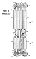
- FIG. 1 illustrates an arrangement of relatively recent vintage as set forth in U.S Patent No. 4,745,084.
- Fig. 1 generally shows a succession of p-channel transistors 1 and closely located n-channel transistors 2 situated in respective chains with successive p-channel source/drain diffusion regions 3 and n-channel source/drain diffusion regions 4, separated by a respective successions of gate electrodes 6 and 7, and associated channel regions beneath each such gate electrode.
- a versatile interconnect architecture maximizes the utilization of gates per unit chip area, and as such is very important if chip size and associated cost are to be competitive.
- gate array designs have tended to migrate into somewhat opposite camps.
- the first camp employs the concept known as "sea-of-gates", which is characterized in that the whole of the semiconductor surface is covered by field effect transistor gates/cells. Interconnection is undertaken with the recognition that the placement of interconnect metal patterns over many cells will effectively preclude their use as active devices in functional groupings.
- User experience has shown that the routability of a sea-of-gates array is in the range of 40%, for exemplary two-input NAND gate groupings. In terms of functional capability, this would mean that a chip having 100,000 gates is capable of utilizing approximately 40,000 gates in standardized functional groupings.
- the class of gate array designs which incorporates wide channels between chains of active gates/cells, channels nominally equivalent to the pitch of 20 metal lines. For such arrangements, it is not unusual to experience 90% routing efficiency.
- the wide channel gate array configuration can only have approximately 33,000 gates (1/3 of 100,000 gates), which if routed at 90% efficiency provides an effective yield of 30,000 gates for functional groups.
- the present invention exceeds both configurations as to the routable and usable gates for a semiconductor chip of comparable size.
- the structural constraints and dimensional design rules imposed upon the embodiment in Fig. 2 are representative of an advanced gate array technology.
- vias interconnecting two metal layers may not overlap an edge of an underlying polysilicon layer.
- vias, contacts, and all metal patterns must be referenced to a grid suitable for computer manipulation.
- minimum relative spacing the minimum polysilicon spacing is one grid. The same minimum of one grid applies to the first metal layer spacing, while the second metal layer spacing is expanded to 1.5 grids.
- the contacts and vias are required to be one grid in width, and must be bounded by source/drain, polysilicon, metal 1 or metal 2 region extending at least one-half grid beyond the contact or via pattern.
- the widths of the polysilicon, first metal, and second metal lines are also constrained respectively to one grid, 1.5 grids, and two grids in minimum dimension.
- an identified objective was to create a cell structure which matches the cell pitch to the lowest density metal pitch, in this case the second metal pitch, without unduly constraining the pattern of the first metal, the location of the contacts, or the location of the vias.
- the goal must, however, be accomplished in the context of a computer aided design grid pattern which facilitates automated layout and routing.
- the desired objective was accomplished as embodied in Fig. 2 by displacing the polysilicon level gate electrode to a half grid alignment, while referencing the first metal layer patterns, the second metal layer patterns, the contacts, and the vias to the unit grid pattern.
- the solution is particularly appropriate when the grid pattern essentially coincides with the minimum dimensions of the polysilicon layer in width and relative spacing.
- This alignment of the polysilicon layer to the half grid in a gate array architecture is particularly suited to a gate isolated cell gate array base design, in that the computer aided design tools can operate unencumbered on the basis of a highly structured and readily defined grid pattern.
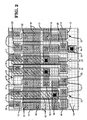
- Fig. 2 illustrates a portion of the embodying gate isolated gate array pattern in the context of a grid pattern 13 as might appear on a video display of a computer aided design system.
- the first metal layer is shown by a shaded pattern 14.
- the second metal layer 16 is shown by cross-hatching.
- the polysilicon layer patterns for the transistor gate electrodes are shown by heavy outlines at 17.
- the source/drain diffusions in the semiconductor substrate are shown as dotted regions 18 between successive gate electrodes 17.
- Contacts which make connection between the first metal layer and the semiconductor substrate in the source/drain regions are shown at 19, while contacts between the first metal layer and the transistor well regions are shown at 21.
- Contacts between the first metal layer and the polysilicon are done in the polysilicon pad regions, generally 22, and are identified by reference numeral 23.
- the vias connecting first metal to second metal are shown at 24. Note that the edge of the polysilicon pattern is always situated with reference to the half grid, while the first metal pattern is defined with reference to the grid pattern itself.
- the two grid minimum width of first metal pattern at each contact coincides and matches the half grid placement of the polysilicon layer in the pad regions 22. Further note that the contacts 19 from the first metal to the substrate are fully situated within the two grid dimension.
- the recognized prevailing objective is to define a cell structure in which the pitch of the cells is equal to the minimum design rule pitch of the metal layers, while retaining full capability to make contact connections from the metal to the polysilicon gate or the source/drain, and to make via connections between the metal layers within each cell.
- This capability as to interconnection is illustrated in the succession of cells at 26 and 27, where there appear within the pitch spacing of one cell contacts between first metal and the polysilicon pad, contacts between first metal and the substrate, and vias between first and second metal, without violations of minimum dimensions, relative spacings or vias locations, and within the framework of a grid suitable to operate on a computer aided design system.
- the polysilicon gate electrode pattern could be aligned to the grid pattern without violating the one grid minimum relative spacing dimension and still retain the contact access from the first metal to the polysilicon or semiconductor substrate, the translated polysilicon gate pattern would violate via location design constraints in the creation of an overlap with the polysilicon pattern.
- Analogous translations of the first or second metal patterns relative to such grid aligned polysilicon pattern will show similar fundamental constraint violations in the placement of contacts or vias, or in the alternative, restrictions on the use of vias within the source/drain regions of the cells. Increasing the metal pitch is obviously not a meaningful solution if functional density is an important consideration.
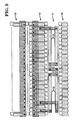
- FIG. 3 An expanded depiction of the embodied cell architecture appears in Fig. 3 for purposes of illustrating another refinement.
- the preferred arrangement in Fig. 3 includes parallel and adjacent chains of p-channel transistors 28 and n-channel transistors 29 separated by a wiring channel 31.
- the wiring channel is defined to have a width equal to the pitch dimension of three cells, and as such is capable of conveying three adjacent metal or diffused conductive lines.
- a channel width corresponding to the pitch of three metal lines provides an optimum balance between the area allocated to wiring and the area allocated to cells on the basis of usable gates. For example, increasing the width of channel 31 permits greater interconnect utilization of the cells, but results in a reallocation of chip area. The consequential cell gate count loss exceeds the functional gain attributed to greater interconnection. Similarly, decreasing the channel width results in an unused gate increase greater than the gain in cell count.
- Fig. 3 also illustrates another feature of the present invention.
- Diffused resistors 32 are formed in channel region 31 for immediate and direct interconnection to the cells of the gate array. Unconnected resistors 32 do not restrict the use of the channel 31 for wiring in that they are situated within the substrate and electrically isolated from both the metal 1 and metal 2 wiring levels. As a consequence, a multiplicity of the resistors can be formed during the creation of the base set for the gate array. The resistors are then available for discretionary interconnection without otherwise affecting the cell count of the array. As a further feature, the physical proximity of such diffused resistors optimizes the likelihood of matching both electrical and temperature parameters. For example, the set of resistors 32 shown in channel 31 are interconnected in a cross-coupled manner to maximize matching as may be required for a precise differential application.
- the half grid alignment of the gate polysilicon layer, in combination with a channel region of width equal to the pitch of three cells provides a gate array with exceptionally high usable gate density.
- This architecture provides a cell pitch which matches the metallization pitch while providing full ability to form contacts to the substrate or polysilicon layers, and vias within each source/drain region of the cell transistors.
- the three metallization line channel width provides the optimum balance between cell count and cell utilization for typical random logic applications.
- the width of channel 31 is obviously related to the number of metallization layers used to fabricate the gate array product.
- a high density gate array architecture using a channel based CMOS gate isolated configuration which has the transistor gate electrode pitch and metallization pitch relatively coincide while permitting full contact formation to both substrate and gate polysilicon, and which further includes an optimized channel width to maximize the functions implemented per unit area of a semiconductor chip.
- the preferred embodiment features a gate array structure and architecture which is refined to maximize metal interconnect level routability and usable cells density for a channel type gate isolated CMOS product, and involves a single polysilicon layer gate electrode base cell structure with multiple metal layers for interconnect.
Applications Claiming Priority (2)
| Application Number | Priority Date | Filing Date | Title |
|---|---|---|---|
| US07/297,355 US4928160A (en) | 1989-01-17 | 1989-01-17 | Gate isolated base cell structure with off-grid gate polysilicon pattern |
| US297355 | 1994-08-29 |
Publications (3)
| Publication Number | Publication Date |
|---|---|
| EP0379330A2 true EP0379330A2 (fr) | 1990-07-25 |
| EP0379330A3 EP0379330A3 (fr) | 1992-02-19 |
| EP0379330B1 EP0379330B1 (fr) | 1997-10-22 |
Family
ID=23145973
Family Applications (1)
| Application Number | Title | Priority Date | Filing Date |
|---|---|---|---|
| EP90300429A Expired - Lifetime EP0379330B1 (fr) | 1989-01-17 | 1990-01-16 | Circuit intégré avec assemblage de porte |
Country Status (4)
| Country | Link |
|---|---|
| US (1) | US4928160A (fr) |
| EP (1) | EP0379330B1 (fr) |
| JP (1) | JP3154411B2 (fr) |
| DE (1) | DE69031603T2 (fr) |
Families Citing this family (33)
| Publication number | Priority date | Publication date | Assignee | Title |
|---|---|---|---|---|
| US5410173A (en) * | 1991-01-28 | 1995-04-25 | Kikushima; Ken'ichi | Semiconductor integrated circuit device |
| US5764533A (en) * | 1995-08-01 | 1998-06-09 | Sun Microsystems, Inc. | Apparatus and methods for generating cell layouts |
| US5990502A (en) * | 1995-12-29 | 1999-11-23 | Lsi Logic Corporation | High density gate array cell architecture with metallization routing tracks having a variable pitch |
| US5923060A (en) * | 1996-09-27 | 1999-07-13 | In-Chip Systems, Inc. | Reduced area gate array cell design based on shifted placement of alternate rows of cells |
| US5977574A (en) * | 1997-03-28 | 1999-11-02 | Lsi Logic Corporation | High density gate array cell architecture with sharing of well taps between cells |
| US5981987A (en) | 1997-12-02 | 1999-11-09 | Nurlogic Design, Inc. | Power ground metallization routing in a semiconductor device |
| JP3526450B2 (ja) * | 2001-10-29 | 2004-05-17 | 株式会社東芝 | 半導体集積回路およびスタンダードセル配置設計方法 |
| US7492013B2 (en) * | 2005-06-27 | 2009-02-17 | International Business Machines Corporation | Systems and arrangements to interconnect components of a semiconductor device |
| US7956421B2 (en) | 2008-03-13 | 2011-06-07 | Tela Innovations, Inc. | Cross-coupled transistor layouts in restricted gate level layout architecture |
| US9563733B2 (en) | 2009-05-06 | 2017-02-07 | Tela Innovations, Inc. | Cell circuit and layout with linear finfet structures |
| US9009641B2 (en) | 2006-03-09 | 2015-04-14 | Tela Innovations, Inc. | Circuits with linear finfet structures |
| US9035359B2 (en) | 2006-03-09 | 2015-05-19 | Tela Innovations, Inc. | Semiconductor chip including region including linear-shaped conductive structures forming gate electrodes and having electrical connection areas arranged relative to inner region between transistors of different types and associated methods |
| US8541879B2 (en) | 2007-12-13 | 2013-09-24 | Tela Innovations, Inc. | Super-self-aligned contacts and method for making the same |
| US8448102B2 (en) | 2006-03-09 | 2013-05-21 | Tela Innovations, Inc. | Optimizing layout of irregular structures in regular layout context |
| US7763534B2 (en) | 2007-10-26 | 2010-07-27 | Tela Innovations, Inc. | Methods, structures and designs for self-aligning local interconnects used in integrated circuits |
| US8658542B2 (en) | 2006-03-09 | 2014-02-25 | Tela Innovations, Inc. | Coarse grid design methods and structures |
| US8653857B2 (en) | 2006-03-09 | 2014-02-18 | Tela Innovations, Inc. | Circuitry and layouts for XOR and XNOR logic |
| US8839175B2 (en) | 2006-03-09 | 2014-09-16 | Tela Innovations, Inc. | Scalable meta-data objects |
| US7446352B2 (en) | 2006-03-09 | 2008-11-04 | Tela Innovations, Inc. | Dynamic array architecture |
| US9230910B2 (en) | 2006-03-09 | 2016-01-05 | Tela Innovations, Inc. | Oversized contacts and vias in layout defined by linearly constrained topology |
| US7888705B2 (en) | 2007-08-02 | 2011-02-15 | Tela Innovations, Inc. | Methods for defining dynamic array section with manufacturing assurance halo and apparatus implementing the same |
| US8667443B2 (en) | 2007-03-05 | 2014-03-04 | Tela Innovations, Inc. | Integrated circuit cell library for multiple patterning |
| US8713493B2 (en) * | 2007-12-21 | 2014-04-29 | Cadence Design Systems, Inc. | System and method for solving connection violations |
| CN101946186B (zh) * | 2007-12-21 | 2014-04-23 | 益华公司 | 用于解决连接冲突的系统和方法 |
| US8453094B2 (en) | 2008-01-31 | 2013-05-28 | Tela Innovations, Inc. | Enforcement of semiconductor structure regularity for localized transistors and interconnect |
| US7939443B2 (en) | 2008-03-27 | 2011-05-10 | Tela Innovations, Inc. | Methods for multi-wire routing and apparatus implementing same |
| MY152456A (en) | 2008-07-16 | 2014-09-30 | Tela Innovations Inc | Methods for cell phasing and placement in dynamic array architecture and implementation of the same |
| US9122832B2 (en) | 2008-08-01 | 2015-09-01 | Tela Innovations, Inc. | Methods for controlling microloading variation in semiconductor wafer layout and fabrication |
| US8661392B2 (en) | 2009-10-13 | 2014-02-25 | Tela Innovations, Inc. | Methods for cell boundary encroachment and layouts implementing the Same |
| US9159627B2 (en) | 2010-11-12 | 2015-10-13 | Tela Innovations, Inc. | Methods for linewidth modification and apparatus implementing the same |
| US10127340B2 (en) | 2016-09-30 | 2018-11-13 | Taiwan Semiconductor Manufacturing Company, Ltd. | Standard cell layout, semiconductor device having engineering change order (ECO) cells and method |
| CN110767661B (zh) * | 2018-07-27 | 2023-07-07 | 京东方科技集团股份有限公司 | 阵列基板及其制备方法、显示装置 |
| CN109492273B (zh) * | 2018-10-22 | 2022-11-15 | 珠海一微半导体股份有限公司 | 一种基于通孔的自动打孔方法 |
Citations (10)
| Publication number | Priority date | Publication date | Assignee | Title |
|---|---|---|---|---|
| JPS6074647A (ja) * | 1983-09-30 | 1985-04-26 | Fujitsu Ltd | 半導体集積回路装置 |
| JPS6074646A (ja) * | 1983-09-30 | 1985-04-26 | Fujitsu Ltd | 半導体集積回路装置 |
| JPS6074648A (ja) * | 1983-09-30 | 1985-04-26 | Fujitsu Ltd | 半導体集積回路装置 |
| US4549131A (en) * | 1981-12-26 | 1985-10-22 | Olympus Optical Company Limited | Semiconductor device and technique which employs normally unused interconnection elements as resistor circuit elements |
| US4570176A (en) * | 1984-04-16 | 1986-02-11 | At&T Bell Laboratories | CMOS Cell array with transistor isolation |
| US4591993A (en) * | 1983-11-21 | 1986-05-27 | International Business Machines Corporation | Methodology for making logic circuits |
| US4613940A (en) * | 1982-11-09 | 1986-09-23 | International Microelectronic Products | Method and structure for use in designing and building electronic systems in integrated circuits |
| US4627152A (en) * | 1985-05-24 | 1986-12-09 | International Business Machines Corporation | Automatic layout for cascode voltage switch logic |
| US4661815A (en) * | 1984-10-03 | 1987-04-28 | Fujitsu Limited | Gate array integrated device having mixed single column type and matrix type arrays |
| DE3714598A1 (de) * | 1986-05-23 | 1987-11-26 | Mitsubishi Electric Corp | Integrierte halbleiterschaltung |
Family Cites Families (6)
| Publication number | Priority date | Publication date | Assignee | Title |
|---|---|---|---|---|
| US4161662A (en) * | 1976-01-22 | 1979-07-17 | Motorola, Inc. | Standardized digital logic chip |
| JPS5890758A (ja) * | 1981-11-25 | 1983-05-30 | Mitsubishi Electric Corp | 相補形集積回路装置 |
| JPS58122771A (ja) * | 1982-01-14 | 1983-07-21 | Nec Corp | 半導体集積回路装置 |
| JPS6065547A (ja) * | 1983-09-20 | 1985-04-15 | Sharp Corp | 半導体装置 |
| US4633571A (en) * | 1984-04-16 | 1987-01-06 | At&T Bell Laboratories | Method of manufacturing a CMOS cell array with transistor isolation |
| US4745084A (en) * | 1986-11-12 | 1988-05-17 | Vlsi Technology, Inc. | Method of making a customized semiconductor integrated device |
-
1989
- 1989-01-17 US US07/297,355 patent/US4928160A/en not_active Expired - Lifetime
-
1990
- 1990-01-12 JP JP00368490A patent/JP3154411B2/ja not_active Expired - Lifetime
- 1990-01-16 DE DE69031603T patent/DE69031603T2/de not_active Expired - Lifetime
- 1990-01-16 EP EP90300429A patent/EP0379330B1/fr not_active Expired - Lifetime
Patent Citations (10)
| Publication number | Priority date | Publication date | Assignee | Title |
|---|---|---|---|---|
| US4549131A (en) * | 1981-12-26 | 1985-10-22 | Olympus Optical Company Limited | Semiconductor device and technique which employs normally unused interconnection elements as resistor circuit elements |
| US4613940A (en) * | 1982-11-09 | 1986-09-23 | International Microelectronic Products | Method and structure for use in designing and building electronic systems in integrated circuits |
| JPS6074647A (ja) * | 1983-09-30 | 1985-04-26 | Fujitsu Ltd | 半導体集積回路装置 |
| JPS6074646A (ja) * | 1983-09-30 | 1985-04-26 | Fujitsu Ltd | 半導体集積回路装置 |
| JPS6074648A (ja) * | 1983-09-30 | 1985-04-26 | Fujitsu Ltd | 半導体集積回路装置 |
| US4591993A (en) * | 1983-11-21 | 1986-05-27 | International Business Machines Corporation | Methodology for making logic circuits |
| US4570176A (en) * | 1984-04-16 | 1986-02-11 | At&T Bell Laboratories | CMOS Cell array with transistor isolation |
| US4661815A (en) * | 1984-10-03 | 1987-04-28 | Fujitsu Limited | Gate array integrated device having mixed single column type and matrix type arrays |
| US4627152A (en) * | 1985-05-24 | 1986-12-09 | International Business Machines Corporation | Automatic layout for cascode voltage switch logic |
| DE3714598A1 (de) * | 1986-05-23 | 1987-11-26 | Mitsubishi Electric Corp | Integrierte halbleiterschaltung |
Non-Patent Citations (4)
| Title |
|---|
| IEEE JOURNAL OF SOLID-STATE CIRCUITS, vol. SC-20, no. 2, April 1985, New York NOIJE et al. "Advanced CMOS Gate Array Architecture Combinining "Gate Isolation"- and Programmable Reuting Channels" page 469-480 * |
| PATENT ABSTRACTS OF JAPAN, E field, vol. 9, no. 212, August 29, 1985 THE PATENT OFFICE JAPANESE GOVERNEMENT pages 83, 84 E 339; & JP-A-60 074 647 (FUJITSU) * |
| PATENT ABSTRACTS OF JAPAN, unexamined applications, E field, vol. 9, no. 212, August 29, 1985 THE PATENT OFFICE JAPANESE GOVERNEMENT pages 83,84 E 339; & JP-A-60 074 646 (FUJITSU) * |
| PATENT ABSTRACTS OF JAPAN, unexamined applications, E field, vol. 9, no. 212, August 29, 1985 THE PATENT OFFICE JAPANESE GOVERNEMENT pages 83,84 E 339; & JP-A-60 074 648 (FUJITSU) * |
Also Published As
| Publication number | Publication date |
|---|---|
| EP0379330B1 (fr) | 1997-10-22 |
| US4928160A (en) | 1990-05-22 |
| JPH02234469A (ja) | 1990-09-17 |
| EP0379330A3 (fr) | 1992-02-19 |
| DE69031603T2 (de) | 1998-05-20 |
| JP3154411B2 (ja) | 2001-04-09 |
| DE69031603D1 (de) | 1997-11-27 |
Similar Documents
| Publication | Publication Date | Title |
|---|---|---|
| US4928160A (en) | Gate isolated base cell structure with off-grid gate polysilicon pattern | |
| KR100375753B1 (ko) | 반도체 소자의 파워/그라운드 금속 경로 설정 | |
| US5684311A (en) | Base cell for BiCMOS and CMOS gate arrays | |
| US4412237A (en) | Semiconductor device | |
| KR100433025B1 (ko) | 반도체장치,반도체집적회로장치,플립플롭회로,배타적논리합회로,멀티플렉서및가산기 | |
| EP0203025B1 (fr) | Matrice de portes à isolation réduite | |
| US4161662A (en) | Standardized digital logic chip | |
| US6987293B2 (en) | Semiconductor integrated circuit device and standard cell placement design method | |
| US4851892A (en) | Standard cell array having fake gate for isolating devices from supply voltages | |
| US4668972A (en) | Masterslice semiconductor device | |
| US20080180132A1 (en) | Semiconductor device and method of fabricating the same | |
| JPS647508B2 (fr) | ||
| US5869900A (en) | Sea-of-cells array of transistors | |
| US4525809A (en) | Integrated circuit | |
| KR100306335B1 (ko) | 반도체집적회로장치 | |
| US5229629A (en) | Semiconductor integrated circuit having improved cell layout | |
| US5416431A (en) | Integrated circuit clock driver having improved layout | |
| US5063430A (en) | Semiconductor integrated circuit device having standard cells including internal wiring region | |
| US5434436A (en) | Master-slice type semiconductor integrated circuit device having multi-power supply voltage | |
| EP0092176B1 (fr) | Cellule de base pour réseau de portes à circuit intégré | |
| EP0119059A2 (fr) | Circuit intégré semi-conducteur comportant une structure de matrice de portes | |
| USH512H (en) | Automated universal array | |
| EP0113828B1 (fr) | Plaquette semi-conductrice du type à tranche maîtresse comportant une cellule FET multi-fonctionnelle | |
| KR100216882B1 (ko) | 반도체 집적회로장치 | |
| GB2121601A (en) | Uncommitted logic integrated circuit array |
Legal Events
| Date | Code | Title | Description |
|---|---|---|---|
| PUAI | Public reference made under article 153(3) epc to a published international application that has entered the european phase |
Free format text: ORIGINAL CODE: 0009012 |
|
| AK | Designated contracting states |
Kind code of ref document: A2 Designated state(s): DE GB NL |
|
| PUAL | Search report despatched |
Free format text: ORIGINAL CODE: 0009013 |
|
| AK | Designated contracting states |
Kind code of ref document: A3 Designated state(s): DE GB NL |
|
| 17P | Request for examination filed |
Effective date: 19920729 |
|
| 17Q | First examination report despatched |
Effective date: 19940412 |
|
| RAP1 | Party data changed (applicant data changed or rights of an application transferred) |
Owner name: NCR INTERNATIONAL INC. |
|
| RAP1 | Party data changed (applicant data changed or rights of an application transferred) |
Owner name: AT&T GLOBAL INFORMATION SOLUTIONS INTERNATIONAL IN |
|
| RAP1 | Party data changed (applicant data changed or rights of an application transferred) |
Owner name: AT&T GLOBAL INFORMATION SOLUTIONS INTERNATIONAL IN Owner name: HYUNDAI ELECTRONICS AMERICA |
|
| RAP1 | Party data changed (applicant data changed or rights of an application transferred) |
Owner name: SYMBIOS LOGIC INC. Owner name: HYUNDAI ELECTRONICS AMERICA Owner name: AT&T GLOBAL INFORMATION SOLUTIONS INTERNATIONAL IN |
|
| GRAG | Despatch of communication of intention to grant |
Free format text: ORIGINAL CODE: EPIDOS AGRA |
|
| RAP1 | Party data changed (applicant data changed or rights of an application transferred) |
Owner name: NCR INTERNATIONAL, INC. Owner name: HYUNDAI ELECTRONICS AMERICA Owner name: SYMBIOS LOGIC INC. |
|
| GRAH | Despatch of communication of intention to grant a patent |
Free format text: ORIGINAL CODE: EPIDOS IGRA |
|
| GRAH | Despatch of communication of intention to grant a patent |
Free format text: ORIGINAL CODE: EPIDOS IGRA |
|
| GRAA | (expected) grant |
Free format text: ORIGINAL CODE: 0009210 |
|
| AK | Designated contracting states |
Kind code of ref document: B1 Designated state(s): DE GB NL |
|
| REF | Corresponds to: |
Ref document number: 69031603 Country of ref document: DE Date of ref document: 19971127 |
|
| NLT1 | Nl: modifications of names registered in virtue of documents presented to the patent office pursuant to art. 16 a, paragraph 1 |
Owner name: NCR INTERNATIONAL, INC;HYUNDAI ELECTRONICS AMERICA |
|
| PLBE | No opposition filed within time limit |
Free format text: ORIGINAL CODE: 0009261 |
|
| STAA | Information on the status of an ep patent application or granted ep patent |
Free format text: STATUS: NO OPPOSITION FILED WITHIN TIME LIMIT |
|
| 26N | No opposition filed | ||
| REG | Reference to a national code |
Ref country code: GB Ref legal event code: IF02 |
|
| NLS | Nl: assignments of ep-patents |
Owner name: HYUNDAI ELECTRONICS AMERICA Owner name: NCR INTERNATIONAL, INC Owner name: HYNIX SEMICONDUCTOR INC. |
|
| NLT1 | Nl: modifications of names registered in virtue of documents presented to the patent office pursuant to art. 16 a, paragraph 1 |
Owner name: HYNIX SEMICONDUCTOR AMERICA INC. Owner name: NCR INTERNATIONAL, INC |
|
| REG | Reference to a national code |
Ref country code: GB Ref legal event code: 732E |
|
| NLS | Nl: assignments of ep-patents |
Owner name: NCR INTERNATIONAL, INC Effective date: 20060913 Owner name: MAGNACHIP SEMICONDUCTOR LTD. Effective date: 20060913 |
|
| REG | Reference to a national code |
Ref country code: GB Ref legal event code: 732E |
|
| REG | Reference to a national code |
Ref country code: GB Ref legal event code: 732E |
|
| PGFP | Annual fee paid to national office [announced via postgrant information from national office to epo] |
Ref country code: NL Payment date: 20090124 Year of fee payment: 20 Ref country code: DE Payment date: 20090302 Year of fee payment: 20 |
|
| PGFP | Annual fee paid to national office [announced via postgrant information from national office to epo] |
Ref country code: GB Payment date: 20090129 Year of fee payment: 20 |
|
| REG | Reference to a national code |
Ref country code: GB Ref legal event code: PE20 Expiry date: 20100115 |
|
| NLV7 | Nl: ceased due to reaching the maximum lifetime of a patent |
Effective date: 20100116 |
|
| PG25 | Lapsed in a contracting state [announced via postgrant information from national office to epo] |
Ref country code: GB Free format text: LAPSE BECAUSE OF EXPIRATION OF PROTECTION Effective date: 20100115 |
|
| PG25 | Lapsed in a contracting state [announced via postgrant information from national office to epo] |
Ref country code: NL Free format text: LAPSE BECAUSE OF EXPIRATION OF PROTECTION Effective date: 20100116 |
|
| PG25 | Lapsed in a contracting state [announced via postgrant information from national office to epo] |
Ref country code: DE Free format text: LAPSE BECAUSE OF EXPIRATION OF PROTECTION Effective date: 20100116 |