EP0377454B1 - Bildlesegerät - Google Patents
Bildlesegerät Download PDFInfo
- Publication number
- EP0377454B1 EP0377454B1 EP90100101A EP90100101A EP0377454B1 EP 0377454 B1 EP0377454 B1 EP 0377454B1 EP 90100101 A EP90100101 A EP 90100101A EP 90100101 A EP90100101 A EP 90100101A EP 0377454 B1 EP0377454 B1 EP 0377454B1
- Authority
- EP
- European Patent Office
- Prior art keywords
- image
- diffraction element
- light
- reading apparatus
- image reading
- Prior art date
- Legal status (The legal status is an assumption and is not a legal conclusion. Google has not performed a legal analysis and makes no representation as to the accuracy of the status listed.)
- Expired - Lifetime
Links
Images


Classifications
-
- G—PHYSICS
- G02—OPTICS
- G02B—OPTICAL ELEMENTS, SYSTEMS OR APPARATUS
- G02B5/00—Optical elements other than lenses
- G02B5/18—Diffraction gratings
- G02B5/1876—Diffractive Fresnel lenses; Zone plates; Kinoforms
- G02B5/188—Plurality of such optical elements formed in or on a supporting substrate
- G02B5/1885—Arranged as a periodic array
-
- G—PHYSICS
- G02—OPTICS
- G02B—OPTICAL ELEMENTS, SYSTEMS OR APPARATUS
- G02B27/00—Optical systems or apparatus not provided for by any of the groups G02B1/00 - G02B26/00, G02B30/00
- G02B27/42—Diffraction optics, i.e. systems including a diffractive element being designed for providing a diffractive effect
- G02B27/4205—Diffraction optics, i.e. systems including a diffractive element being designed for providing a diffractive effect having a diffractive optical element [DOE] contributing to image formation, e.g. whereby modulation transfer function MTF or optical aberrations are relevant
- G02B27/4211—Diffraction optics, i.e. systems including a diffractive element being designed for providing a diffractive effect having a diffractive optical element [DOE] contributing to image formation, e.g. whereby modulation transfer function MTF or optical aberrations are relevant correcting chromatic aberrations
-
- G—PHYSICS
- G02—OPTICS
- G02B—OPTICAL ELEMENTS, SYSTEMS OR APPARATUS
- G02B27/00—Optical systems or apparatus not provided for by any of the groups G02B1/00 - G02B26/00, G02B30/00
- G02B27/42—Diffraction optics, i.e. systems including a diffractive element being designed for providing a diffractive effect
- G02B27/4205—Diffraction optics, i.e. systems including a diffractive element being designed for providing a diffractive effect having a diffractive optical element [DOE] contributing to image formation, e.g. whereby modulation transfer function MTF or optical aberrations are relevant
- G02B27/4227—Diffraction optics, i.e. systems including a diffractive element being designed for providing a diffractive effect having a diffractive optical element [DOE] contributing to image formation, e.g. whereby modulation transfer function MTF or optical aberrations are relevant in image scanning systems
-
- G—PHYSICS
- G02—OPTICS
- G02B—OPTICAL ELEMENTS, SYSTEMS OR APPARATUS
- G02B27/00—Optical systems or apparatus not provided for by any of the groups G02B1/00 - G02B26/00, G02B30/00
- G02B27/42—Diffraction optics, i.e. systems including a diffractive element being designed for providing a diffractive effect
- G02B27/4272—Diffraction optics, i.e. systems including a diffractive element being designed for providing a diffractive effect having plural diffractive elements positioned sequentially along the optical path
-
- G—PHYSICS
- G02—OPTICS
- G02B—OPTICAL ELEMENTS, SYSTEMS OR APPARATUS
- G02B3/00—Simple or compound lenses
- G02B3/0006—Arrays
- G02B3/0037—Arrays characterized by the distribution or form of lenses
- G02B3/0056—Arrays characterized by the distribution or form of lenses arranged along two different directions in a plane, e.g. honeycomb arrangement of lenses
-
- H—ELECTRICITY
- H04—ELECTRIC COMMUNICATION TECHNIQUE
- H04N—PICTORIAL COMMUNICATION, e.g. TELEVISION
- H04N1/00—Scanning, transmission or reproduction of documents or the like, e.g. facsimile transmission; Details thereof
- H04N1/024—Details of scanning heads ; Means for illuminating the original
- H04N1/028—Details of scanning heads ; Means for illuminating the original for picture information pick-up
- H04N1/03—Details of scanning heads ; Means for illuminating the original for picture information pick-up with photodetectors arranged in a substantially linear array
- H04N1/031—Details of scanning heads ; Means for illuminating the original for picture information pick-up with photodetectors arranged in a substantially linear array the photodetectors having a one-to-one and optically positive correspondence with the scanned picture elements, e.g. linear contact sensors
- H04N1/0311—Details of scanning heads ; Means for illuminating the original for picture information pick-up with photodetectors arranged in a substantially linear array the photodetectors having a one-to-one and optically positive correspondence with the scanned picture elements, e.g. linear contact sensors using an array of elements to project the scanned image elements onto the photodetectors
- H04N1/0312—Details of scanning heads ; Means for illuminating the original for picture information pick-up with photodetectors arranged in a substantially linear array the photodetectors having a one-to-one and optically positive correspondence with the scanned picture elements, e.g. linear contact sensors using an array of elements to project the scanned image elements onto the photodetectors using an array of optical fibres or rod-lenses
-
- G—PHYSICS
- G02—OPTICS
- G02B—OPTICAL ELEMENTS, SYSTEMS OR APPARATUS
- G02B3/00—Simple or compound lenses
- G02B3/02—Simple or compound lenses with non-spherical faces
- G02B3/08—Simple or compound lenses with non-spherical faces with discontinuous faces, e.g. Fresnel lens
-
- Y—GENERAL TAGGING OF NEW TECHNOLOGICAL DEVELOPMENTS; GENERAL TAGGING OF CROSS-SECTIONAL TECHNOLOGIES SPANNING OVER SEVERAL SECTIONS OF THE IPC; TECHNICAL SUBJECTS COVERED BY FORMER USPC CROSS-REFERENCE ART COLLECTIONS [XRACs] AND DIGESTS
- Y02—TECHNOLOGIES OR APPLICATIONS FOR MITIGATION OR ADAPTATION AGAINST CLIMATE CHANGE
- Y02E—REDUCTION OF GREENHOUSE GAS [GHG] EMISSIONS, RELATED TO ENERGY GENERATION, TRANSMISSION OR DISTRIBUTION
- Y02E10/00—Energy generation through renewable energy sources
- Y02E10/50—Photovoltaic [PV] energy
- Y02E10/52—PV systems with concentrators
Definitions
- the present invention relates generally to image reading apparatuses and, more particularly to reducing the size of and simplifying the structure of a lens array in an image reading apparatus for illuminating an image with light from an illuminating light source, imaging light from the image onto a line sensor through the lens array and electrically reading image information.
- Office machines or communication apparatuses such as copiers or facsimiles comprise image reading apparatuses which optically read image information represented on the original of paper or drawings and convert the read information into an electric signal to be taken out.
- the image reading apparatus with a representative structure comprises a light source, an optical lens and an image sensor.
- the apparatus illuminates the original having image information with white light from the light source, projects reflected light thereof being optically reduced in size onto a line sensor such as a CCD (Charge Coupled Device) image sensor through the optical lens, converts this projected light into an electrical signal and reads image information.
- CCD Charge Coupled Device
- a spacing between the original and a light acceptance plane of image information is increased, resulting in an increase in the size of the apparatus.
- a reflecting mirror for bending an optical path of rays of light from an image is usually employed in the optical system to reduce the size of the apparatus.
- the provision of a device such as the reflecting mirror results in a complicated structure of the apparatus with a disadvantage that the apparatus is not effectively made compact.
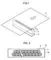
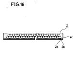
- this image reading apparatus comprises a light emitting diode 1 (not shown) to serve as a light source, a refractive index profile type lens array 2 constituting the optical system, and a line sensor 3 including a plurality of CCD image sensors for converting image information into an electric signal.
- the refractive index profile type lens array 2 comprises a large number of focusing lens elements 2a of a cylindrical shape with a diameter of approximately 1 mm. These focusing lens elements 2a are interposed between frame plates 2b on both sides thereof.
- the frame plate 2b is formed of a glass fabric based epoxy resin black lamination plate (FRP) having almost the same thermal expansion property as the focusing lens element 2a so as to reduce thermal distortion and increase strength thereof.
- Black silicon rubber resin 2c is filled in spaces between the focusing lens elements 2a and the frame plate 2b. This silicon rubber resin 2c serves to remove flare light around the focusing lens elements 2a.
- Illumination light is first directed from the light emitting diode 1 to the surface of the original 4.
- Light from the image, reflecting on the surface of the original 4 is introduced into the refractive index profile type lens array 2 to be focused. This light is then transmitted through the refractive index profile type lens array 2 and is then imaged on the surface of the line sensor 3.
- the line sensor 3 converts this light from the image into an electrical signal to read image information.
- the image reading apparatus employing the refractive index profile type lens array 2 can be reduced in size, it provides a disadvantage that a manufacturing cost of the apparatus is increased due to a difficulty in manufacturing the refractive index profile type lens array 2.
- the refractive index profile type lens array 2 also has another disadvantage that the removal of the flare light by the black silicon rubber resin 2c as a filler decreases the efficiency in utilizing incident light.
- a lens array which can be more easily manufactured than the lens arrays of the above described apparatuses is known from Patent Abstracts of Japan, Vol. 12, No. 259 (P-733) [3106], 21 July 1988 & JP-A-63-46403.
- This lens array comprises a plurality of micro-Fresnel lenses on both the front and rear faces of a rectangular base plate.
- Patent Abstracts of Japan, Vol. 7, No. 280 (E-216) [1425], 14 December 1983 & JP-A-58-159059 disclose a lens system in which a sensor is formed on the lower face of a lens substrate.
- Patent Abstracts of Japan, Vol. 7, No. 258 (E-211) [1403], 17 November 1983 & JP-A-58-143665 disclose an image sensor arrangement in which a plurality of light emitting elements and photoelectric converting devices are arranged within a housing.
- the image reading apparatus of the present invention is defined by the teaching of appended claim 1. According to this teaching, the length of the lens arrangement or optical focusing means is reduced in that the light within the base of said means is reflected at least twice between the entrance position and the exit position. Thereby, the width of the base is somewhat broadened against the width of a base in which the light is irradiated directly from the entrance position to the exit position, however, the length is reduced considerably. Therefore, over all the size of an image reading apparatus can be reduced against the size of a prior art apparatus.
- the distances between the object and the optical focusing means and/or the distance between said means and the sensor are adjustable in a wider range. Further, it is possible to prevent chromatic aberration by using such plural diffraction elements.
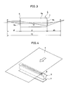
- the image reading apparatus comprises a light emitting diode 1 (not shown) and a line sensor 3 including a diffraction element array 5 and a CCD image sensor.
- the line sensor 3 is provided at a position opposing to the original 4 through the diffraction element array 5.
- the diffraction element array 5 comprises a rectangular base 5a formed of a transparent material such as glass or plastic.
- One plane of the base 5a in an elongated direction comprises a plane 6 of incidence, while the other plane opposite this incident plane 6 comprises a plane 7 of emission.
- a plurality of diffraction elements 8 such as Fresnel lens are arranged planar on the surfaces of the incident plane 6 and the emission plane 7.
- the diffraction elements 8 cover the overall surfaces of the incident plane 6 and the plane 7 of emission.
- Image information P on the surface of the original 4 which accepts illuminating light from the light emitting diode is directed toward the incident plane 6 of the diffraction element array 5, transmissively through a diffraction element 8a provided on this incident plane 6 and enters the diffraction element array 5.
- the image information P is transmitted through a diffraction element 8b formed on the plane 7 of the diffraction element array 5 to form an erecting real image at the position of Q.
- the image information P is then photoelectrically converted by the line sensor 3 (not shown) placed in the position of Q to be read.
- a distance between the image information P on the surface of the original 4 and the erecting real image formed on the line sensor 3, i.e., the conjugate length TC is represented by a total sum of a differential distance l1 on the side of an object, a differential distance l2 on the side of an image and a thickness Z of the base of the diffraction element array 5.
- the differential distances l1 and l2 on the respective sides of the object and the image are determined by the form of the grating of the diffraction elements 8a and 8b provided respectively on the incident plane 6 and the emission plane 7 of the diffraction element array 5.
- Each diffraction element such as Fresnel lens has the form of uniform micro-spaced and curved grating.
- a method of manufacturing such an diffraction element comprises the steps of producing a mold with the form of grating formed by an electron beam direct writing method, reduction type exposure and the like, and then producing a replica by employing this mold. This method enables mass production of this diffraction element and thus a considerable reduction in cost compared to the conventional refractive index profile type lens array or the like.
- a diffraction efficiency of the diffraction element can be twice or more that of a step type diffraction element by employing a blazed diffraction grating, and it becomes possible to inhibit cross-talk due to a diffraction of an unrequired diffraction degree, resulting in no particular problems in practical use.
- the diffraction elements 8 are formed without any spacing over the entire surface of the incident plane 6 or the emission plane 7 of the base 5a. This formation enables utilization efficiency of light to be enhanced compared to the conventional refractive index profile type lens array 2.
- the image reading apparatus of the first embodiment in accordance with the present invention will now be described with reference to Figs. 4 and 5.
- This embodiment is featured by employing a prism 9 for the base 5a of the diffraction element array 5 compared to the first embodiment.
- the overall structure of the apparatus is identical to that of the prestage, as shown in Fig. 4.
- the prism 9 of this embodiment is a polygonal prism comprising a plane 6 of incidence, a plane 7 of emission, and four planes of reflection, 10a, 10b, 10c and 10d.
- Diffraction elements 8a and 8b are provided respectively on the incident plane 6 and the emission plane 7 of this prism 9.
- an optical path of light from an image which is transmitted through the diffraction element 8a formed on the incident plane 6 and then enters the prism 9, is first bent at the reflection plane 10a of the prism 9 and then at the reflection plane 10b to once form an inverted real image Q1. Further, this optical path is then bent at the reflection planes 10c and 10d and is transmitted through the diffraction element 8b formed on the emission plane 7. The light transmitted is then introduced outside to form an erecting image at a predetermined position of Q. In the diffraction element array 5 employing this prism 9, a shorter straight distance of the optical path is achieved on due to the bending of the optical path of the light within the prism 9.
- a thickness Z of the prism 9 can be reduced compared to that of the diffraction element array 5 shown in Fig. 3. This results in a reduction in the conjugate length TC of the diffraction element array and thus a reduction in the size of the apparatus.
- the second embodiment which is a variation of the first embodiment, is shown in Fig. 6.
- other diffraction elements 8c-8f are further provided respectively on the reflection planes 10a-10d of the prism 9 shown in Fig. 5 so as to decrease an accuracy required for the angle of reflection in the prism. That is, in the reflection caused by utilizing the reflection planes of the prism 9 shown in Fig. 5, a position of the imaging point Q is deviated due to an angular error of the reflection planes.
- a direction of the diffraction of the luminous flux is determined by spacings in a grating, so that this direction is least affected by an angular error of a plane on which the diffraction element is formed.
- gratings on the diffraction elements 8c-8f provided on the reflection planes of this prism 9 so that these diffraction elements 8c-8f may serve as lenses in the same manner as the diffraction elements 8a and 8b provided respectively on the incident plane 6 and the emission plane 7.
- Such a construction results in enhanced mass-productivity in the form of the diffraction elements 8a-8f provided on the incident plane 6, the emission plane 7 and the reflection planes of the prism 9, respectively.
- This further causes the differential distances l1 and l2 on the respective sides of the object and the image to be adjustable in a wider range, so that the differential distances can arbitrarily be determined in accordance with the structure of the system of the image reading apparatus.
- the transmissive structure of the plurality of diffraction elements 8a-8f shown in Fig. 6 prevents an occurrence of chromatic aberration. That is, the diffraction elements, in general, can eliminate in principle the chromatic aberration for light with a single wavelength.
- a general image reading apparatus employs a light emitting diode which emits light with multiwavelength to an illuminating light source for the original. Therefore, the chromatic aberration occurs with only a diffraction element on one plane.
- grating patterns are formed on the diffraction elements so as to mutually correct the chromatic aberration by diffraction at the plurality of diffraction elements on two or more planes, so that a clearly visible image without any chromatic aberration can be read.
- This action will be described in more detail in case of employing two diffraction elements, for example.
- grating patterns of the first and second diffraction elements can be designed by numerical calculation of a computer so that the second diffraction element corrects this change in the angle of diffraction at the first diffraction element to direct the light toward the same focal point.
- This effect of correction of the chromatic aberration is not limitative to this combination of two diffraction elements, but can be attained with a combination of a plurality of diffraction elements.
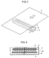
- Fig. 7 is a perspective view of a schematic structure of the image reading apparatus of this embodiment.
- the basic structure of the apparatus of this embodiment is the same as those shown in Figs. 1 and 4.
- the feature of this embodiment resides in the form of arrangement of the diffraction elements 8 in the diffraction element array 5 shown in Fig. 8.
- the diffraction element array 5 comprises a rectangular base 5a.
- One plane of the base 5a in an elongated direction comprises a plane 6 of incidence of light from an image, while the other plane opposing to this incident plane 6 comprises a plane 7 of emission (not shown).
- a diffraction element array 11 for incidence and a diffraction element array 12 for reflection are formed on the incident plane 6 of the base 5a.
- a diffraction element array 12 for reflection is formed on the emission plane 7 of the base 5a.
- the diffraction element array 12 for reflection is formed on the emission plane 7 of the base 5a.
- Image information P on the surface of the original 4 is illuminated with illumination light from the light emitting diode 1, and light from the image is then focused by and transmissively through a diffraction element 8a constituting the diffraction element array 11 for incidence, formed on the incident plane 6 of the array 5, thereby being introduced into the element 8a.
- the light introduced in the diffraction element 8a is diffracted by a diffraction element 8c formed on the emission plane 7 of the base 5a and then reaches a diffraction element 8d formed on the incident plane 6 of the base 5a.
- This light is then diffracted by this diffraction element 8d and reaches a diffraction element 8b formed on the emission plane 7 of the base 5a.
- the image information P is emitted outside by the diffraction element 8b to form an erecting real image at a predetermined position Q.
- an optical path of the light from the image is bent within the diffraction element array 5 by forming the diffraction elements 8c, 8d for reflection respectively on the incident plane 6 and the emission plane 7 of the array 5, thereby reducing a straight distance of the optical path.
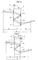
- the fourth embodiment of the image reading apparatus according to the present invention will now be described with reference to Figs. 10 and 11.
- This embodiment is characterized in that the light emitting diode 1 serving as a light source is integrally formed with the diffraction element array 5. That is, the light emitting diode 1 is adhesively fixed onto the emission plane 7 of the diffraction element array 5, as shown in Figs. 10 and 11.
- the light emitting diode 1 to be attached comprises a semiconductor chip la of the light emitting diode and a package portion lb thereof.
- Diffraction elements 8e and 8f for focusing light emitted from the light emitting diode 1 are provided respectively on the emission plane 7 of the diffraction element array 5, positioned in an emission direction of the light emitting diode 1, and on the incident plane 6 of the array 5.
- This provision of the diffraction elements 8e and 8f requires no converging lens to be provided at an emitting position of the package of the light emitting diode 1 and thus results in a simplified structure of the light emitting diode 1.
- the size of the apparatus is reduced by integrally forming the light emitting diode 1 with the diffraction element array 5.
- the fifth embodiment of the present invention is a variation of the fourth embodiment described above.
- the diffraction element 8f provided on the surface of the incident plane 6 of the diffraction element array 5 and the diffraction element 8a provided at an incident position of light from an image are integrally formed together to be employed as a converging lens of the light emitting diode 1.
- illumination light directed from the light emitting diode 1 is focused by the diffraction element 8e and therewith diffracted toward the diffraction element 8a provided on the incident plane 6.
- a luminous flux from the light emitting diode 1 is in the same optical path direction as minus first order diffraction light of the diffraction element 8a, it is diffracted toward an image P and is appropriately converged to illuminate the image.
- the light reflected from the image P due to this illumination light is again transmitted through the diffraction element 8a to be introduced into the diffraction element array 5.
- the diffraction element 8a serves both as a lens for focusing and transmitting the light from the image and as the converging lens for the light emitting diode.
- the image reading apparatus which is a variation of the fifth embodiment described above, is characterized by a simplified structure of the light emitting diode 1. That is, as shown in Fig. 13, the semiconductor chip la of the light emitting diode 1 is directly and adhesively fixed onto the surface of the diffraction element array 5 at a predetermined position of the emission plane 7 of the array 5. This structure requires no package of the light emitting diode 1 and thus attains the simpler and smaller-size apparatus.
- the image reading apparatus is characterized by integrally forming the line sensor 3 to be attached onto the emission plane 7 of the diffraction element array 5 compared to the sixth embodiment described above. That is, as shown in Fig. 14,the line sensor 3 is fixedly attached to a position on the emission plane 7, from which light from an image is emitted outside. The diffraction element 8b which has been provided at this position is omitted. Increasing effects, as lenses, of the respective diffraction elements 8a-8c and 8d, provided on the diffraction element array 5 results in such a structure that the light from the image is imaged on the surface of the line sensor 3 attached onto the emission plane 7 of the diffraction element array 5.
- This structure requires no differential distance l2 on the side of the object, which is required in the above described embodiment, and thus the conjugate length TC of the diffraction element array 5 is substantially reduced to achieve the reduction in the size of the apparatus.
- the diffraction grating such as Fresnel lens or hologram is employed for the diffraction element in the above embodiment.
- a lens array of the image reading apparatus is configured by forming the diffraction elements on the incident plane and the emission plane of the base, an image reading apparatus with low cost and available for mass production by employing replica manufacturing technology or the like can be implemented.
- this embodiment is structured such that the light from the image is bent within the lens array so as to be able to reduce the length of the optical path thereof, the reductions in the thickness of the lens array and in the optical path of the optical system can achieve the reduction in the size of the apparatus.
- the integral formation of the lens array with the light source or the image sensor in the image reading apparatus results in the apparatus with the simplified structure and the reduced size.
Landscapes
- Physics & Mathematics (AREA)
- General Physics & Mathematics (AREA)
- Optics & Photonics (AREA)
- Engineering & Computer Science (AREA)
- Multimedia (AREA)
- Signal Processing (AREA)
- Facsimile Heads (AREA)
- Diffracting Gratings Or Hologram Optical Elements (AREA)
- Photovoltaic Devices (AREA)
Claims (8)
- Bildlesegerät mit:a) einer Lichtquelle (1), die die Oberfläche eines Gegenstands mit Beleuchtungslicht beleuchtet;b) einer optischen Fokussiereinrichtung (5) zum Empfangen von vom Gegenstand reflektiertem Licht innerhalb einer Eintrittsposition, um das Licht zu einer Austrittsposition zu übertragen, und zum Ausbilden eines Bilds des Gegenstands an einer vorgegebenen Bildposition, wobei die optische Fokussiereinrichtung folgendes aufweist:b1) einen transparenten Träger (5a) mit einer Eintrittsebene, die die Eintrittsposition enthält, und einer Emissionsebene, die die Austrittsposition enthält;b2) ein erstes Beugungselement (8a), das an der Eintrittsposition ausgebildet ist; undb3) ein zweites Beugungselement; undc) einer Bildsensoranordnung (3), die an der Bildposition vorhanden ist und das Bild in ein elektrisches Signal umsetzt, um das Bild des Gegenstands zu lesen;
dadurch gekennzeichnet, daß die optische Fokussiereinrichtung (5) so ausgebildet ist, daß sie das Licht mindestens zweimal innerhalb des Trägers (5a) zwischen der Eintrittsposition und der Austrittsposition reflektiert. - Bildlesegerät nach Anspruch 1, bei dem der Träger (5) ein V-förmiges Prisma mit einem eintrittsseitigen Schenkel und einem austrittsseitigen Schenkel ist, von denen jeder eine Innenfläche, die zur Innenseite des "V" gerichtet ist, und eine Außenseite, die zur Außenseite des "V" gerichtet ist, aufweist, wodurch das Licht von der Eintrittsposition zunächst von einer ersten Reflexionsposition an der Innenseite des Eintrittsschenkels zu einer zweiten Reflexionsposition an der Außenseite des Schenkels reflektiert wird, von dort zu einer dritten Reflexionsposition an der Außenseite des Austrittsschenkels von dort zu einer vierten Reflexionsposition an der Innenseite des Austrittsschenkels und schließlich von dort zur Austrittsposition, an der das zweite Beugungselement (8b) vorhanden ist.
- Bildlesegerät nach Anspruch 2, bei dem ein Beugungselement (8c, 8d, 8e, 8f) an jeder der ersten bis zweiten Reflexionsposition vorhanden ist.
- Bildlesegerät nach Anspruch 1, bei dem der Träger (5) ein rechteckiger Träger mit einer Eintrittsfläche mit der Eintrittsposition und einer Austrittsfläche mit der Austrittsposition ist, in welchem Träger das Licht dann, wenn es an der Eintrittsposition eintritt, durch das erste Beugungselement (8a) zu einer Position im zweiten Beugungselement (8c) reflektiert wird, das auf der Austrittsfläche liegt, dort zu einer Position reflektiert wird, an der ein drittes Beugungselement (8d) liegt, und dann zur Austrittsposition reflektiert wird.
- Bildlesegerät nach Anspruch 4, bei dem ein viertes Beugungselement (8b) an der Austrittsposition angeordnet ist.
- Bildlesegerät nach Anspruch 4, bei dem die Bildposition mit der Austrittsposition übereinstimmt und daher der Bildsensor direkt auf dem Träger (5) an der Austrittsposition angeordnet ist.
- Bildlesegerät nach einem der vorstehenden Ansprüche, bei dem die Beugungselemente (8a, 8b, 8c, 8d, 8e, 8f) so angeordnet sind, daß sie für eine Kompensation betreffend chromatische Aberration sorgen.
- Bildlesegerät nach einem der vorstehenden Ansprüche, dadurch gekennzeichnet, daß die Beugungselemente (8a, 8b, 8c, 8d, 8e, 8f) Fresnel-Linsen sind.
Applications Claiming Priority (2)
| Application Number | Priority Date | Filing Date | Title |
|---|---|---|---|
| JP1001678A JP2568434B2 (ja) | 1989-01-06 | 1989-01-06 | 画像読取装置 |
| JP1678/89 | 1989-01-06 |
Publications (3)
| Publication Number | Publication Date |
|---|---|
| EP0377454A2 EP0377454A2 (de) | 1990-07-11 |
| EP0377454A3 EP0377454A3 (de) | 1992-01-02 |
| EP0377454B1 true EP0377454B1 (de) | 1994-11-02 |
Family
ID=11508170
Family Applications (1)
| Application Number | Title | Priority Date | Filing Date |
|---|---|---|---|
| EP90100101A Expired - Lifetime EP0377454B1 (de) | 1989-01-06 | 1990-01-03 | Bildlesegerät |
Country Status (4)
| Country | Link |
|---|---|
| US (1) | US4998806A (de) |
| EP (1) | EP0377454B1 (de) |
| JP (1) | JP2568434B2 (de) |
| DE (1) | DE69013694T2 (de) |
Families Citing this family (13)
| Publication number | Priority date | Publication date | Assignee | Title |
|---|---|---|---|---|
| JPH03226067A (ja) * | 1990-01-30 | 1991-10-07 | Canon Inc | カラー画像読取り装置 |
| JPH04233863A (ja) * | 1990-12-28 | 1992-08-21 | Rohm Co Ltd | イメージセンサ |
| JPH0563909A (ja) * | 1991-08-28 | 1993-03-12 | Canon Inc | カラー画像読取装置 |
| US5340978A (en) * | 1992-09-30 | 1994-08-23 | Lsi Logic Corporation | Image-sensing display panels with LCD display panel and photosensitive element array |
| US5529936A (en) * | 1992-09-30 | 1996-06-25 | Lsi Logic Corporation | Method of etching a lens for a semiconductor solid state image sensor |
| US5760834A (en) * | 1992-09-30 | 1998-06-02 | Lsi Logic | Electronic camera with binary lens element array |
| US5495411A (en) * | 1993-12-22 | 1996-02-27 | Ananda; Mohan | Secure software rental system using continuous asynchronous password verification |
| JPH08331320A (ja) * | 1995-05-31 | 1996-12-13 | Fujitsu Ltd | 画像読み取り装置 |
| US5636057A (en) * | 1995-02-10 | 1997-06-03 | Ecolux Inc. | Prismatic toroidal lens and traffic signal light using this lens |
| US5734155A (en) * | 1995-06-07 | 1998-03-31 | Lsi Logic Corporation | Photo-sensitive semiconductor integrated circuit substrate and systems containing the same |
| US5770889A (en) * | 1995-12-29 | 1998-06-23 | Lsi Logic Corporation | Systems having advanced pre-formed planar structures |
| JPH10229473A (ja) | 1997-01-21 | 1998-08-25 | Xerox Corp | 二重焦点深度入力スキャナ |
| US6570505B1 (en) | 1997-12-30 | 2003-05-27 | Gelcore Llc | LED lamp with a fault-indicating impedance-changing circuit |
Family Cites Families (8)
| Publication number | Priority date | Publication date | Assignee | Title |
|---|---|---|---|---|
| JPS5592072A (en) * | 1978-12-29 | 1980-07-12 | Nippon Telegr & Teleph Corp <Ntt> | Photoelectric conversion unit |
| JPS57210772A (en) * | 1981-06-19 | 1982-12-24 | Canon Inc | Reading device |
| JPS58143665A (ja) * | 1982-02-19 | 1983-08-26 | Fuji Xerox Co Ltd | 密着型読取装置 |
| JPS58159059A (ja) * | 1982-03-17 | 1983-09-21 | Ricoh Co Ltd | イメ−ジセンサ− |
| JPS5921172A (ja) * | 1982-04-23 | 1984-02-03 | Fuji Xerox Co Ltd | 撮像装置 |
| JPS62145960A (ja) * | 1985-12-20 | 1987-06-30 | Fuji Xerox Co Ltd | 画像読取装置 |
| JPS6346403A (ja) * | 1986-08-14 | 1988-02-27 | Omron Tateisi Electronics Co | イメ−ジ・デイバイス |
| JPS63208355A (ja) * | 1987-02-24 | 1988-08-29 | Matsushita Graphic Commun Syst Inc | 原稿読取装置 |
-
1989
- 1989-01-06 JP JP1001678A patent/JP2568434B2/ja not_active Expired - Fee Related
- 1989-12-28 US US07/458,442 patent/US4998806A/en not_active Expired - Fee Related
-
1990
- 1990-01-03 DE DE69013694T patent/DE69013694T2/de not_active Expired - Fee Related
- 1990-01-03 EP EP90100101A patent/EP0377454B1/de not_active Expired - Lifetime
Also Published As
| Publication number | Publication date |
|---|---|
| JPH02181474A (ja) | 1990-07-16 |
| EP0377454A2 (de) | 1990-07-11 |
| DE69013694T2 (de) | 1995-06-01 |
| JP2568434B2 (ja) | 1997-01-08 |
| US4998806A (en) | 1991-03-12 |
| DE69013694D1 (de) | 1994-12-08 |
| EP0377454A3 (de) | 1992-01-02 |
Similar Documents
| Publication | Publication Date | Title |
|---|---|---|
| JP4091948B2 (ja) | 集光装置およびそれを用いた密着型固体撮像装置 | |
| EP0377454B1 (de) | Bildlesegerät | |
| US4272684A (en) | Optical beam-splitting arrangements on object side of a lens | |
| US6374024B1 (en) | Image sensor and method of manufacturing the same | |
| EP1701138B1 (de) | Fotoelektrischer Kodierer | |
| US4432022A (en) | Original reading apparatus | |
| JP3509534B2 (ja) | 光学装置 | |
| JPH0730716A (ja) | 原稿読み取り装置 | |
| JPS6275414A (ja) | 結像光学系 | |
| JP3500252B2 (ja) | 光導波路縮小光学型イメージセンサ | |
| JP2001119530A (ja) | 一次元イメージセンサ装置 | |
| JP3153771B2 (ja) | 光導波路型縮小イメージセンサ及びその製造方法 | |
| US4455065A (en) | Optical device | |
| JP2002202468A (ja) | 走査光学装置 | |
| JPH09269429A (ja) | 光導波路装置、その製造方法及び光学式走査装置 | |
| JPS61226718A (ja) | 光学読取装置 | |
| JP3442538B2 (ja) | 小型光学式走査装置 | |
| JP3174506B2 (ja) | 縮小型イメージセンサ | |
| US20020044357A1 (en) | Imaging element and image reading apparatus | |
| JPS6229942B2 (de) | ||
| JPS59128506A (ja) | 撮影レンズにおける自動焦点調節機構用光学系 | |
| JP3227111B2 (ja) | 結像素子 | |
| JPS5875963A (ja) | 画像読取り装置 | |
| JPS6074869A (ja) | 密着型イメ−ジセンサ | |
| JPH07107352A (ja) | イメージセンサ |
Legal Events
| Date | Code | Title | Description |
|---|---|---|---|
| PUAI | Public reference made under article 153(3) epc to a published international application that has entered the european phase |
Free format text: ORIGINAL CODE: 0009012 |
|
| 17P | Request for examination filed |
Effective date: 19900103 |
|
| AK | Designated contracting states |
Kind code of ref document: A2 Designated state(s): DE GB |
|
| PUAL | Search report despatched |
Free format text: ORIGINAL CODE: 0009013 |
|
| AK | Designated contracting states |
Kind code of ref document: A3 Designated state(s): DE GB |
|
| 17Q | First examination report despatched |
Effective date: 19930510 |
|
| GRAA | (expected) grant |
Free format text: ORIGINAL CODE: 0009210 |
|
| AK | Designated contracting states |
Kind code of ref document: B1 Designated state(s): DE GB |
|
| REF | Corresponds to: |
Ref document number: 69013694 Country of ref document: DE Date of ref document: 19941208 |
|
| PLBE | No opposition filed within time limit |
Free format text: ORIGINAL CODE: 0009261 |
|
| STAA | Information on the status of an ep patent application or granted ep patent |
Free format text: STATUS: NO OPPOSITION FILED WITHIN TIME LIMIT |
|
| 26N | No opposition filed | ||
| PGFP | Annual fee paid to national office [announced via postgrant information from national office to epo] |
Ref country code: GB Payment date: 19971223 Year of fee payment: 9 |
|
| PGFP | Annual fee paid to national office [announced via postgrant information from national office to epo] |
Ref country code: DE Payment date: 19980127 Year of fee payment: 9 |
|
| PG25 | Lapsed in a contracting state [announced via postgrant information from national office to epo] |
Ref country code: GB Free format text: LAPSE BECAUSE OF NON-PAYMENT OF DUE FEES Effective date: 19990103 |
|
| GBPC | Gb: european patent ceased through non-payment of renewal fee |
Effective date: 19990103 |
|
| PG25 | Lapsed in a contracting state [announced via postgrant information from national office to epo] |
Ref country code: DE Free format text: LAPSE BECAUSE OF NON-PAYMENT OF DUE FEES Effective date: 19991103 |