EP0375399A2 - Adhäsionsschicht für auf Platin basierende Sensoren - Google Patents
Adhäsionsschicht für auf Platin basierende Sensoren Download PDFInfo
- Publication number
- EP0375399A2 EP0375399A2 EP89313358A EP89313358A EP0375399A2 EP 0375399 A2 EP0375399 A2 EP 0375399A2 EP 89313358 A EP89313358 A EP 89313358A EP 89313358 A EP89313358 A EP 89313358A EP 0375399 A2 EP0375399 A2 EP 0375399A2
- Authority
- EP
- European Patent Office
- Prior art keywords
- platinum
- metal oxide
- silicon nitride
- thin film
- layer
- Prior art date
- Legal status (The legal status is an assumption and is not a legal conclusion. Google has not performed a legal analysis and makes no representation as to the accuracy of the status listed.)
- Granted
Links
- BASFCYQUMIYNBI-UHFFFAOYSA-N platinum Chemical compound [Pt] BASFCYQUMIYNBI-UHFFFAOYSA-N 0.000 title claims abstract description 179
- 229910052697 platinum Inorganic materials 0.000 title claims abstract description 81
- 150000004706 metal oxides Chemical class 0.000 claims abstract description 44
- 229910044991 metal oxide Inorganic materials 0.000 claims abstract description 42
- HQVNEWCFYHHQES-UHFFFAOYSA-N silicon nitride Chemical compound N12[Si]34N5[Si]62N3[Si]51N64 HQVNEWCFYHHQES-UHFFFAOYSA-N 0.000 claims abstract description 37
- 229910052581 Si3N4 Inorganic materials 0.000 claims abstract description 35
- 238000000034 method Methods 0.000 claims abstract description 15
- 238000004519 manufacturing process Methods 0.000 claims abstract description 10
- 239000010410 layer Substances 0.000 claims description 76
- 239000010409 thin film Substances 0.000 claims description 26
- 229910052751 metal Inorganic materials 0.000 claims description 17
- 239000002184 metal Substances 0.000 claims description 17
- 238000000151 deposition Methods 0.000 claims description 15
- 239000000758 substrate Substances 0.000 claims description 11
- 238000004544 sputter deposition Methods 0.000 claims description 9
- WGLPBDUCMAPZCE-UHFFFAOYSA-N Trioxochromium Chemical compound O=[Cr](=O)=O WGLPBDUCMAPZCE-UHFFFAOYSA-N 0.000 claims description 8
- 229910000423 chromium oxide Inorganic materials 0.000 claims description 8
- BPUBBGLMJRNUCC-UHFFFAOYSA-N oxygen(2-);tantalum(5+) Chemical compound [O-2].[O-2].[O-2].[O-2].[O-2].[Ta+5].[Ta+5] BPUBBGLMJRNUCC-UHFFFAOYSA-N 0.000 claims description 8
- 229910001936 tantalum oxide Inorganic materials 0.000 claims description 7
- XUIMIQQOPSSXEZ-UHFFFAOYSA-N Silicon Chemical compound [Si] XUIMIQQOPSSXEZ-UHFFFAOYSA-N 0.000 claims description 6
- 229910000480 nickel oxide Inorganic materials 0.000 claims description 6
- 230000008021 deposition Effects 0.000 claims description 5
- GNRSAWUEBMWBQH-UHFFFAOYSA-N oxonickel Chemical compound [Ni]=O GNRSAWUEBMWBQH-UHFFFAOYSA-N 0.000 claims description 5
- 229910052710 silicon Inorganic materials 0.000 claims description 5
- 239000010703 silicon Substances 0.000 claims description 5
- 239000002318 adhesion promoter Substances 0.000 claims description 4
- 150000002739 metals Chemical class 0.000 claims description 3
- 229910003446 platinum oxide Inorganic materials 0.000 claims description 2
- 239000011229 interlayer Substances 0.000 claims 14
- PNEYBMLMFCGWSK-UHFFFAOYSA-N Alumina Chemical compound [O-2].[O-2].[O-2].[Al+3].[Al+3] PNEYBMLMFCGWSK-UHFFFAOYSA-N 0.000 claims 6
- GWEVSGVZZGPLCZ-UHFFFAOYSA-N Titan oxide Chemical compound O=[Ti]=O GWEVSGVZZGPLCZ-UHFFFAOYSA-N 0.000 claims 2
- 230000000737 periodic effect Effects 0.000 claims 2
- OGIDPMRJRNCKJF-UHFFFAOYSA-N titanium oxide Inorganic materials [Ti]=O OGIDPMRJRNCKJF-UHFFFAOYSA-N 0.000 claims 2
- 238000000137 annealing Methods 0.000 abstract description 11
- 238000011161 development Methods 0.000 abstract description 7
- 230000007847 structural defect Effects 0.000 abstract description 5
- 238000010348 incorporation Methods 0.000 abstract description 4
- 230000006641 stabilisation Effects 0.000 abstract description 2
- 238000011105 stabilization Methods 0.000 abstract description 2
- 239000010408 film Substances 0.000 description 19
- 239000011651 chromium Substances 0.000 description 10
- 229910052804 chromium Inorganic materials 0.000 description 9
- VYZAMTAEIAYCRO-UHFFFAOYSA-N Chromium Chemical compound [Cr] VYZAMTAEIAYCRO-UHFFFAOYSA-N 0.000 description 7
- VYPSYNLAJGMNEJ-UHFFFAOYSA-N Silicium dioxide Chemical compound O=[Si]=O VYPSYNLAJGMNEJ-UHFFFAOYSA-N 0.000 description 6
- QVGXLLKOCUKJST-UHFFFAOYSA-N atomic oxygen Chemical compound [O] QVGXLLKOCUKJST-UHFFFAOYSA-N 0.000 description 5
- 150000004767 nitrides Chemical class 0.000 description 5
- 239000001301 oxygen Substances 0.000 description 5
- 229910052760 oxygen Inorganic materials 0.000 description 5
- PXHVJJICTQNCMI-UHFFFAOYSA-N Nickel Chemical compound [Ni] PXHVJJICTQNCMI-UHFFFAOYSA-N 0.000 description 4
- 239000000919 ceramic Substances 0.000 description 4
- 239000000463 material Substances 0.000 description 4
- TWNQGVIAIRXVLR-UHFFFAOYSA-N oxo(oxoalumanyloxy)alumane Chemical compound O=[Al]O[Al]=O TWNQGVIAIRXVLR-UHFFFAOYSA-N 0.000 description 4
- 229910052719 titanium Inorganic materials 0.000 description 4
- 239000010936 titanium Substances 0.000 description 4
- 230000002411 adverse Effects 0.000 description 3
- 230000032798 delamination Effects 0.000 description 3
- 238000009792 diffusion process Methods 0.000 description 3
- 238000005566 electron beam evaporation Methods 0.000 description 3
- 239000007789 gas Substances 0.000 description 3
- 239000012535 impurity Substances 0.000 description 3
- 239000003870 refractory metal Substances 0.000 description 3
- 235000012239 silicon dioxide Nutrition 0.000 description 3
- 239000000377 silicon dioxide Substances 0.000 description 3
- XEEYBQQBJWHFJM-UHFFFAOYSA-N Iron Chemical compound [Fe] XEEYBQQBJWHFJM-UHFFFAOYSA-N 0.000 description 2
- RTAQQCXQSZGOHL-UHFFFAOYSA-N Titanium Chemical compound [Ti] RTAQQCXQSZGOHL-UHFFFAOYSA-N 0.000 description 2
- 229910001080 W alloy Inorganic materials 0.000 description 2
- 238000006243 chemical reaction Methods 0.000 description 2
- 229910052681 coesite Inorganic materials 0.000 description 2
- 239000000470 constituent Substances 0.000 description 2
- 229910052906 cristobalite Inorganic materials 0.000 description 2
- 230000007547 defect Effects 0.000 description 2
- QDOXWKRWXJOMAK-UHFFFAOYSA-N dichromium trioxide Chemical compound O=[Cr]O[Cr]=O QDOXWKRWXJOMAK-UHFFFAOYSA-N 0.000 description 2
- 230000000694 effects Effects 0.000 description 2
- 230000008018 melting Effects 0.000 description 2
- 238000002844 melting Methods 0.000 description 2
- 229910021421 monocrystalline silicon Inorganic materials 0.000 description 2
- 229910052759 nickel Inorganic materials 0.000 description 2
- 229910000510 noble metal Inorganic materials 0.000 description 2
- 229910000889 permalloy Inorganic materials 0.000 description 2
- 238000012545 processing Methods 0.000 description 2
- 239000004065 semiconductor Substances 0.000 description 2
- 229910052682 stishovite Inorganic materials 0.000 description 2
- 229910052715 tantalum Inorganic materials 0.000 description 2
- GUVRBAGPIYLISA-UHFFFAOYSA-N tantalum atom Chemical compound [Ta] GUVRBAGPIYLISA-UHFFFAOYSA-N 0.000 description 2
- 229910052905 tridymite Inorganic materials 0.000 description 2
- VLJQDHDVZJXNQL-UHFFFAOYSA-N 4-methyl-n-(oxomethylidene)benzenesulfonamide Chemical compound CC1=CC=C(S(=O)(=O)N=C=O)C=C1 VLJQDHDVZJXNQL-UHFFFAOYSA-N 0.000 description 1
- 230000001464 adherent effect Effects 0.000 description 1
- 239000002313 adhesive film Substances 0.000 description 1
- 238000005054 agglomeration Methods 0.000 description 1
- 230000002776 aggregation Effects 0.000 description 1
- 229910052782 aluminium Inorganic materials 0.000 description 1
- XAGFODPZIPBFFR-UHFFFAOYSA-N aluminium Chemical compound [Al] XAGFODPZIPBFFR-UHFFFAOYSA-N 0.000 description 1
- 238000004140 cleaning Methods 0.000 description 1
- 150000001875 compounds Chemical class 0.000 description 1
- 238000011109 contamination Methods 0.000 description 1
- 238000000354 decomposition reaction Methods 0.000 description 1
- 230000002939 deleterious effect Effects 0.000 description 1
- 230000001419 dependent effect Effects 0.000 description 1
- 230000006866 deterioration Effects 0.000 description 1
- 238000005538 encapsulation Methods 0.000 description 1
- 230000002708 enhancing effect Effects 0.000 description 1
- 238000005530 etching Methods 0.000 description 1
- 238000002474 experimental method Methods 0.000 description 1
- 238000011065 in-situ storage Methods 0.000 description 1
- 238000013383 initial experiment Methods 0.000 description 1
- 238000007737 ion beam deposition Methods 0.000 description 1
- 229910052742 iron Inorganic materials 0.000 description 1
- UGKDIUIOSMUOAW-UHFFFAOYSA-N iron nickel Chemical compound [Fe].[Ni] UGKDIUIOSMUOAW-UHFFFAOYSA-N 0.000 description 1
- 229910001092 metal group alloy Inorganic materials 0.000 description 1
- GNMQOUGYKPVJRR-UHFFFAOYSA-N nickel(3+);oxygen(2-) Chemical compound [O-2].[O-2].[O-2].[Ni+3].[Ni+3] GNMQOUGYKPVJRR-UHFFFAOYSA-N 0.000 description 1
- 230000003647 oxidation Effects 0.000 description 1
- 238000007254 oxidation reaction Methods 0.000 description 1
- MUMZUERVLWJKNR-UHFFFAOYSA-N oxoplatinum Chemical compound [Pt]=O MUMZUERVLWJKNR-UHFFFAOYSA-N 0.000 description 1
- 229910021340 platinum monosilicide Inorganic materials 0.000 description 1
- 229910021339 platinum silicide Inorganic materials 0.000 description 1
- 230000001737 promoting effect Effects 0.000 description 1
- 238000001552 radio frequency sputter deposition Methods 0.000 description 1
- 230000035945 sensitivity Effects 0.000 description 1
- 229910021332 silicide Inorganic materials 0.000 description 1
- -1 silicide compound Chemical class 0.000 description 1
- 230000003068 static effect Effects 0.000 description 1
- 239000002344 surface layer Substances 0.000 description 1
- WFKWXMTUELFFGS-UHFFFAOYSA-N tungsten Chemical compound [W] WFKWXMTUELFFGS-UHFFFAOYSA-N 0.000 description 1
- 229910052721 tungsten Inorganic materials 0.000 description 1
- 239000010937 tungsten Substances 0.000 description 1
Images
Classifications
-
- G—PHYSICS
- G01—MEASURING; TESTING
- G01F—MEASURING VOLUME, VOLUME FLOW, MASS FLOW OR LIQUID LEVEL; METERING BY VOLUME
- G01F1/00—Measuring the volume flow or mass flow of fluid or fluent solid material wherein the fluid passes through a meter in a continuous flow
- G01F1/68—Measuring the volume flow or mass flow of fluid or fluent solid material wherein the fluid passes through a meter in a continuous flow by using thermal effects
- G01F1/684—Structural arrangements; Mounting of elements, e.g. in relation to fluid flow
- G01F1/6845—Micromachined devices
-
- H—ELECTRICITY
- H01—ELECTRIC ELEMENTS
- H01C—RESISTORS
- H01C7/00—Non-adjustable resistors formed as one or more layers or coatings; Non-adjustable resistors made from powdered conducting material or powdered semi-conducting material with or without insulating material
- H01C7/006—Thin film resistors
Definitions
- the field of this invention is air velocity or flow sensors, particularly of the general type called microbridge mass air flow (MAF) sensors as typified by the devices shown in such patents as 4,472,239; 4,478,076; 4,478,077; 4,501,144; 4,548,078; 4,566,320; 4,581,928; 4,624,137; 4,651,564; and 4,696,188, all assigned to the same assignee as the present invention.
- MAF microbridge mass air flow
- thin platinum films of preferred thickness of 1000 angstroms must be strongly attached to an atomically smooth silicon nitride substrate, typically 5000 angstroms thick, on a polished silicon wafer surface. Without an intermediate adhesion layer between the nitride and the platinum, the attachment is weak, and fails to withstand annealing temperature stresses of 600°C or more that are required to give the platinum stable electrical characteristics.
- Metal adhesion layers are not satisfactory because, although some metals adhere satisfactorily to both the nitride and the platinum, all suitable refractory metals that have been investigated (including chromium, titanium, tungsten, nickel, iron, and tantalum) diffuse into the platinum during the anneal, and adversely change its electrical characteristics by increasing its resistivity and reducing its temperature coefficient.
- the invention specifies the use and the properties of a class of refractory metal oxide layers that do not have the disadvantages of metal or metal alloy layers.
- the flow sensors of this prior art generally comprise a pair of thin film heat sensors and a thin film heater.
- the flow sensors further comprise a semiconductor body with a depression therein and structure connecting the heater and the sensors to the body and bridging the depression so that at least the major portion of the heater and sensors are out of contact with the body.
- the sensors are disposed on opposite sides of the heater.
- the heater is operated above ambient temperature under both flow and no-flow conditions.
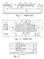
- FIGURES 1 and 2 are representative prior art microbridge MAF structures of this type as disclosed in patent 4,501,144 already cited above.
- the sensors and heater of this prior art device were described as being preferably fabricated of nickel-iron (permalloy) and these sensor and heater grids are encapsulated in a thin film of dielectric, typically comprising layers 28 and 29, preferably of silicon nitride. Air space 30 formed by selective etching of a depression in the monocrystalline silicon base 20 allows the elements 22, 24, and 26 to be surrounded by air. More detail of these prior art figures may be had by reference to patent 4,501,144, the teachings of which are incorporated herein by reference.
- the MAF sensor utilizes the material platinum (in preferred thickness of 1000 angstroms or less) in the fabrication of the resistive elements 22, 24, and 26 although the invention is not in the use of platinum per se.
- platinum is preferred over permalloy.
- the poor adhesion of platinum to silicon nitride is a serious issue in this fabricating process.
- platinum films greater than 4500 angstroms in thickness are said to be adherent to oxide-based ceramics in which the adhesion is said to be dependent on the rough surface of the ceramic, and on the presence of minor constituents in the ceramic, which is never a single compound.
- This roughness is on a scale of many microns up to thousandths of an inch, and would not be suitable for films in the 200 to 3500 angstrom range, for example, for which polished surfaces are required that have no discontinuities due to roughness.
- An objective of this invention is to provide an atomically smooth adhesion layer between the platinum metal sensor layer and the nitride substrate, such that roughness of the interface is not required.
- the layer of this invention must each satisfy two requirements: (1) it must form a strong bond to the platinum and to the silicon nitride, and (2) it must be physically stable against diffusion of its constituent atoms, or any impurities it may contain, into the platinum.
- Standard metallic adhesive films such as Cr or Ti:W alloy can interact with and diffuse into platinum at the elevated annealing temperatures to result in adhesion failure and to severely degrade properties such as TCR and resistance. If no adhesion promoter is used, widespread delamination, blistering and/or agglomeration will result during the necessary high temperature anneal.
- One of the known prior art microstructure gas flow sensors illustrates the limitations which are associated with using a standard chromium (Cr) metal adhesion film with a platinum sensor.
- This prior art device utilizes a chromium adhesion layer of about 50 angstroms beneath the thin film ( ⁇ 1000 angstroms) platinum resistor.
- the annealing temperatures are, of necessity, controlled to less than 400°C to avoid diffusion of chromium into the platinum, whereas platinum is not effectively stabilized with anneals less than about 500°C. If annealing temperatures were to exceed 400°C, a platinum/chromium interdiffusion takes place which severely degrades the platinum sensor properties, for example, by reducing the temperature coefficient of resistance (TCR) to less than half the value obtained by the use of this invention.
- TCR temperature coefficient of resistance
- the adhesion layer must be pure with respect to metallic impurities or excesses of the principal metal. This prevents diffusion of metal atoms from the adhesion layer into the platinum. This stability is particularly important for films of typical thickness of 1000 angstroms because a specified quantity of impurity atoms will have adverse electrical effects after the anneal that are in inverse proportion to the thickness of the platinum film.
- the oxide adhesion layer must be stable, and yet must have surface atoms that bond well to the platinum atoms. However, not all stable oxide layers adhere well. The oxygen surface atoms do not bond well, because platinum oxide is weakly bonded and decomposes at temperatures of the anneal. Therefore, it is the metallic component of the oxide that must form the strong bond.
- SiO2 is a good adhesion layer candidate, because some platinum silicides are stable above the anneal temperatures (PtSi is stable to 1100°C), however, SiO2 is not satisfactory. Si is not a metal, and in the absence of the actual silicide compound, the Pt/Si bond may not be of comparable strength to a Metal/Pt bond of a more generalized type.
- the common factor shared by the satisfactory, preferred metal oxide adhesion layer types is that the metal oxides are quite refractory. That this factor can be a requirement for a successful adhesion layer of this invention is supported by the argument that the oxide must be stable against decomposition which could release metal atoms to contaminate the platinum. We have not investigated all the available metal oxides. However, the following table lists the melting points of the refractory metal oxides which we have found to form adhesion layers which are strongly bonded to and do not contaminate the platinum. It is worthy to note that all of these oxides can be deposited by sputtering reactively in a suitable partial pressure of oxygen to ensure that no excess of metal atoms exists to diffuse into and to contaminate the platinum. metal/oxide melting point (°C) NiO 1984 Ta2O5 1870 Cr2O3 2420 Al2O3 2050
- a thin metal oxide intermediate layer i.e., chromium oxide (Cr2O3), aluminum oxide (Al2O3), tantalum oxide (Ta2O5), nickel oxide (Ni2O3), etc. significantly improves the adhesion of the platinum sensor films on silicon nitride. Incorporation of this adhesion layer also minimizes the development of structural defects and sensor resistance variations which are otherwise encountered.
- One method of fabricating such oxide films makes use of electron beam evaporation of the oxide under high vacuum conditions. We have made satisfactory Al2O3 adhesion layers in this way. This method produces satisfactory adhesion layers, provided that steps are taken to insure correct stoichiometry of the metal oxides. This is necessary to prevent contamination of the platinum by excess metal migrating from the adhesion layer. Using electron beam evaporation, it is generally easier to maintain higher purity of the deposited films relative to sputtering. Purity may be an important consideration when attempting to reproducably obtain a high temperature coefficient of resistance.
- An alternate method is gas discharge sputter deposition with an oxygen component in the discharge gas. With sufficient excess oxygen the complete oxidation of the adhesion layer is assured.
- the following sensor layer processing sequence using sputter deposition is one which can be utilized in the fabrication of Pt sensors with significantly improved adhesion stability.
- RF sputtering as a method utilized for the deposition of the oxide adhesion layers and Pt sensor films.
- Inherent in most sputtering processes is the capability to backsputter, or sputter etch the substrates to remove surface contaminates and/or a thin ( ⁇ 100 ⁇ ) substrate surface layer to provide a clean base material for the subsequent depositions.
- this invention is not limited to the narrow processing area of sputtering, only. Electron beam evaporation, Ion beam deposition, etc., techniques can be utilized to deposit the oxide adhesion layers and Pt sensor films needed in the fabrication of Pt-based sensing devices. In situ substrate cleaning techniques can also be adapted to these other procedures, to provide a clean substrate surface for the subsequent depositions.
- a thin, non-reactive metal oxide (such as Cr2O3, Ta2O5, Ni2O3, and others) adhesion layer in the thickness range of 20 to 100 angstroms, is very effective in enhancing and maintaining platinum adhesion to silicon nitride. This adhesion is continued through the high temperature anneals. Moreover, incorporation of the thin oxide adhesion layer significantly minimizes the development of structural defects and results in markedly improved uniformity and control of platinum sensor/heater resistance properties.
- the oxide adhesion layer does not react with platinum to adversely influence the temperature coefficient of resistance (TCR) or cause undesired changes in resistance.
- TCR temperature coefficient of resistance
- the use of the oxide adhesion layer in the platinum sensor fabrication significantly improves the reliability.
- a silicon substrate 40 having on the surface 41 thereof a thin film of silicon nitride 42.
- the silicon nitride layer may be, for example, on the order of 5000 angstroms in thickness.
- Deposited on the surface 43 of the silicon nitride is a very thin (20-100 angstroms) layer of non-reactive metal oxide 44.
- Chromium (or chromic) oxide (Cr2O3) is one of many effective embodiments of the metal oxide adhesion layer.
- the thin layer of platinum 45 is then deposited over the Cr2O3 adhesion layer. This layer 45 may typically be on the order of 1000 angstroms in thickness, however the thickness may be varied widely depending on the model.
- a surface Cr2O3 adhesion layer 46 is also utilized to promote adhesion between platinum layer 45 and the encapsulation silicon nitride layer 47.
- the incorporation of a thin oxide film not only is an effective adhesion promoter for platinum on silicon nitride, but also minimizes the development of structural defects and the resultant non-uniform resistance which is observed in platinum-only (that is, no adhesion layer) films at elevated temperatures (500-700°C). Also, there are no apparent reactions between the metal oxide adhesion layer and the platinum and the TCR and resistance do not deteriorate as they do when atoms from metal adhesion layers diffuse into the platinum film.
- the thickness of the adhesion layer would not affect its adhesion properties once the thickness exceeded a critical value necessary to completely cover the silicon nitride substrate.
- the critical minimum thickness for good adhesion is about 20 angstroms, with a preferred thickness of about 50 angstroms.
- the 50 angstrom thickness though preferred, is not in any sense a limiting thickness, as other thicknesses will perform well.
- the oxides are reactively sputtered in the static mode from a metal target.
- the oxygen concentration is kept more than high enough to result in fully reacted material.
- Oxides of chromium, aluminum, titanium, tantalum, and nickel were evaluated as adhesion promoting layers for platinum. All oxide films evaluated thus far effectively promote platinum adhesion and permit stabilization and property development anneals at elevated temperatures without deleterious chemical reactions and without the development of defects, delaminations, and uncontrolled resistance shifts that are evident in annealed platinum-only films.
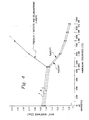
- FIGURE 4 there is shown graphically a plot of the measured sheet resistance vs. annealing temperature for 1000 angstrom platinum films both with and without a metal oxide adhesion layer between the Si3N4 and the platinum film.
- curve A represents the results when platinum is deposited directly on the silicon nitride with no adhesion layer.
- Curve B represents the results when using an adhesion layer of tantalum oxide and Curve C when using an adhesion layer of nickel oxide. It can be seen that the curves track closely with each other at the lower annealing temperatures up to 450°C. Above that temperature, curve A has a discontinuity and breaks sharply upward with defects and delaminations of the platinum occurring. Successful annealing of the platinum with the tantalum oxide and with the nickel oxide adhesion layers was conducted up to 950°C.
Landscapes
- Physics & Mathematics (AREA)
- Engineering & Computer Science (AREA)
- Microelectronics & Electronic Packaging (AREA)
- Fluid Mechanics (AREA)
- General Physics & Mathematics (AREA)
- Electromagnetism (AREA)
- Investigating Or Analyzing Materials By The Use Of Fluid Adsorption Or Reactions (AREA)
- Measuring Oxygen Concentration In Cells (AREA)
- Adhesives Or Adhesive Processes (AREA)
- Electroplating Methods And Accessories (AREA)
- Thermistors And Varistors (AREA)
- Measuring Volume Flow (AREA)
Applications Claiming Priority (2)
| Application Number | Priority Date | Filing Date | Title |
|---|---|---|---|
| US07/289,098 US4952904A (en) | 1988-12-23 | 1988-12-23 | Adhesion layer for platinum based sensors |
| US289098 | 2002-11-06 |
Publications (3)
| Publication Number | Publication Date |
|---|---|
| EP0375399A2 true EP0375399A2 (de) | 1990-06-27 |
| EP0375399A3 EP0375399A3 (en) | 1990-09-19 |
| EP0375399B1 EP0375399B1 (de) | 1995-09-06 |
Family
ID=23110052
Family Applications (1)
| Application Number | Title | Priority Date | Filing Date |
|---|---|---|---|
| EP89313358A Expired - Lifetime EP0375399B1 (de) | 1988-12-23 | 1989-12-20 | Adhäsionsschicht für auf Platin basierende Sensoren |
Country Status (6)
| Country | Link |
|---|---|
| US (1) | US4952904A (de) |
| EP (1) | EP0375399B1 (de) |
| JP (1) | JPH02226017A (de) |
| AT (1) | ATE127583T1 (de) |
| CA (1) | CA2000030A1 (de) |
| DE (1) | DE68924140T2 (de) |
Cited By (13)
| Publication number | Priority date | Publication date | Assignee | Title |
|---|---|---|---|---|
| US5164999A (en) * | 1991-05-20 | 1992-11-17 | Johnson Matthey, Inc. | Blackbody fired on silica fiber |
| US5201022A (en) * | 1991-05-20 | 1993-04-06 | Johnson Matthey Inc. | Coated optical fiber |
| EP0669521A2 (de) * | 1994-02-23 | 1995-08-30 | Honda Giken Kogyo Kabushiki Kaisha | Verfahren zur Herstellung eines Gasstromsensors |
| DE19601592C1 (de) * | 1996-01-18 | 1997-05-07 | Bosch Gmbh Robert | Sensor und Verfahren zur Herstellung eines Sensors |
| DE19605180A1 (de) * | 1996-02-13 | 1997-08-14 | Daimler Benz Ag | Anemometer |
| DE19744228C1 (de) * | 1997-10-07 | 1998-11-26 | Bosch Gmbh Robert | Sensor mit einer Membran |
| AT404758B (de) * | 1993-07-29 | 1999-02-25 | Urban Gerald Dipl Ing Dr | Miniatur-sonde, verfahren zu ihrer herstellung und deren verwendung |
| WO1999041573A1 (de) * | 1998-02-16 | 1999-08-19 | Robert Bosch Gmbh | Sensor in dünnfilmbauweise |
| US6101872A (en) * | 1997-03-14 | 2000-08-15 | Robert Bosch Gmbh | Sensor having a thin film element |
| EP1084392A1 (de) * | 1998-03-16 | 2001-03-21 | UT-Battelle, LLC | Mikromechanische potentiometrische sensoren |
| DE19951595A1 (de) * | 1999-10-27 | 2001-05-17 | Bosch Gmbh Robert | Massenflusssensor mit verbesserter Membranstabilität und einstellbarer Wärmeleitfähigkeit der Membran |
| EP1762851A3 (de) * | 2005-09-07 | 2008-10-22 | Hitachi, Ltd. | Strömungssensor mit Metallfilm-Widerstand |
| WO2017202907A1 (de) | 2016-05-24 | 2017-11-30 | Robert Bosch Gmbh | Verfahren zum herstellen einer elektromigration-resistenten kristallinen übergangsmetall-silizidschicht, entsprechende schichtenfolge und mikro-heizer |
Families Citing this family (57)
| Publication number | Priority date | Publication date | Assignee | Title |
|---|---|---|---|---|
| US5235312A (en) * | 1991-11-18 | 1993-08-10 | Micron Technology, Inc. | Polysilicon resistors and methods of fabrication |
| US5323138A (en) * | 1992-09-04 | 1994-06-21 | Trw Inc. | Reliable thin film resistors for integrated circuit applications |
| US5587130A (en) * | 1993-03-15 | 1996-12-24 | Arizona Board Of Regents | Selected area adhesion and surface passivation of metal films |
| US5468672A (en) * | 1993-06-29 | 1995-11-21 | Raytheon Company | Thin film resistor and method of fabrication |
| US5439840A (en) * | 1993-08-02 | 1995-08-08 | Motorola, Inc. | Method of forming a nonvolatile random access memory capacitor cell having a metal-oxide dielectric |
| US5510013A (en) * | 1993-09-10 | 1996-04-23 | Robert Bosch Gmbh | Layer system for electrochemical probes |
| DE19511590A1 (de) * | 1995-03-29 | 1996-10-02 | Bosch Gmbh Robert | Meßelement für einen Durchflußsensor und Herstellungsverfahren |
| KR100214267B1 (ko) * | 1995-04-07 | 1999-08-02 | 김영환 | 반도체 소자 제조방법 |
| US5759493A (en) * | 1996-04-30 | 1998-06-02 | Arizona Instrument Corporation | Apparatus for detecting a specified gas within a mixture |
| KR100214269B1 (ko) * | 1996-06-27 | 1999-08-02 | 김영환 | 반도체 소자의 보호막 제조방법 |
| US6025205A (en) * | 1997-01-07 | 2000-02-15 | Tong Yang Cement Corporation | Apparatus and methods of forming preferred orientation-controlled platinum films using nitrogen |
| US6054331A (en) * | 1997-01-15 | 2000-04-25 | Tong Yang Cement Corporation | Apparatus and methods of depositing a platinum film with anti-oxidizing function over a substrate |
| JP3457826B2 (ja) * | 1997-01-31 | 2003-10-20 | 株式会社リコー | 薄膜式抵抗体及びその製造方法、流量センサ、湿度センサ、ガスセンサ、温度センサ |
| US5958606A (en) * | 1997-02-05 | 1999-09-28 | Cyntec Company | Substrate structure with adhesive anchoring-seams for securely attaching and boding to a thin film supported thereon |
| US6498097B1 (en) | 1997-05-06 | 2002-12-24 | Tong Yang Cement Corporation | Apparatus and method of forming preferred orientation-controlled platinum film using oxygen |
| US5910880A (en) | 1997-08-20 | 1999-06-08 | Micron Technology, Inc. | Semiconductor circuit components and capacitors |
| US6191443B1 (en) | 1998-02-28 | 2001-02-20 | Micron Technology, Inc. | Capacitors, methods of forming capacitors, and DRAM memory cells |
| US6162744A (en) * | 1998-02-28 | 2000-12-19 | Micron Technology, Inc. | Method of forming capacitors having high-K oxygen containing capacitor dielectric layers, method of processing high-K oxygen containing dielectric layers, method of forming a DRAM cell having having high-K oxygen containing capacitor dielectric layers |
| US6730559B2 (en) * | 1998-04-10 | 2004-05-04 | Micron Technology, Inc. | Capacitors and methods of forming capacitors |
| US6156638A (en) | 1998-04-10 | 2000-12-05 | Micron Technology, Inc. | Integrated circuitry and method of restricting diffusion from one material to another |
| US6165834A (en) * | 1998-05-07 | 2000-12-26 | Micron Technology, Inc. | Method of forming capacitors, method of processing dielectric layers, method of forming a DRAM cell |
| US6255186B1 (en) | 1998-05-21 | 2001-07-03 | Micron Technology, Inc. | Methods of forming integrated circuitry and capacitors having a capacitor electrode having a base and a pair of walls projecting upwardly therefrom |
| JP3606095B2 (ja) * | 1998-10-06 | 2005-01-05 | セイコーエプソン株式会社 | 半導体装置の製造方法 |
| DE19901184C1 (de) * | 1999-01-14 | 2000-10-26 | Sensotherm Temperatursensorik | Platintemperatursensor und Verfahren zur Herstellung desselben |
| DE19901183C2 (de) * | 1999-01-14 | 2001-01-25 | Sensotherm Temperatursensorik | Platintemperatursensor und Herstellungsverfahren für denselben |
| US6369452B1 (en) * | 1999-07-27 | 2002-04-09 | International Business Machines Corporation | Cap attach surface modification for improved adhesion |
| US6331678B1 (en) | 1999-10-29 | 2001-12-18 | Agilent Technologies, Inc. | Reduction of blistering and delamination of high-temperature devices with metal film |
| US7005695B1 (en) | 2000-02-23 | 2006-02-28 | Micron Technology, Inc. | Integrated circuitry including a capacitor with an amorphous and a crystalline high K capacitor dielectric region |
| US7214295B2 (en) * | 2001-04-09 | 2007-05-08 | Vishay Dale Electronics, Inc. | Method for tantalum pentoxide moisture barrier in film resistors |
| JP5138134B2 (ja) * | 2001-07-16 | 2013-02-06 | 株式会社デンソー | 薄膜式センサの製造方法ならびにフローセンサの製造方法 |
| JP4686922B2 (ja) * | 2001-07-19 | 2011-05-25 | 株式会社デンソー | フローセンサの製造方法 |
| EP1622085A1 (de) * | 2004-07-19 | 2006-02-01 | Deutsches Krebsforschungszentrum | Verfahren zur Erzeugung von CT Bildern aus unvollständigen Projektionsdaten eines Untersuchungsobjektes |
| JP5108234B2 (ja) * | 2005-02-07 | 2012-12-26 | 日本特殊陶業株式会社 | マイクロヒータ及びセンサ |
| WO2007091686A1 (ja) * | 2006-02-09 | 2007-08-16 | Mitsui Mining & Smelting Co., Ltd. | 積層体、薄膜センサ、薄膜センサモジュールおよび薄膜センサの製造方法 |
| EP2009647A1 (de) * | 2006-03-28 | 2008-12-31 | Mitsui Mining & Smelting Co., Ltd | Verfahren zum herstellen eines dünnfilmsensors, dünnfilmsensor und dünnfilmsensormodul |
| US7782569B2 (en) * | 2007-01-18 | 2010-08-24 | Sae Magnetics (Hk) Ltd. | Magnetic recording head and media comprising aluminum oxynitride underlayer and a diamond-like carbon overcoat |
| US8014104B2 (en) * | 2007-03-21 | 2011-09-06 | Sae Magnetics (Hk) Ltd. | Magnetic head/disk with transition metal oxynitride adhesion/corrosion barrier and diamond-like carbon overcoat bilayer |
| US8646311B1 (en) | 2007-11-09 | 2014-02-11 | Atmospheric Sensors Ltd. | Sensors for hydrogen, ammonia |
| US8039314B2 (en) * | 2008-08-04 | 2011-10-18 | International Business Machines Corporation | Metal adhesion by induced surface roughness |
| TWI514608B (zh) * | 2010-01-14 | 2015-12-21 | Dow Global Technologies Llc | 具曝露式導電柵格之防溼光伏打裝置 |
| EP2534693A2 (de) * | 2010-02-09 | 2012-12-19 | Dow Global Technologies LLC | Feuchtigkeitsbeständige pv-module mit verbesserter sperrschichthaftung |
| US8356514B2 (en) | 2011-01-13 | 2013-01-22 | Honeywell International Inc. | Sensor with improved thermal stability |
| US9664572B2 (en) * | 2012-11-28 | 2017-05-30 | Seagate Technology Llc | Thin films having large temperature coefficient of resistance and methods of fabricating same |
| DE102013016331A1 (de) | 2013-10-05 | 2015-04-09 | Micronas Gmbh | Schichtsystem |
| DE102013016330A1 (de) | 2013-10-05 | 2015-04-09 | Micronas Gmbh | Schichtsystem |
| US9612146B2 (en) | 2014-02-07 | 2017-04-04 | Honeywell International, Inc. | Airflow sensor with dust reduction |
| RU2583952C1 (ru) * | 2015-01-26 | 2016-05-10 | Открытое акционерное общество "Научно-производственное объединение "ЭРКОН" (ОАО "НПО "ЭРКОН") | Способ изготовления тонкопленочного резистора |
| US10305442B2 (en) * | 2016-01-22 | 2019-05-28 | Qorvo Us, Inc. | Guided wave devices with sensors utilizing embedded electrodes |
| US10938367B2 (en) | 2016-03-31 | 2021-03-02 | Qorvo Us, Inc. | Solidly mounted layer thin film device with grounding layer |
| WO2019168655A1 (en) * | 2018-02-28 | 2019-09-06 | Applied Materials, Inc. | Method for measuring a temperature |
| KR102170210B1 (ko) * | 2018-12-20 | 2020-10-28 | 세종공업 주식회사 | 백금 검지체 센서의 고온 환경 안정화 공정 방법 |
| WO2021081524A2 (en) * | 2019-10-24 | 2021-04-29 | The University Of Louisville Research Foundation, Inc. | Microfabricated differential scanning calorimetry system and methods of use thereof |
| US11835529B1 (en) | 2019-10-24 | 2023-12-05 | University Of Louisville Research Foundation, Inc. | Plasma thermograms for diagnosis and treatment of acute myocardial infarction |
| RU2736630C1 (ru) * | 2020-02-10 | 2020-11-19 | Открытое акционерное общество "Авангард" | Тонкопленочный платиновый терморезистор на стеклянной подложке и способ его изготовления |
| CN112880852B (zh) * | 2021-01-07 | 2023-02-24 | 上海交通大学 | 一种高温铂薄膜电阻温度传感器及其制备方法 |
| WO2023288108A1 (en) * | 2021-07-16 | 2023-01-19 | The University Of Chicago | Biocompatible surface for quantum sensing and methods thereof |
| CN115219056B (zh) * | 2022-07-18 | 2024-09-03 | 山东大学 | 一种快响应且耐高温的薄膜型温度传感器及其制备方法 |
Citations (2)
| Publication number | Priority date | Publication date | Assignee | Title |
|---|---|---|---|---|
| DE3603757A1 (de) * | 1985-02-16 | 1986-08-21 | Nippon Soken, Inc., Nishio, Aichi | Schichtwiderstand fuer eine stroemungsmessvorrichtung |
| GB2181298A (en) * | 1985-09-10 | 1987-04-15 | Sharp Kk | Platinum resistance thermometer and manufacture thereof |
Family Cites Families (5)
| Publication number | Priority date | Publication date | Assignee | Title |
|---|---|---|---|---|
| US4514274A (en) * | 1971-09-16 | 1985-04-30 | Imperial Chemical Industries Plc | Electrode for electrochemical processes |
| US4525223A (en) * | 1978-09-19 | 1985-06-25 | Noboru Tsuya | Method of manufacturing a thin ribbon wafer of semiconductor material |
| US4624137A (en) * | 1981-10-09 | 1986-11-25 | Honeywell Inc. | Semiconductor device |
| US4471405A (en) * | 1981-12-28 | 1984-09-11 | International Business Machines Corporation | Thin film capacitor with a dual bottom electrode structure |
| US4423087A (en) * | 1981-12-28 | 1983-12-27 | International Business Machines Corporation | Thin film capacitor with a dual bottom electrode structure |
-
1988
- 1988-12-23 US US07/289,098 patent/US4952904A/en not_active Expired - Fee Related
-
1989
- 1989-10-02 CA CA002000030A patent/CA2000030A1/en not_active Abandoned
- 1989-12-20 AT AT89313358T patent/ATE127583T1/de active
- 1989-12-20 EP EP89313358A patent/EP0375399B1/de not_active Expired - Lifetime
- 1989-12-20 DE DE68924140T patent/DE68924140T2/de not_active Expired - Fee Related
- 1989-12-22 JP JP1334593A patent/JPH02226017A/ja active Pending
Patent Citations (2)
| Publication number | Priority date | Publication date | Assignee | Title |
|---|---|---|---|---|
| DE3603757A1 (de) * | 1985-02-16 | 1986-08-21 | Nippon Soken, Inc., Nishio, Aichi | Schichtwiderstand fuer eine stroemungsmessvorrichtung |
| GB2181298A (en) * | 1985-09-10 | 1987-04-15 | Sharp Kk | Platinum resistance thermometer and manufacture thereof |
Non-Patent Citations (2)
| Title |
|---|
| I.E.E.E. TRANSACTIONS ON ELECTRON DEVICES, vol. ED-34, no. 12, part I of 2 parts, December 1987, New York, US; O. TABATA et al.: "Monolithic Pressure-Flow Sensor" * |
| I.E.E.E. TRANSACTIONS ON ELECTRON DEVICES. vol. ED-34, no. 12, part 1 of 2 parts, December 1987, New York, US; O. TABATA et al.: "Monolithic Pressure-Flow Sensor". * |
Cited By (22)
| Publication number | Priority date | Publication date | Assignee | Title |
|---|---|---|---|---|
| US5201022A (en) * | 1991-05-20 | 1993-04-06 | Johnson Matthey Inc. | Coated optical fiber |
| US5164999A (en) * | 1991-05-20 | 1992-11-17 | Johnson Matthey, Inc. | Blackbody fired on silica fiber |
| AT404758B (de) * | 1993-07-29 | 1999-02-25 | Urban Gerald Dipl Ing Dr | Miniatur-sonde, verfahren zu ihrer herstellung und deren verwendung |
| EP0669521A2 (de) * | 1994-02-23 | 1995-08-30 | Honda Giken Kogyo Kabushiki Kaisha | Verfahren zur Herstellung eines Gasstromsensors |
| EP0669521A3 (de) * | 1994-02-23 | 1996-07-24 | Honda Motor Co Ltd | Verfahren zur Herstellung eines Gasstromsensors. |
| DE19601592C1 (de) * | 1996-01-18 | 1997-05-07 | Bosch Gmbh Robert | Sensor und Verfahren zur Herstellung eines Sensors |
| US6259350B1 (en) | 1996-01-18 | 2001-07-10 | Robert Bosch Gmbh | Sensor and method for manufacturing a sensor |
| DE19605180A1 (de) * | 1996-02-13 | 1997-08-14 | Daimler Benz Ag | Anemometer |
| US6101872A (en) * | 1997-03-14 | 2000-08-15 | Robert Bosch Gmbh | Sensor having a thin film element |
| DE19744228C1 (de) * | 1997-10-07 | 1998-11-26 | Bosch Gmbh Robert | Sensor mit einer Membran |
| WO1999041573A1 (de) * | 1998-02-16 | 1999-08-19 | Robert Bosch Gmbh | Sensor in dünnfilmbauweise |
| DE19806211A1 (de) * | 1998-02-16 | 1999-08-26 | Bosch Gmbh Robert | Sensor in Dünnfilmbauweise |
| DE19806211C2 (de) * | 1998-02-16 | 2000-11-02 | Bosch Gmbh Robert | Sensor in Dünnfilmbauweise |
| EP1084392A4 (de) * | 1998-03-16 | 2001-06-27 | Ut Battelle Llc | Mikromechanische potentiometrische sensoren |
| EP1084392A1 (de) * | 1998-03-16 | 2001-03-21 | UT-Battelle, LLC | Mikromechanische potentiometrische sensoren |
| DE19951595A1 (de) * | 1999-10-27 | 2001-05-17 | Bosch Gmbh Robert | Massenflusssensor mit verbesserter Membranstabilität und einstellbarer Wärmeleitfähigkeit der Membran |
| EP1762851A3 (de) * | 2005-09-07 | 2008-10-22 | Hitachi, Ltd. | Strömungssensor mit Metallfilm-Widerstand |
| EP2293084A1 (de) * | 2005-09-07 | 2011-03-09 | Hitachi, Ltd. | Strömungssensor mit Metallfilm-Widerstand |
| USRE43660E1 (en) | 2005-09-07 | 2012-09-18 | Hitachi, Ltd. | Flow sensor using a heat element and a resistance temperature detector formed of a metal film |
| WO2017202907A1 (de) | 2016-05-24 | 2017-11-30 | Robert Bosch Gmbh | Verfahren zum herstellen einer elektromigration-resistenten kristallinen übergangsmetall-silizidschicht, entsprechende schichtenfolge und mikro-heizer |
| DE102016208970A1 (de) | 2016-05-24 | 2017-11-30 | Robert Bosch Gmbh | Verfahren zum Herstellen einer Elektromigration-resistenten kristallinen Übergangsmetall-Silizidschicht, entsprechende Schichtenfolge und Mikro-Heizer |
| US11191128B2 (en) | 2016-05-24 | 2021-11-30 | Robert Bosch Gmbh | Method for producing an electromigration-resistant crystalline transition-metal silicide layer, a corresponding layer sequence, and a micro heater |
Also Published As
| Publication number | Publication date |
|---|---|
| EP0375399B1 (de) | 1995-09-06 |
| JPH02226017A (ja) | 1990-09-07 |
| CA2000030A1 (en) | 1990-06-23 |
| DE68924140T2 (de) | 1996-05-09 |
| EP0375399A3 (en) | 1990-09-19 |
| ATE127583T1 (de) | 1995-09-15 |
| DE68924140D1 (de) | 1995-10-12 |
| US4952904A (en) | 1990-08-28 |
Similar Documents
| Publication | Publication Date | Title |
|---|---|---|
| EP0375399B1 (de) | Adhäsionsschicht für auf Platin basierende Sensoren | |
| US5006421A (en) | Metalization systems for heater/sensor elements | |
| JPH0819516B2 (ja) | 薄膜状のアルファTaを形成するための方法および構造 | |
| JP5033421B2 (ja) | 超純粋環境および高腐食環境において使用可能なセンサーとその製造方法 | |
| US4153518A (en) | Method of making a metalized substrate having a thin film barrier layer | |
| US4805296A (en) | Method of manufacturing platinum resistance thermometer | |
| JPH06300649A (ja) | 薄膜歪抵抗材料とその製造方法及び薄膜歪みセンサ | |
| KR100450919B1 (ko) | 센서및그제조방법 | |
| US7545625B2 (en) | Electrode for thin film capacitor devices | |
| US4733290A (en) | Semiconductor device and method of fabrication | |
| US6993828B2 (en) | Method for manufacturing metal thin film resistor | |
| JP3385087B2 (ja) | 基板と一体化されたPt薄膜、それを用いた薄膜ヒータ、温度検出素子およびガスセンサ | |
| JP3542012B2 (ja) | 薄膜ガスセンサ | |
| JP2001057358A (ja) | 薄膜を備えたセンサを製作するための方法 | |
| GB2171252A (en) | A platinum resistor for the measurement of temperature | |
| US4823073A (en) | Sensor for measuring the current or voltage of electrically conductive layers present on a reference substrate | |
| JPH09125228A (ja) | マスク及びこれを用いた誘電体薄膜のパターン形成方法 | |
| KR200156459Y1 (ko) | 엔.티.씨 써미스터 | |
| EP4350313A1 (de) | Dehnungswiderstandsfilm, sensor für physikalische quantitäten und verfahren zur herstellung des dehnungswiderstandsfilms | |
| JPH06213613A (ja) | 歪抵抗材料およびその製造方法および薄膜歪センサ | |
| Arshak et al. | Characterisation of a thin-film/thick-film strain gauge sensor on stainless steel | |
| WO2023058201A1 (ja) | 積層電極、電極付き歪抵抗膜および圧力センサ | |
| JPH0894560A (ja) | 薄膜型ガスセンサー | |
| JP2646246B2 (ja) | ガス感応性溥膜素子の製造方法 | |
| JP2002503805A (ja) | 薄膜設計によるセンサ |
Legal Events
| Date | Code | Title | Description |
|---|---|---|---|
| PUAI | Public reference made under article 153(3) epc to a published international application that has entered the european phase |
Free format text: ORIGINAL CODE: 0009012 |
|
| AK | Designated contracting states |
Kind code of ref document: A2 Designated state(s): AT BE CH DE ES FR GB IT LI NL |
|
| PUAL | Search report despatched |
Free format text: ORIGINAL CODE: 0009013 |
|
| AK | Designated contracting states |
Kind code of ref document: A3 Designated state(s): AT BE CH DE ES FR GB IT LI NL |
|
| 17P | Request for examination filed |
Effective date: 19910318 |
|
| 17Q | First examination report despatched |
Effective date: 19930519 |
|
| GRAA | (expected) grant |
Free format text: ORIGINAL CODE: 0009210 |
|
| AK | Designated contracting states |
Kind code of ref document: B1 Designated state(s): AT BE CH DE ES FR GB IT LI NL |
|
| PG25 | Lapsed in a contracting state [announced via postgrant information from national office to epo] |
Ref country code: IT Free format text: LAPSE BECAUSE OF FAILURE TO SUBMIT A TRANSLATION OF THE DESCRIPTION OR TO PAY THE FEE WITHIN THE PRE;WARNING: LAPSES OF ITALIAN PATENTS WITH EFFECTIVE DATE BEFORE 2007 MAY HAVE OCCURRED AT ANY TIME BEFORE 2007. THE CORRECT EFFECTIVE DATE MAY BE DIFFERENT FROM THE ONE RECORDED.SCRIBED TIME-LIMIT Effective date: 19950906 Ref country code: AT Effective date: 19950906 Ref country code: ES Free format text: THE PATENT HAS BEEN ANNULLED BY A DECISION OF A NATIONAL AUTHORITY Effective date: 19950906 Ref country code: BE Effective date: 19950906 Ref country code: NL Free format text: LAPSE BECAUSE OF NON-PAYMENT OF DUE FEES Effective date: 19950906 |
|
| REF | Corresponds to: |
Ref document number: 127583 Country of ref document: AT Date of ref document: 19950915 Kind code of ref document: T |
|
| PGFP | Annual fee paid to national office [announced via postgrant information from national office to epo] |
Ref country code: FR Payment date: 19950918 Year of fee payment: 7 |
|
| PGFP | Annual fee paid to national office [announced via postgrant information from national office to epo] |
Ref country code: DE Payment date: 19950923 Year of fee payment: 7 |
|
| PGFP | Annual fee paid to national office [announced via postgrant information from national office to epo] |
Ref country code: GB Payment date: 19950926 Year of fee payment: 7 |
|
| REF | Corresponds to: |
Ref document number: 68924140 Country of ref document: DE Date of ref document: 19951012 |
|
| ET | Fr: translation filed | ||
| PGFP | Annual fee paid to national office [announced via postgrant information from national office to epo] |
Ref country code: CH Payment date: 19951231 Year of fee payment: 7 |
|
| NLV1 | Nl: lapsed or annulled due to failure to fulfill the requirements of art. 29p and 29m of the patents act | ||
| REG | Reference to a national code |
Ref country code: CH Ref legal event code: PL |
|
| PLBI | Opposition filed |
Free format text: ORIGINAL CODE: 0009260 |
|
| PLBF | Reply of patent proprietor to notice(s) of opposition |
Free format text: ORIGINAL CODE: EPIDOS OBSO |
|
| 26 | Opposition filed |
Opponent name: ROBERT BOSCH GMBH Effective date: 19960605 |
|
| PG25 | Lapsed in a contracting state [announced via postgrant information from national office to epo] |
Ref country code: GB Effective date: 19961220 |
|
| PG25 | Lapsed in a contracting state [announced via postgrant information from national office to epo] |
Ref country code: LI Free format text: LAPSE BECAUSE OF FAILURE TO SUBMIT A TRANSLATION OF THE DESCRIPTION OR TO PAY THE FEE WITHIN THE PRESCRIBED TIME-LIMIT Effective date: 19961231 Ref country code: CH Free format text: LAPSE BECAUSE OF FAILURE TO SUBMIT A TRANSLATION OF THE DESCRIPTION OR TO PAY THE FEE WITHIN THE PRESCRIBED TIME-LIMIT Effective date: 19961231 |
|
| GBPC | Gb: european patent ceased through non-payment of renewal fee |
Effective date: 19961220 |
|
| PG25 | Lapsed in a contracting state [announced via postgrant information from national office to epo] |
Ref country code: FR Effective date: 19970829 |
|
| PG25 | Lapsed in a contracting state [announced via postgrant information from national office to epo] |
Ref country code: DE Effective date: 19970902 |
|
| REG | Reference to a national code |
Ref country code: FR Ref legal event code: ST |
|
| PLBL | Opposition procedure terminated |
Free format text: ORIGINAL CODE: EPIDOS OPPC |
|
| PLBM | Termination of opposition procedure: date of legal effect published |
Free format text: ORIGINAL CODE: 0009276 |
|
| STAA | Information on the status of an ep patent application or granted ep patent |
Free format text: STATUS: OPPOSITION PROCEDURE CLOSED |
|
| 27C | Opposition proceedings terminated |
Effective date: 20020902 |