EP0372440A2 - Filtre numérique - Google Patents
Filtre numérique Download PDFInfo
- Publication number
- EP0372440A2 EP0372440A2 EP89122275A EP89122275A EP0372440A2 EP 0372440 A2 EP0372440 A2 EP 0372440A2 EP 89122275 A EP89122275 A EP 89122275A EP 89122275 A EP89122275 A EP 89122275A EP 0372440 A2 EP0372440 A2 EP 0372440A2
- Authority
- EP
- European Patent Office
- Prior art keywords
- values
- digital filter
- shift register
- coefficients
- filter according
- Prior art date
- Legal status (The legal status is an assumption and is not a legal conclusion. Google has not performed a legal analysis and makes no representation as to the accuracy of the status listed.)
- Granted
Links
Images

Classifications
-
- H—ELECTRICITY
- H03—ELECTRONIC CIRCUITRY
- H03H—IMPEDANCE NETWORKS, e.g. RESONANT CIRCUITS; RESONATORS
- H03H17/00—Networks using digital techniques
- H03H17/02—Frequency selective networks
-
- H—ELECTRICITY
- H03—ELECTRONIC CIRCUITRY
- H03H—IMPEDANCE NETWORKS, e.g. RESONANT CIRCUITS; RESONATORS
- H03H17/00—Networks using digital techniques
- H03H17/02—Frequency selective networks
- H03H17/0294—Variable filters; Programmable filters
Definitions
- the invention relates to a filter for digitally transmitted message signals.
- Such signals can be used, for example, for the digital transmission of audio information.
- a filter arrangement which can be continuously adapted to changing reception conditions by means of a shift register and a computer.
- the "filtering" message is e.g. from a succession of digitally coded values with 8 bits each and is continuously fed to the shift register.
- the shift register is dimensioned so that e.g. At least 1024 values with 8 bits each can be saved. Taking advantage of this great length of e.g. 1024 values are added to each of these individual values using a computer, e.g. a signal processor calculates a new output value according to predetermined mathematical law. The new output value determined by the computer therefore depends on 1024 individual values. About this length of information, generally also over even longer lengths of e.g.
- the proposed mathematical law can be regarded as constant for each new starting value. After the specified length of e.g. 1024 values or after expiry of even greater lengths e.g. If there are several 1024-bit blocks, the mathematical education law assigned to the filter must be changed to calculate the new output values.
- the calculation is also advantageously carried out serially for the individual output value, whereby by The corresponding basic values are made available in between round trips of the shift register.
- the amount available for calculating the larger length (series) of data is Time a few milliseconds, ie approx. 1000 output values have to be calculated in approx. 1 ms, which in turn means approx. 1000 multiplications (per output value) in 1 ⁇ s.
- the invention is based on the object of specifying a filter arrangement which is practical for consumer receivers and which can be adapted to very rapidly changing reception conditions. This object is achieved by the invention characterized in claim 1. Developments of the invention are described in the subclaims.
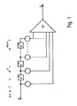
- Figure 1 shows the basic structure of a transversal filter which is suitable for solving the problem described above.
- a shift register 1 is supplied with the data of a digitally coded message signal.
- the output signal is formed by multiplying the individual shift register output signals by certain coefficients (C1 ... Cn) and adding them.
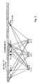
- Fig. 2 shows an embodiment of the invention, in which a serial calculation with only one processor is aimed becomes.
- the fact is used that the multiplications to be carried out for an output value make different contributions to the output value (corresponding to multipliers or coefficients of, for example, 0 to 1). All products are sorted out this principle with a multiplier of 0 in a "pre-process" because they do not contribute to product-sum. The remaining number of values is sorted according to size and limited to a certain, predetermined number of, for example, 50 (out of 1024).
- the circuit in turn contains a memory shift register of appropriate length, e.g. 1024 values of 8 bits each. Since the values to be used for the calculation are now arbitrarily distributed across the register, the relevant values can no longer be made available by pushing the register. This would unnecessarily increase the demands placed on the technology of the shift register.
- the individual shift register cells are therefore connected to a switching matrix (gate network), so that corresponding groups of shift register outputs can be switched through to a corresponding number of outputs of the matrix.
- the switching matrix is controlled with the address sequence determined in the manner described above, it being possible for the sequence for any output value to be arbitrary in the calculation process, because all products are combined to form a sum.
- the 8-bit values are serially assigned to an output of the shift register or the input of the matrix 3, so that a value is transmitted serially.
- the matrix may need to be expanded accordingly.
- FIG. 3 shows how the calculation for several output values is carried out simultaneously.
- the processor works alternately in several summation memories (accumulators). The assignment of the values in the computing process is shown.
- the advantages are that adjacent cells of the shift register can be combined into blocks and can be read out serially by partial revolutions; furthermore, that the multipliers in the processor can be kept constant for the combined value group. For a new value group, the shift register is shifted by a block length.
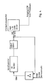
- FIG. 4 shows a further exemplary embodiment in which the function of the memory is taken over by a RAM module (random access memory) with a correspondingly low access time.
- a RAM module random access memory
- an address pre-calculation and control ensure that the required memory contents reach the output.
- the theoretically required address number corresponds to the number of constants (coefficients; 50 in the selected example) multiplied by the number of output values to be calculated in succession for a section with constant coefficients. This would e.g. 2000 output values result in 100,000 addresses to be calculated.
- the I and Q signal with 4PSK demodulation may be used to perform a filtering.
- filtering processes e.g. a so-called Matched filter process and an equalizer process. If the processor's computing capacity permits, the individual processes are combined (I and Q) or, if necessary, executed in succession by the same processor (matched filter and equalizer).
- two memory registers running in parallel must be provided. Calculated intermediate values are to be stored in a buffer, e.g. the output values of the matched filter in order to be able to carry out the equalizer process.
Landscapes
- Physics & Mathematics (AREA)
- Engineering & Computer Science (AREA)
- Computer Hardware Design (AREA)
- Mathematical Physics (AREA)
- Complex Calculations (AREA)
- Oscillators With Electromechanical Resonators (AREA)
- Gasification And Melting Of Waste (AREA)
- Networks Using Active Elements (AREA)
- Compression, Expansion, Code Conversion, And Decoders (AREA)
- Compression Or Coding Systems Of Tv Signals (AREA)
- Reduction Or Emphasis Of Bandwidth Of Signals (AREA)
- Filters That Use Time-Delay Elements (AREA)
- Centrifugal Separators (AREA)
- Dry Shavers And Clippers (AREA)
Applications Claiming Priority (2)
| Application Number | Priority Date | Filing Date | Title |
|---|---|---|---|
| DE3841268A DE3841268A1 (de) | 1988-12-08 | 1988-12-08 | Digitales filter |
| DE3841268 | 1988-12-08 |
Publications (3)
| Publication Number | Publication Date |
|---|---|
| EP0372440A2 true EP0372440A2 (fr) | 1990-06-13 |
| EP0372440A3 EP0372440A3 (en) | 1990-12-27 |
| EP0372440B1 EP0372440B1 (fr) | 1995-02-22 |
Family
ID=6368669
Family Applications (1)
| Application Number | Title | Priority Date | Filing Date |
|---|---|---|---|
| EP89122275A Expired - Lifetime EP0372440B1 (fr) | 1988-12-08 | 1989-12-02 | Filtre numérique |
Country Status (8)
| Country | Link |
|---|---|
| US (1) | US5025406A (fr) |
| EP (1) | EP0372440B1 (fr) |
| JP (1) | JPH02193406A (fr) |
| KR (1) | KR0124367B1 (fr) |
| AT (1) | ATE118929T1 (fr) |
| DE (2) | DE3841268A1 (fr) |
| ES (1) | ES2070885T3 (fr) |
| HK (1) | HK14996A (fr) |
Families Citing this family (3)
| Publication number | Priority date | Publication date | Assignee | Title |
|---|---|---|---|---|
| DE4106928A1 (de) * | 1991-03-05 | 1992-09-10 | Blaupunkt Werke Gmbh | Autoradio |
| FI96256C (fi) * | 1993-04-05 | 1996-05-27 | Tapio Antero Saramaeki | Menetelmä ja järjestely transponoidussa digitaalisessa FIR-suodattimessa binäärisen sisääntulosignaalin kertomiseksi tappikertoimilla sekä menetelmä transponoidun digitaalisen suodattimen suunnittelemiseksi |
| FI97002C (fi) * | 1993-12-17 | 1996-09-25 | Eero Juhani Pajarre | Suora FIR-suodatin, menetelmä pistetulon laskemiseksi FIR-suodattimessa ja menetelmä suoran FIR-suodattimen suunnittelemiseksi |
Citations (1)
| Publication number | Priority date | Publication date | Assignee | Title |
|---|---|---|---|---|
| FR2276635A1 (fr) * | 1974-06-28 | 1976-01-23 | Jeumont Schneider | Multiplieur numerique rapide et ses applications |
Family Cites Families (15)
| Publication number | Priority date | Publication date | Assignee | Title |
|---|---|---|---|---|
| DE270307C (fr) * | ||||
| FR2232153B1 (fr) * | 1973-05-11 | 1976-03-19 | Ibm France | |
| DE2703107A1 (de) * | 1977-01-26 | 1978-07-27 | Siemens Ag | Adaptiver entzerrer |
| DE2703166A1 (de) * | 1977-01-26 | 1978-07-27 | Siemens Ag | Adaptiver entzerrer |
| US4254474A (en) * | 1979-08-02 | 1981-03-03 | Nestor Associates | Information processing system using threshold passive modification |
| US4321686A (en) * | 1980-01-24 | 1982-03-23 | Communications Satellite Corporation | Correction processor of self-adaptive filters |
| US4550415A (en) * | 1983-11-16 | 1985-10-29 | At&T Bell Laboratories | Fractionally spaced equalization using nyquist-rate coefficient updating |
| DE3345284A1 (de) * | 1983-12-14 | 1985-06-27 | Siemens AG, 1000 Berlin und 8000 München | Verfahren und schaltungsanordnung zur digitalsignalverarbeitung nach art eines vorzugsweise adaptiven transversalfilters |
| FR2557746B1 (fr) * | 1983-12-30 | 1986-04-11 | Thomson Csf | Filtre numerique a bande passante et phase variables |
| DE3427349A1 (de) * | 1984-07-25 | 1986-01-30 | ANT Nachrichtentechnik GmbH, 7150 Backnang | Lineares nichtrekursives filter |
| US4843583A (en) * | 1985-10-15 | 1989-06-27 | Rockwell International Corporation | Nonlinear adaptive filter |
| EP0255554B1 (fr) * | 1986-08-07 | 1991-05-08 | Deutsche ITT Industries GmbH | Filtre numérique non récursif |
| US4727424A (en) * | 1986-10-16 | 1988-02-23 | Rca Corporation | Sampled data filtering system, including a crossbar switch matrix, as for a ghost cancellation system |
| GB2197766B (en) * | 1986-11-17 | 1990-07-25 | Sony Corp | Two-dimensional finite impulse response filter arrangements |
| GB8703136D0 (en) * | 1987-02-11 | 1987-03-18 | Univ Cardiff | Filtering electrical signals |
-
1988
- 1988-12-08 DE DE3841268A patent/DE3841268A1/de not_active Withdrawn
-
1989
- 1989-12-02 ES ES89122275T patent/ES2070885T3/es not_active Expired - Lifetime
- 1989-12-02 DE DE58909032T patent/DE58909032D1/de not_active Expired - Fee Related
- 1989-12-02 EP EP89122275A patent/EP0372440B1/fr not_active Expired - Lifetime
- 1989-12-02 AT AT89122275T patent/ATE118929T1/de not_active IP Right Cessation
- 1989-12-07 US US07/447,279 patent/US5025406A/en not_active Expired - Lifetime
- 1989-12-08 JP JP1317942A patent/JPH02193406A/ja active Pending
- 1989-12-08 KR KR1019890018142A patent/KR0124367B1/ko not_active IP Right Cessation
-
1996
- 1996-01-25 HK HK14996A patent/HK14996A/xx not_active IP Right Cessation
Patent Citations (1)
| Publication number | Priority date | Publication date | Assignee | Title |
|---|---|---|---|---|
| FR2276635A1 (fr) * | 1974-06-28 | 1976-01-23 | Jeumont Schneider | Multiplieur numerique rapide et ses applications |
Non-Patent Citations (2)
| Title |
|---|
| N.T.Z.-ARCHIV, Band 7, Nr. 3, M{rz 1985, Seiten 47-57, Berlin, DE; H. G\CKLER: "Einstellbare Digitalfilter f}r die Tontechnik" * |
| TELECOMMUNICATIONS AND RADIO ENGINEERING, Band 39/40, Nr. 8, August 1985, Seiten 93-96, Scripta Technica, Inc., Silver Spring, Maryland, US; S.B. MAKAROV et al.: "Optimizing the structure of nonrecursive digital filter" * |
Also Published As
| Publication number | Publication date |
|---|---|
| KR0124367B1 (ko) | 1997-12-11 |
| ATE118929T1 (de) | 1995-03-15 |
| EP0372440B1 (fr) | 1995-02-22 |
| HK14996A (en) | 1996-02-02 |
| DE3841268A1 (de) | 1990-06-13 |
| DE58909032D1 (de) | 1995-03-30 |
| JPH02193406A (ja) | 1990-07-31 |
| KR900011138A (ko) | 1990-07-11 |
| US5025406A (en) | 1991-06-18 |
| EP0372440A3 (en) | 1990-12-27 |
| ES2070885T3 (es) | 1995-06-16 |
Similar Documents
| Publication | Publication Date | Title |
|---|---|---|
| DE69737416T2 (de) | Adaptiver verteilter entzerrerfilter | |
| DE2329337C2 (de) | "Übertragungsanlage zur Übertragung einer Anzahl Basisbandsignale im Frequenzmultiplex" | |
| DE2451982C2 (fr) | ||
| DE69837299T2 (de) | System und Verfahren zur schnellen Fourier-Transformation | |
| DE2627405B2 (de) | Schaltungsanordnung zur Berechnung der schnellen Fourier-Transformation (FFT) | |
| DD208499A3 (de) | Mehrdimensionaler paralleler speicher | |
| EP0372440B1 (fr) | Filtre numérique | |
| DE2621580C2 (de) | Elektromagnetische oder akustische Empfangseinrichtung mit einer Anzahl von Empfangselementen | |
| DE2163621A1 (de) | Schaltungsanordnung zur Durchführung der Fourier-Analyse | |
| DE3810916A1 (de) | Delta-pulscodemodulation | |
| DE2850718A1 (de) | Sich selbst anpassender entzerrer fuer eine elektrische nachrichtenuebertragungsstrecke | |
| DE69636352T2 (de) | Hierarchische Kodierungs-Vorrichtung und -Verfahren mit Speicher für ein digitales Bildsignal | |
| EP1252725B1 (fr) | Dispositif destine a la mise en oeuvre de procedures de recherche dans un recepteur de telephonie mobile | |
| DE4317869A1 (de) | System zur Bestimmung einer Instabilität in einem IIR-Filter | |
| DE19645057C2 (de) | Vorrichtung zur Selektion von Adressenwörtern mittels Demultiplex-Decodierung | |
| DE2554443C2 (de) | Vorrichtung zur Bildung von Kanälen unter Zuhilfenahme von gleichmäßig auf einer Kreislinie verteilten Detektoren | |
| DE60127126T2 (de) | Realisierung eines digitalen Filters | |
| DE3302885C2 (fr) | ||
| DE2704641A1 (de) | Digitalfilter | |
| DE2724561A1 (de) | Adaptiver entzerrer fuer breitbandige signale | |
| EP0264999A2 (fr) | Système de transmission ou de mémorisation de signaux d'entrée | |
| DE2554430C2 (de) | Vorrichtung zur Bildung von Kanälen unter Zuhilfenahme von gleichmäßig auf einer Kreislinie verteilten Detektoren | |
| DE3223565C2 (fr) | ||
| EP1050143A1 (fr) | Procede pour traiter un signal a base de symboles de donnees | |
| DE102008038780A1 (de) | Frequenzbereichsentzerrer |
Legal Events
| Date | Code | Title | Description |
|---|---|---|---|
| PUAI | Public reference made under article 153(3) epc to a published international application that has entered the european phase |
Free format text: ORIGINAL CODE: 0009012 |
|
| AK | Designated contracting states |
Kind code of ref document: A2 Designated state(s): AT BE CH DE ES FR GB GR IT LI LU NL SE |
|
| PUAL | Search report despatched |
Free format text: ORIGINAL CODE: 0009013 |
|
| AK | Designated contracting states |
Kind code of ref document: A3 Designated state(s): AT BE CH DE ES FR GB GR IT LI LU NL SE |
|
| 17P | Request for examination filed |
Effective date: 19901231 |
|
| 17Q | First examination report despatched |
Effective date: 19931003 |
|
| GRAA | (expected) grant |
Free format text: ORIGINAL CODE: 0009210 |
|
| AK | Designated contracting states |
Kind code of ref document: B1 Designated state(s): AT BE CH DE ES FR GB GR IT LI LU NL SE |
|
| PG25 | Lapsed in a contracting state [announced via postgrant information from national office to epo] |
Ref country code: BE Effective date: 19950222 Ref country code: NL Free format text: LAPSE BECAUSE OF NON-PAYMENT OF DUE FEES Effective date: 19950222 Ref country code: GR Free format text: LAPSE BECAUSE OF FAILURE TO SUBMIT A TRANSLATION OF THE DESCRIPTION OR TO PAY THE FEE WITHIN THE PRESCRIBED TIME-LIMIT Effective date: 19950222 |
|
| REF | Corresponds to: |
Ref document number: 118929 Country of ref document: AT Date of ref document: 19950315 Kind code of ref document: T |
|
| ITF | It: translation for a ep patent filed |
Owner name: BARZANO' E ZANARDO MILANO S.P.A. |
|
| REF | Corresponds to: |
Ref document number: 58909032 Country of ref document: DE Date of ref document: 19950330 |
|
| GBT | Gb: translation of ep patent filed (gb section 77(6)(a)/1977) |
Effective date: 19950324 |
|
| ET | Fr: translation filed | ||
| PG25 | Lapsed in a contracting state [announced via postgrant information from national office to epo] |
Ref country code: SE Effective date: 19950522 |
|
| REG | Reference to a national code |
Ref country code: ES Ref legal event code: FG2A Ref document number: 2070885 Country of ref document: ES Kind code of ref document: T3 |
|
| NLV1 | Nl: lapsed or annulled due to failure to fulfill the requirements of art. 29p and 29m of the patents act | ||
| PG25 | Lapsed in a contracting state [announced via postgrant information from national office to epo] |
Ref country code: AT Effective date: 19951202 |
|
| PG25 | Lapsed in a contracting state [announced via postgrant information from national office to epo] |
Ref country code: LU Free format text: LAPSE BECAUSE OF NON-PAYMENT OF DUE FEES Effective date: 19951231 Ref country code: LI Effective date: 19951231 Ref country code: CH Effective date: 19951231 |
|
| PLBE | No opposition filed within time limit |
Free format text: ORIGINAL CODE: 0009261 |
|
| STAA | Information on the status of an ep patent application or granted ep patent |
Free format text: STATUS: NO OPPOSITION FILED WITHIN TIME LIMIT |
|
| 26N | No opposition filed | ||
| REG | Reference to a national code |
Ref country code: CH Ref legal event code: PL |
|
| REG | Reference to a national code |
Ref country code: GB Ref legal event code: 746 Effective date: 19970904 |
|
| REG | Reference to a national code |
Ref country code: FR Ref legal event code: D6 |
|
| REG | Reference to a national code |
Ref country code: GB Ref legal event code: IF02 |
|
| PGFP | Annual fee paid to national office [announced via postgrant information from national office to epo] |
Ref country code: GB Payment date: 20051110 Year of fee payment: 17 |
|
| PGFP | Annual fee paid to national office [announced via postgrant information from national office to epo] |
Ref country code: DE Payment date: 20051216 Year of fee payment: 17 |
|
| PGFP | Annual fee paid to national office [announced via postgrant information from national office to epo] |
Ref country code: FR Payment date: 20051222 Year of fee payment: 17 |
|
| PGFP | Annual fee paid to national office [announced via postgrant information from national office to epo] |
Ref country code: ES Payment date: 20051227 Year of fee payment: 17 |
|
| PGFP | Annual fee paid to national office [announced via postgrant information from national office to epo] |
Ref country code: IT Payment date: 20061231 Year of fee payment: 18 |
|
| PG25 | Lapsed in a contracting state [announced via postgrant information from national office to epo] |
Ref country code: DE Free format text: LAPSE BECAUSE OF NON-PAYMENT OF DUE FEES Effective date: 20070703 |
|
| GBPC | Gb: european patent ceased through non-payment of renewal fee |
Effective date: 20061202 |
|
| REG | Reference to a national code |
Ref country code: FR Ref legal event code: ST Effective date: 20070831 |
|
| PG25 | Lapsed in a contracting state [announced via postgrant information from national office to epo] |
Ref country code: GB Free format text: LAPSE BECAUSE OF NON-PAYMENT OF DUE FEES Effective date: 20061202 |
|
| REG | Reference to a national code |
Ref country code: ES Ref legal event code: FD2A Effective date: 20061204 |
|
| PG25 | Lapsed in a contracting state [announced via postgrant information from national office to epo] |
Ref country code: ES Free format text: LAPSE BECAUSE OF NON-PAYMENT OF DUE FEES Effective date: 20061204 Ref country code: FR Free format text: LAPSE BECAUSE OF NON-PAYMENT OF DUE FEES Effective date: 20070102 |
|
| PG25 | Lapsed in a contracting state [announced via postgrant information from national office to epo] |
Ref country code: IT Free format text: LAPSE BECAUSE OF NON-PAYMENT OF DUE FEES Effective date: 20071202 |