EP0365618B1 - Circuit de commande electronique, systeme de moteur a commutation electronique et procedes relatifs - Google Patents
Circuit de commande electronique, systeme de moteur a commutation electronique et procedes relatifs Download PDFInfo
- Publication number
- EP0365618B1 EP0365618B1 EP89903554A EP89903554A EP0365618B1 EP 0365618 B1 EP0365618 B1 EP 0365618B1 EP 89903554 A EP89903554 A EP 89903554A EP 89903554 A EP89903554 A EP 89903554A EP 0365618 B1 EP0365618 B1 EP 0365618B1
- Authority
- EP
- European Patent Office
- Prior art keywords
- input
- high voltage
- secondary winding
- inherent
- electronic
- Prior art date
- Legal status (The legal status is an assumption and is not a legal conclusion. Google has not performed a legal analysis and makes no representation as to the accuracy of the status listed.)
- Expired - Lifetime
Links
Images


Classifications
-
- H—ELECTRICITY
- H03—ELECTRONIC CIRCUITRY
- H03K—PULSE TECHNIQUE
- H03K17/00—Electronic switching or gating, i.e. not by contact-making and –breaking
- H03K17/51—Electronic switching or gating, i.e. not by contact-making and –breaking characterised by the components used
- H03K17/56—Electronic switching or gating, i.e. not by contact-making and –breaking characterised by the components used by the use, as active elements, of semiconductor devices
- H03K17/687—Electronic switching or gating, i.e. not by contact-making and –breaking characterised by the components used by the use, as active elements, of semiconductor devices the devices being field-effect transistors
-
- H—ELECTRICITY
- H03—ELECTRONIC CIRCUITRY
- H03K—PULSE TECHNIQUE
- H03K17/00—Electronic switching or gating, i.e. not by contact-making and –breaking
- H03K17/51—Electronic switching or gating, i.e. not by contact-making and –breaking characterised by the components used
- H03K17/56—Electronic switching or gating, i.e. not by contact-making and –breaking characterised by the components used by the use, as active elements, of semiconductor devices
- H03K17/567—Circuits characterised by the use of more than one type of semiconductor device, e.g. BIMOS, composite devices such as IGBT
-
- H—ELECTRICITY
- H02—GENERATION; CONVERSION OR DISTRIBUTION OF ELECTRIC POWER
- H02M—APPARATUS FOR CONVERSION BETWEEN AC AND AC, BETWEEN AC AND DC, OR BETWEEN DC AND DC, AND FOR USE WITH MAINS OR SIMILAR POWER SUPPLY SYSTEMS; CONVERSION OF DC OR AC INPUT POWER INTO SURGE OUTPUT POWER; CONTROL OR REGULATION THEREOF
- H02M7/00—Conversion of ac power input into dc power output; Conversion of dc power input into ac power output
- H02M7/42—Conversion of dc power input into ac power output without possibility of reversal
- H02M7/44—Conversion of dc power input into ac power output without possibility of reversal by static converters
- H02M7/48—Conversion of dc power input into ac power output without possibility of reversal by static converters using discharge tubes with control electrode or semiconductor devices with control electrode
- H02M7/53—Conversion of dc power input into ac power output without possibility of reversal by static converters using discharge tubes with control electrode or semiconductor devices with control electrode using devices of a triode or transistor type requiring continuous application of a control signal
- H02M7/537—Conversion of dc power input into ac power output without possibility of reversal by static converters using discharge tubes with control electrode or semiconductor devices with control electrode using devices of a triode or transistor type requiring continuous application of a control signal using semiconductor devices only, e.g. single switched pulse inverters
- H02M7/5387—Conversion of dc power input into ac power output without possibility of reversal by static converters using discharge tubes with control electrode or semiconductor devices with control electrode using devices of a triode or transistor type requiring continuous application of a control signal using semiconductor devices only, e.g. single switched pulse inverters in a bridge configuration
-
- H—ELECTRICITY
- H02—GENERATION; CONVERSION OR DISTRIBUTION OF ELECTRIC POWER
- H02P—CONTROL OR REGULATION OF ELECTRIC MOTORS, ELECTRIC GENERATORS OR DYNAMO-ELECTRIC CONVERTERS; CONTROLLING TRANSFORMERS, REACTORS OR CHOKE COILS
- H02P6/00—Arrangements for controlling synchronous motors or other dynamo-electric motors using electronic commutation dependent on the rotor position; Electronic commutators therefor
- H02P6/08—Arrangements for controlling the speed or torque of a single motor
- H02P6/085—Arrangements for controlling the speed or torque of a single motor in a bridge configuration
Definitions
- the present invention relates to electronic control circuits, electronically commutated motor systems, and methods for controlling them.
- coassigned Alley U.S. Patent 4,250,544 discloses an arrangement for controlling an electronically commutated motor and is incorporated by reference. Switching of the terminals of winding stages of an electronically commutated motor is accomplished by field effect transistors therein. While such circuitry is effective and satisfactory, it is desirable in some applications contemplated for the electronically commutated motors or in power supplies, to switch relatively high voltages including voltages from generally about 100 volts, for example, up to about 400 volts or more to the winding stages. The terminals thus undergo relatively sudden high voltage excursions relative to the common, or ground connection of the electrical load powering apparatus. Such voltages make the inherent or stray capacitances and inductances of circuits for controlling the switching an important consideration. It is believed that when such higher voltages are used, or whenever the inherent capacitance or inductance is significant, the probability of false triggering, lack of reliable or positive switching, and even oscillation is increased.
- Circuitry with a transformer with numerous windings for base drive of a low input impedance power transistor is illustrated in Mentler U.S. Patents 4,302,807 and 4,308,577. Circuitry with three transformers for input drive of a low input impedance power transistor is shown in Yuzurihara U.S. Patent 4,605,865.
- FETs Field effect transistors
- IGBTs insulated gate transistors
- a power FET driving circuit is described in EP-A-153423 wherein the FET comprises gate, drain and source terminals and an intrinsic capacitance between the gate and source terminals.
- a signal transformer that has an inherent capacitance and inductance that are important considerations; to provide such improved circuits, systems, and methods where a signal transformer is used, to protect from short circuits, transients and other undesired conditions; to provide such improved circuits, systems, and methods where a signal transformer is used, for reliable switching in the presence of a highly inductive load; to provide such improved circuits, systems, and methods where a signal transformer is used, for reliable switching of a solid state power switching device having a high impedance input; to provide such improved circuits, systems, and methods where a signal transformer is used, for higher speed switching of solid state power switching devices; to provide such improved circuits, systems, and methods where a signal transformer is used, for coupling switching waveforms of essentially arbitrarily long or short duration to solid state switching devices; and to provide such improved circuits,
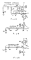
- a system 11 for controlling switching of power supply terminals V+ and V- to a load connection OA has a first solid state power switching device 13 connected between power supply terminal V+ and load connection OA.
- Power switching device 13 has a high impedance input 15 (a gate for instance) and terminals 17 and 19 connected between the V+ terminal and the load connection OA respectively.
- Power switching device 13 is suitably an insulated gate transistor (IGT) having a gate, collector and emitter as shown or a field effect transistor (FET) having a gate, a source and a drain.
- a freewheeling diode 21 is connected with its cathode to terminal V+ and its anode to terminal 19. When a positive potential is applied between terminals 15 and 19 of switching device 13, the device 13 is made conductive and effectively connects terminal V+ to the load connection OA.
- a drive circuit 25 is supplied with a switching waveform AT and correspondingly supplies an electrical control signal between input terminal 15 and load connection OA.
- the switching waveform AT is applied from a separate circuit and for example can be a pulse width modulated (PWM) signal for controlling drive to a load in a regulated power supply or for controlling drive to a brushless motor or other desired load.
- PWM pulse width modulated
- the output of drive circuit 25 is provided as a voltage between terminals 15 and 19 which are subject to high voltage excursions on the order of more than 100 volts or as much as 350-400 volts and more.
- Switching waveform AT is suitably supplied from a separate low voltage integrated circuit which could be adversely affected by high voltage excursions if it were not for circuit 25.
- An additional actuating drive circuit 27 of identical electrical circuit construction as circuit 25 is provided with another different low voltage low frequency PWM waveform AB.
- the output of drive circuit 27 is connected to a power switching device 31 which has a high impedance input terminal 33 and switching terminals 35 and 37.
- Switching terminal 35 is connected to load connection OA and terminal 37 is connected to common and power terminal V-.
- Drive circuit 27 applies a control voltage to terminals 33 and 37 of device 31.
- a free wheeling diode 39 is connected with its cathode to the load connection OA and its anode to terminal 37 of device 31.
- Interference suppressing capacitors 41 and 43 are connected so that capacitor 41 is connected between terminals V+ and V- and capacitor 43 is connected between terminal V- and a chassis or earth ground if one is available.
- Switching device 31 and actuating drive circuit 27 are examples of use of a second solid state power switching device having an input and control terminals connected between the load connection and the common and means connected to the input of the second solid state power switching device for actuating or making conductive the second solid state power switching device.
- Fig. 1 provides a low-cost high-performance DC coupled, isolated, transformer drive circuit for the gate drive of IGTs and FETs to control particularly the upper device in a half-bridge or full bridge power IGT/FET switching control circuit.
- totem pole or half-bridge power converters and inverters When building so-called totem pole or half-bridge power converters and inverters it is useful to provide a level translator which interfaces a low-level control signal, such as AT, to a high voltage level power switching device 13.
- a low-level control signal such as AT
- the gate-source terminals of the power switch are subjected to very rapid excursions from essentially common (ground) to 350-400 volts, for example. This occurs not only due to switching the upper power switch 13 on and off, but also to switching lower device 31 on and off.
- the process of actuating, activating, or otherwise making either device 13 or 31 conductive or of deactuating, deactivating or otherwise making device 13 or 31 nonconductive can introduce these high voltage excursions, level changes or transients.
- the exemplary circuits and methods herein disclosed advantageously account for these high voltage excursions, and allow the input switching waveform (e.g. AT) and only such waveform to control the state of its switching device (e.g. 13) regardless of the transient behavior.
- Inherent non-ideal characteristics of devices and components must be considered in order to provide switching to the load terminal OA in a positive manner which accurately reflects and is controlled by the low frequency control waveforms provided to input connections AT and AB.
- One of these non-ideal characteristics is an input capacitance Cgs of power switching device 13 between its terminals 15 and 19.
- This capacitance typically lies in a range from about 400 picofarads to 1800 picofarads for a typical IGTs which can switch on the order of 50 to 100 amperes with a 15-20 volt gate drive. 5-10 volts of gate drive typically is sufficient for turning on presently available FET power switching devices.
- switching waveform AT is a rectangular pulse on the order of 20 kiloHertz with a pulse length on the order of 10-100 microseconds with about 20 microseconds shown.
- a single pulse of the low frequency control wave form AT is shown having a logic high level for 20 milliseconds and then assuming a logic low level until the high is resumed later. It is applied to a carrier-based switching circuit 41 having two NAND CMOS (complementary metal oxide semiconductor) logic gates 43 and 45 with outputs directly connected to a signal transformer 51 at opposite ends of its primary winding 53. An input terminal from each NAND gate 43 and 45 is connected to receive switching waveform AT.
- CMOS complementary metal oxide semiconductor
- NAND gate 43 An additional input terminal of NAND gate 43 is connected to a clock source providing a square wave clock signal f on the order of 1-5 megaHertz.
- the second NAND gate 45 has an additional input terminal to receive the logical complement of the clock waveform which is designated f/.
- Each NAND gate 43 and 45 is supplied with a low voltage logic level power supply +B, and is alternately enabled by the clock pulses from a clock circuit (not shown), which is of conventional design.
- the clock signal f is a high frequency carrier, suitably in the one (1) megaHertz to five (5) megaHertz range for instance.
- NAND gates 43 and 45 form a pair of gated inverters. That is, when waveform AT is high, the output of NAND gate 43 is f/, the complement of f, and the output of NAND gate 45 is essentially the same as clock signal f.
- the peak-to-peak value of the pulses of Fig. 2B is advantageously twice the CMOS logic level, providing efficient energization of transformer 51.
- the bipolar voltage waveform Vp continues for 20 milliseconds, which is the length of the high pulse of waveform AT of Fig. 2A. Then in Fig. 2B the bipolar waveform ceases until the waveform of Fig. 2A again assumes a logic high level.
- Transformer 51 provides DC isolation between its primary winding 53 and secondary winding 55. Each winding 53 and 55 is suitably wound around the same ferrite magnetizable core with sufficient insulation to easily withstand high voltage on the order of 400 volts and more. Transformer 51 is a non-ideal transformer which exhibits an interwinding capacitance Cw between primary winding 53 and secondary winding 55 as shown in dashed technique. It is to be understood that the interwinding capacitance is more accurately regarded as a capacitance distributed over the entire primary and secondary windings, and it is shown as a single dashed capacitor in Fig. 1 only for convenience of drawing.
- transformer 51 In an example of transformer 51 a 1:1 turns ratio with 15 turns in the primary winding and 15 turns in the secondary winding is utilized and the interwinding capacitance Cw is approximately 5 picofarads. The wire size of the windings is uncritical. Because sufficient insulation must be provided to DC-isolate the primary from the secondary, the magnetic coupling between the primary and secondary is not complete and the primary winding has a self inductance on the order of one millihenry at one megaHertz. This means that the primary draws on the order of 7.5 milliamperes peak current which is well within the capacity of typical complementary metal oxide semiconductor (CMOS) devices for the NAND gates 43 and 45.
- CMOS complementary metal oxide semiconductor
- the voltage across secondary winding 55 of transformer 51 is approximately the same as the primary voltage as shown in Fig. 2B.
- the voltage level of the secondary winding 55 as a whole with respect to common is subject to abrupt changes depending on high voltage excursions at load connection OA, which cause jumps in voltage on the secondary winding 55 between zero volts (common) and a high voltage level due to the switching by power switching devices 13 and 31.
- the voltage of the load connection OA jumps from zero to illustratively 400 volts. Almost concurrently, the voltage level of secondary winding 55 abruptly rises to a high voltage level V Cw of approximately 400 volts due to charging of the inherent interwinding capacitance Cw, while the DC level of primary winding 53 remains near common relatively speaking.
- the interwinding capacitance Cw is charged with the high voltage intentionally from the load connection OA through a pair of serially connected diodes 61 and 63.
- the anode of diode 61 is connected to load connection OA.
- the cathode of diode 61 is connected to the anode of diode 63.
- diodes 61 and 63 act as an example of a means for unidirectional conduction of current between the load connection and the transformer to charge the interwinding capacitance of the transformer when one of the high voltage excursions occurs.
- diodes 61 and 63 constitute an example of first and second means connected at a junction serially for unidirectional conduction through either or both of the first and second means, the first means being connected to the load connection and the second means being connected to the secondary winding to charge the interwinding capacitance when a high voltage excursion occurs at the load connection.
- Diode 63 also is an example of means connected from the secondary winding to the input of an active control means. Diode 63 is poled for unidirectional conduction in a direction opposite to a direction of discharge of current from the inherent interwinding capacitance Cw.
- diodes 67 and 69 are connected across the secondary 55 of transformer 51.
- Diodes 67 and 69 are identically poled with respect to secondary winding 55 and oppositely poled with respect to each other so that their cathodes are connected together at a junction 71 and their anodes are connected to opposite terminals or ends of the secondary winding 55.
- An NPN control transistor 75 has a base connected to the anode of a diode 77 which in turn has its cathode connected to secondary winding 55 at a terminal or end 79 opposite to end 65.
- a voltage V R is developed across a resistor 81 connected between junction 71 of diodes 67 and 69 and a junction 83 of diodes 61 and 63.
- the junction 83 of diodes 61 and 63 is directly connected to the base of transistor 75 and to resistor 81 in this preferred embodiment.
- a value of resistor 81 is typically between 5 and 15 kilohms (K ohms).
- Transistor 75 has its emitter directly connected to load connection OA and has a collector connected to input 15 of switching device 13 by a resistor 87. Also another resistor 89 is connected between input 15 of device 13 and junction 71 of diodes 67 and 69. Resistor 89 is on the order of a few hundred ohms in one preferred embodiment for example, and resistor 87 is on the order of a hundred ohms or less.
- the voltage between junctions 71 and 83 is designated V R .
- the gate voltage between terminals 15 and 19 of device 13 is designated Vg.
- transformer 51 secondary output (same waveshape as in Fig. 2B) is rectified by diodes 67, 69, 63 and 77 (rectified waveform in Fig. 2C) and applied to a resistive network of the hereinabove-described resistors 81, 89 and 87 at first and second connections across resistor 81.
- Resistor 89 is a current limiting resistor which sets the rate of rise of the gate voltage (charging of Cgs). Normally the values of resistor 89 and inherent input capacitance Cgs are selected to allow fast enough turn on of switching device 13 to minimize switching losses, yet slow enough to control electromagnetic interference (EMI) and noise generation.
- EMI electromagnetic interference
- a diode network has at least two diodes and no other elements besides diodes (inherent, stray and insubstantial resistances and reactances excepted), and each diode is connected directly to at least one other diode in the network.
- a resistive network has at least two resistive elements and no other elements besides resistive elements (inherent, stray and insubstantial reactances excepted), and each resistive element is connected directly to at least one other resistive element in the network.
- the diode network and resistive network together act as an example of a means connected to the secondary winding for coupling the pulse output from the secondary winding between the input of the electronic means for switching and the load connection when the pulse output is present.
- a high voltage excursion on the load connection charges the inherent interwinding capacitance to a high voltage level when the pulse output is present.
- Diode 61 also acts as a means responsive to the pulse output of the secondary winding for temporarily preventing or disabling operation of means for bypassing exemplified by transistor 75.
- the circuit 25 of Fig. 1 DC-drives device 13 isolates the drive via transformer 51 and controls the turn-on time and the turn-off time independently for device 13 by resistors 89 and 87 respectively.
- a high noise immunity is necessary for circuit 25 during the rapid voltage changes that occur at the onset of a high voltage excursion at load connection OA and when such an excursion ceases.
- the rate of voltage change at load connection OA is its derivative dv/dt.
- the transformer 51 is efficiently used as a voltage isolation device since it can inexpensively provide isolation for the full amount of the high voltage level to which its inherent input capacitance is charged.
- Charging and discharging or bypassing of capacitance Cw occurs by a flow of current as shown by dashed arrows 113, 121 and 133 of Figs. 3-5.
- This current is termed a common-mode current because it can be allowed to flow in or out of either end 79 or 65 of secondary winding 55, or both ends at once through diodes 67 and 69 to resistors 89 and 87 and through resistor 81 and transistor 75.
- An inherent inductance L of the secondary winding 55 and the resistance R1 of its discharge path also become important factors at the high voltages and higher levels of discharge current.
- the time constant of this discharge path is L/R1, which introduces a degree of delay which is advantageously minimized according to the preferred embodiments and methods of operation by providing a direct resistive path from input lead 15 of device 13 to control transistor 75 to turn the transistor 75 on as soon as possible when waveform AT goes low.
- secondary winding 55 is excluded from the resistive path and prevented from introducing a delay, in turning control transistor 75 on in the first instance.
- transistor 75 and the high impedance input of the switching device 13, but also they provide examples of means for providing between the load connection and both ends of the secondary winding a substantially electrically symmetrical path from the secondary winding to the load connection for bypassing current that is discharging from the inherent interwinding capacitance of the transformer.
- the balance or symmetry considerations just discussed are consistent with the observation that the discharge current is in fact a common mode current, i.e. that it is equally available from both ends of the secondary due to the electrical symmetry of the distributed interwinding capacitance and also of the circuitry with respect to the secondary winding.
- Transistor 75 and resistor 87 effectively bypass the input of device 13 because their low impedance develops relatively little voltage across the input of device 13 when the common mode current 113 is present. In effect input capacitance Cgs is solidly clamped to zero volts relative to the load connection OA.
- diode 61 provides a very low impedance charging path through diodes 63 and 77 directly to both ends 65 and 79 of secondary winding 55 in Fig. 1.
- diode 61 provides a very low impedance charging path through diodes 277 and 279 directly to both ends of the secondary winding of transformer 255.
- diode 61 provides a very low impedance charging path directly to the center tap 257 of the transformer.
- Fig. 9 diode 61 provides a very low impedance charging path directly to the center tap 257 of the transformer.
- diode 61 provides a very low impedance charging path through diode 291 directly to end 289 of the secondary winding of the transformer.
- diode 61 provides a very low impedance charging path directly to end 321 of the transformer.
- diode 61 alone or with one or more other diodes effectively and advantageously acts as an example of further means for bypassing the high impedance input of the switching device when the inherent interwinding capacitance of the secondary winding is being charged when a high voltage excursion occurs and for preventing the switching device from being turned off when a high voltage excursion occurs.
- the diode network, resistive network and active control means such as transistor 75 act as as an example of a means for isolating the high impedance input of the switching device from any substantial transient potential differences due to inherent energy storage parameters of the transformer and of the switching device when each high voltage excursion occurs and when each high voltage excursion ceases thereby to prevent the switching device from being spuriously changed in its state of nonconduction or conduction when a high voltage excursion occurs and ceases respectively.
- the switching device is caused to faithfully reflect the state of a switching waveform (e.g. AT) in its state of nonconduction or conduction.
- AT switching waveform
- the preferred embodiments in the Figures each act as a total drive system which automatically rejects the potentially troublesome interwinding capacitance of the signal transformer (e.g. 51, 255, 285 or 311 in the various Figures) thus allowing fast switching of devices 13 and 31.
- the signal transformer is small and economical, with an uncomplicated two-winding arrangement, and thus compatible with the high carrier frequency of the clock pulses f.
- the primary winding is solely associated with a single secondary winding and no additional windings are needed in the embodiments shown. Low cost winding methods are feasible because potentially troublesome transient behavior due to the inherent interwinding capacitance is bypassed, compensated, balanced, offset and obviated.
- Control transistor 75 is an NPN transistor with an emitter connected to the load connection, a collector resistively connected to the input of the electronic means, and a base as a suitable input of active control means connected also to sense the high voltage level on the inherent interwinding capacitance.
- transistor 75 is an inexpensive low power device that need only conduct 50-100 milliamperes peak current, for one example.
- the transistor 75 is rendered conductive by a predetermined polarity referenced to the load connection rather than referenced to the input 15 of the switching device 13.
- a junction field effect transistor (JFET) or other active solid state device can be used as an active control means instead of an NPN transistor according to the principles discussed.
- Control transistor 75 constitutes an example of active device means having a first electrode directly and ohmically connected to the load connection, a second electrode connected to the junction of first and second means for unidirectional conduction and a third electrode resistively connected to the second electrode and resistively connected to the input terminal of a high impedance input switching device.
- the active control means exemplified by transistor 75 is only responsive to a predetermined voltage polarity between its input and the first control lead.
- the secondary winding is connected between the input and the second control lead of the active control means so that the pulse output is prevented from actuating the active control means (i.e., from making it conductive) and is coupled instead to the electronic means for switching.
- Diode 61 acts as a unidirectional conduction means connected between the load connection and the input of the active control means and poled to develop a disabling voltage opposite to the predetermined voltage polarity when a high voltage excursion occurs.
- Resistors 89 and 81 together with resistor 87 and control transistor 75 constitute an example of a means for providing an essentially delay free path from the inherent capacitance of high impedance input switching means to the active control means at a second electrode so that when a normal output across the secondary winding ceases both the inherent capacitance of the high impedance input switching means and the interwinding capacitance of the transformer means are discharged and the high impedance control device positively switches.
- resistors 89 and 81 together with resistor 87 and control transistor 75 constitute an example of a means for bypassing the high voltage level on the inherent interwinding capacitance of the transformer to the load connection when the pulse output and each high voltage excursion cease, including active control means having an input and first and second control leads and means for providing a resistive path substantially free of inductance between the input of the active control means and the input of the electronic means, the active control means thereby bypassing current from the input of the electronic means to the load connection through the first and second control leads and the high voltage level being prevented from actuating the electronic means when each high voltage excursion ceases.
- the resistive network when one of the output pulses from the diode network ceases, provides an essentially delay-free direct path from the high impedance input of the solid state power switching device to the active control means and the inherent input capacitance is discharged through the active control means.
- the inherent input capacitance is discharged through at least two of the control leads of the active control means, turning the switching device off, and when the high voltage excursion ceases the inherent interwinding capacitance is thereby also bypassed through the active control means, and the high impedance input of the solid state power switching device is thus fully bypassed.
- Diodes 67, 69, 63 and 77 of Fig. 1 also can be viewed as a full wave bridge rectifier or rectification means connected across the secondary winding 55.
- the rectification means has a first output (e.g. at junction 83) connected directly to the base input of active control means, and a second output (e.g. at junction 71) connected to the resistive network.
- the active control means has its input and at least one of its control leads directly connected to the resistive network (e.g. to resistors 81 and 87 respectively).
- the resistive network has a further connection for the input 15 of the electronic means for switching (e.g. device 13).
- the bipolar voltage of Fig. 2B is full wave rectified to produce a series of very high frequency pulses that as full wave rectified very nearly approximate a continuous low frequency DC voltage pulse like that shown in Fig. 2A, recovering same.
- the full wave rectified voltage of Fig. 2C appears as voltage V R and is applied through resistor 89 to the high impedance input terminal 15 of switching device 13.
- the series resistance substantially provided by resistor 89 together with the input capacitance Cgs of device 13 provide an RC charging waveform on the leading edge of the gate voltage Vg of Fig.
- control transistor 75 is immediately turned on and maintained on in an effectively delay-free manner due to the voltage Vg on the inherent capacitance Cgs of device 13 discharging through resistor 89 through resistor 81 and into the base emitter path of control transistor 75.
- there is no delaying element such as a series inductance or a parallel capacitance interposed between the inherent capacitance Cgs of device 13 and the discharge network constituted by resistors 81, 89 and 87 together with control transistor 75.
- the secondary winding of transformer 51 is independent of and excluded from the discharge path from the gate lead 15 to the load connection through transistor 75.
- the diodes of the full wave rectifying circuit 67, 69, 77 and 63 prevent the discharge of current from the gate of device 13 into the secondary winding 55.
- control transistor 75 rapidly and effectively bypasses the input capacitance Cgs of device 13 preventing inadvertent energization of device 13 after the control voltage at point AT has ceased in Fig. 2A. Therefore in Fig. 2D the very rapid and steep discharge curve is executed which effectively and positively terminates the gate voltage Vg at the high impedance input of device 13 thereby turning device 13 off.
- Fig. 3 shows this effective and advantageous discharge and bypassing process which is importantly provided by the embodiment of Fig. 1.
- Load connection OA is initially at 400 volts when power switching device 13 is turned from on to off. Regardless of the state of conduction of device 31 freewheeling diode 39 conducts if the load such as an electronically commutated motor 101 is inductive. In such case a winding stage 103 (by the inductive fly-wheel effect) attempts to maintain the load current flowing in winding stage 103 which then is conducted to either or both of winding stages 105 and 107 in the Y-connected electronically commutated motor 101. Diode 39 is conducting, so the voltage of load connection OA is one diode drop below common.
- the input capacitance of device 13 discharges to the load connection as shown by arrow 111, through resistor 87 and the transistor 75.
- the interwinding capacitance Cw is simultaneously discharged as shown by an arrow 113 through forward conducting diode 67 (as well as 69).
- Part of the Cw discharge current passes through base resistor 81 thence into the base of control transistor 75 and out the emitter of control transistor 75 to the load connection OA and to common.
- Most of the Cw discharge current passes through resistors 89 and 87 and thence through transistor 75 to the load connection and to common.
- a discharge current Id from interwinding capacitance Cw through resistance R of the bypassing circuit comprised of resistor 87 and transistor 81 collector-emitter path should be less than a current value that develops voltage Vto.
- the product RId should be less than Vto.
- soldving for resistance R yields the inequality that R should be less than the ratio Vto/(dv/dt Cw) as a bypassing condition.
- the skilled worker selects the appropriate component values to achieve the bypassing effect.
- a resistance 87 value of 100 ohms or less is satisfactory for bypassing FETs and IGTs.
- the voltage derivative dv/dt is related to the load inductance, maximum load current and interelectrode capacitances of the power switch 13, among other variables, and suitably is measured or estimated for the particular application.
- a typical value of the voltage derivative is 4 volts per nanosecond.
- Fig. 4 a charging mode of the circuit of Fig. 1 is illustrated.
- Power switching device 13 switches from off to on.
- Current flows from the high voltage terminal V+ of an external power source through power switching device 13 into winding 103 of the Y-connected electronically commutated motor 101.
- Load connection OA suddenly rises to 400 volts for example and a charging current 121 shown by a dashed line also simultaneously flows through the serially connected unidirectional conduction diodes 61 and 63 (and 77).
- Figs. 3-5 are simplified to illustrate the action of drive circuit 25 of Fig. 1 with inactive or nonconducting devices for the most part being omitted for clarity to more effectively illustrate the modes of a preferred embodiment of the invention in different phases of its operation.
- Fig. 5 illustrates a still further mode by which the interwinding capacitance Cw is charged through the two unidirectional conduction devices 61 and 63 even though the upper power switching device 13 is off at the time.
- the lower switching device 31 has been on and is suddenly switched off.
- the inductance of winding 103 in the load for example has been flowing toward load terminal OA. Because of the flywheel effect of the inductance of winding 103 it acts to keep the current flowing.
- the voltage at load terminal OA suddenly rises in an abrupt high voltage excursion so that current 131 flows upward through freewheeling diode 21 into the positive high voltage terminal V+ thereby returning energy to the power supply.
- Power switching device 13 is off at this time. Because of the sudden rise in voltage however a charging current 133 as shown by a dashed line also flows from the high voltage terminal OA through diode 61 and diode 63 (and 77) into the interwinding capacitance C w .
- Fig. 6 shows an example of less preferable operation of an alternative apparatus which has a transformer drive circuit 141 for the power switching device 13 and the motor windings 103, 105 and 107.
- a PNP transistor 143 has its emitter connected to the high impedance input 15 of power switching device 13.
- the collector of PNP transistor 143 is connected by a resistor 145 to the load connection OA.
- a diode 147 has its cathode connected to the emitter of transistor 143 and its anode connected to the base of transistor 143.
- the inherent interwinding capacitance Cw of a transformer (not shown) is connected through a diode 149 and a resistor 151 in series to the base of transistor 143.
- a resistor 153 connects diode 149 cathode to the load connection OA.
- Fig. 7 shows a preferred embodiment of an electronically commutated motor system. All of the circuitry of Fig. 1 (circuits 25 and 27 and the power switching devices 13 and 31 and diodes 21 and 39) is regarded as a drive A of Fig. 7.
- circuit 27 includes a second transformer having a primary winding and a secondary winding for providing at least one pulse output, and means for coupling the pulse output from the secondary winding of the second transformer between the input of a second solid state power switching device and common.
- the electronic control circuit further includes clock circuit means for producing pulses having a repetition rate and first and second means for switching the pulses at a switching rate less than the repetition rate to the primary windings of the first and second transformers (e.g. of circuits 25 and 27 respectively) in accordance with first and second switching waveforms respectively.
- FIG. 7 three duplicates of all of the circuitry in Fig. 1 are provided as drives A, B and C of Fig. 7.
- the load connection designated OA in Fig. 1 is identically marked as terminal OA for drive A of Fig. 7.
- Load connections of the identical circuitry of drive B and drive C are correspondingly marked as load connections OB and OC.
- Load connections OA, OB and OC are connected to the winding stage terminals of Y-connected electronically commutated motor 101 of Fig. 7.
- Motor 101 illustratively drives an 8.5 horsepower compressor 151.
- Compressor 151 supplies refrigerant at a high side pressure to a condenser 153 which then feeds a thermal expansion valve (TEV) 155 that in turn supplies an evaporator 157 which returns the refrigerant to compressor 151.
- TSV thermal expansion valve
- Electronically commutated motor 101 includes a stationary assembly having a plurality of winding stages adapted to be selectively commutated, and rotatable means associated with the stationary assembly in selective magnetic coupling relation with the winding stages, as described in coassigned U.S. patent 4,528,485 incorporated by reference herein, for example.
- Motor 101 is commutated by circuitry for commutating the winding stages by selectively switching the winding stages at the respective terminals OA, OB and OC thereof to the high voltage connection V+ in response to command pulses.
- the drive A of Fig. 7 has two inputs AT and AB for the top and bottom A inputs corresponding to Fig. 1. These are supplied by a motor controller 161 which has top and bottom outputs not only for drive A (AT, AB) but also drive B (BT, BB) and drive C (CT, CB). These outputs are provided in the manner of the above cited Bitting et al. U.S. patent 4,500,821 which is incorporated herein by reference.
- the motor controller utilizes back EMF position sensing from the terminals of the Y-connected electronically commutated motor 101.
- Sensing circuits 171, 173 and 175 for drives A, B and C respectively are connected to the winding stage terminals OA, OB and OC as voltage dividers with low side RF bypass condensers to produce position sensing voltages VA, VB and VC respectively that are returned to corresponding inputs of motor controller 161.
- Sensing circuits 171, 173 and 175 and motor controller 161 act as respective examples of position sensing means for producing electrical position signals representing the position of the rotatable means, and means for generating the command pulses in response to the electrical position signals from the position sensing means.
- the motor system electronics includes solid state power switching devices each having a high impedance input and control terminals connected between the high voltage supply connection and the terminals of the winding stages respectively.
- transformers respectively correspond to each of the solid state power switching devices.
- Each of the transformers has a primary winding and a secondary winding for providing an output from the secondary winding in response to a respective one of the command pulses, and an inherent interwinding capacitance is present between the primary winding and the secondary winding.
- Circuitry connected to each secondary winding couples the output from each secondary winding between the high impedance input of each solid state power switching device and the terminal of the winding stage to which the switching device is connected.
- Active control means each have an input and first and second control leads and circuitry provides resistive paths substantially free of inductance between the input of each active control means and the high impedance input of each of the solid state power switching devices respectively.
- the active control means are connected to bypass the high voltage level on each inherent interwinding capacitance thus charged thereby to bypass the high voltage level from the high impedance input of the corresponding solid state power switching device to the terminal of the corresponding winding stage through the first and second control leads when each high voltage excursion ceases. In this way, the high voltage level is prevented from actuating any of the solid state power switching devices when each high voltage excursion ceases.
- This electronically commutated motor system of Fig. 7 is suitable for refrigeration, air conditioning, heat pump and other heat transfer or other applications requiring economic and reliable drive. It is contemplated that the electronically commutated motor systems of the present invention may also be applied in all applications to which their advantages commend them, such as automotive applications, household and industrial applications, including fluid transfer applications such as heat transfer or refrigeration systems and air moving fan motors, automotive blower motors and other applications too numerous to specifically detail.
- a switching regulator power supply 201 has identical drives designated Drive A and Drive B, each of which are identical to the circuitry shown in Fig. 1, are connected with their load connections OA and OB connected to opposite sides of a first winding 203.1 of a power transformer 203 of the switching regulator.
- a low voltage second winding 203.2 of the switching regulator feeds a rectifier and filter circuit 205 of conventional full wave rectifier and capacitive filter type, for example.
- Circuit 205 is an example of a means connected to the output winding of the power transformer for deriving an output voltage of the switching regulator power supply.
- the output of circuit 205 is connected to terminals at which the regulated DC supply voltage output of the power supply is made available.
- Error detector 207 is an example of a means for detecting a difference between the output voltage and a predetermined value to which the output voltage is to be regulated. (Ground triangle symbols marked with a "2" inside them indicate an output common which is DC-isolated (by optocoupling for instance) from the drive commons shown as unmarked ground triangle symbols.)
- the output of PWM circuit 209 produces pulses of variable width 211 and 213 on corresponding lines 221 and 223.
- PWM circuit 209 is an example of a means for generating a pulse width modulated series of pulses for energizing the primary winding of the signal transformer (e.g. transformer 51 of Fig.
- Lines 221 and 223 are connected to the inputs AT and AB respectively of drive A and to inputs BB and BT respectively of drive B so that drive A and drive B alternately energize their load connections to drive the power transformer 203 with a bipolar voltage.
- the energy for drives A and B is supplied by a full wave rectifier bridge 231 which obtains power from commercial mains through plug 233 and supplies high voltage supply terminals V+ and V- of each of drives A and B.
- Capacitive filtering is provided by a capacitor 233.
- a one megaHertz clock circuit 241 of conventional construction provides outputs f and f/ to corresponding inputs of drive A and drive B.
- the clock circuit is an example of a clock circuit means for producing pulses having a repetition rate and the NAND gates 43 and 45 of Fig. 1 together are an example of a means for switching the pulses at a switching rate less than the repetition rate to the primary windings of signal transformers in drives A and B in response to PWM circuit 209.
- a low voltage power supply subsection 245 has a voltage dropping resistor 247, 15 volt Zener diode 249 and filter capacitor 251 to provide a nominally +15 volt logic supply to terminals +B of drive A and drive B.
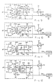
- Figs. 9-12 illustrate some additional embodiments of drive circuitry which can be substituted for drive circuit 25 of Fig. 1. Corresponding devices in each of these Figs. 9-12 which are unchanged compared to Fig. 1 are maintained with corresponding reference numerals.
- NAND gates 43 and 45 feed the primary winding of a transformer 255 having a two to one turns ratio between secondary and primary.
- the secondary winding is center tapped at a center tap 257.
- Center tap 257 is connected directly to the junction of resistor 81, cathode of diode 61 and base of control NPN control transistor 75.
- Ends 261 and 263 of the secondary winding of transformer 255 are connected to the anodes of diodes 267 and 269 respectively.
- the cathodes of diodes 261 and 269 are connected together to the junction of resistors 81 and 89 and produce a full wave rectified voltage V R as shown in Fig. 2C to essentially recover the switching waveform AT of Fig. 2A.
- the circuit of Fig. 9 advantageously provides a direct delay-free path from the high impedance input of switching device 13 through resistors 89, 81 and 87 through control transistor 75 to the load connection OA.
- An inherent interwinding capacitance 271 distributed across the windings of transformer 255 is discharged in a balanced symmetrical manner through the base of control transistor 75 as well as through diodes 269 and 267 to efficiently and very rapidly discharge the interwinding capacitance when necessary.
- the interwinding capacitance is charged from load connection OA through diode 61 which has its cathode directly connected to center tap 257.
- the full wave rectification is accomplished with the same transformer 255 except that the center tap 257 is connected to the junction of resistors 81 and 89.
- the secondary winding has a tap directly connected to means for providing an essentially delay-free path such as a passive and resistive electrical network at a point electrically distinct from the second control lead of the active control means.
- the ends 261 and 263 of the secondary winding are in this embodiment connected to the cathodes of two diodes 277 and 279.
- the anodes of both identically poled diodes 277 and 279 are both connected to the cathode of diode 61 and to the base of control transistor 75.
- NAND gates 43 and 45 are connected to the primary winding of a transformer 285 which has more turns in its secondary than in its primary.
- One end 287 of the secondary winding is connected to the junction of resistors 81 and 89 and another end 289 of the secondary winding of transformer 285 is connected to the cathode of a diode 291 the anode of which is serially connected with the cathode of diode 61 at a junction.
- the junction between diode 61 and diode 291 is directly connected to the base of transistor 75.
- a capacitor 295 of approximately 100 picofarads in value is connected between end 287 of the secondary winding and the base of control transistor 75.
- Diode 291 and capacitor 295 form a half wave rectifier and filter with sufficient filtering to drive and hold power switching device 13 on between adjacent half cycles of the one megaHertz clock pulses.
- Capacitor 295 also acts as a speedup capacitor for discharging and bypassing purposes.
- the secondary wading is capacitively connected to the input of the active control means and the input of the active control means is also separately connected to the secondary winding to sense the high voltage level on the inherent interwinding capacitance.
- NAND gates 43 and 45 have their outputs connected to the bases of four driver transistors 301, 303, 305 and 307.
- NAND gate 43 output is connected to the bases of driver transistors 301 and 303.
- NAND gate 45 output is connected to the bases of driver transistors 305 and 307.
- the emitters of transistors 301 and 303 are connected to a first side of a primary of a transformer 311 and the emitters of transistors 305 and 307 are both connected to the opposite side of the primary.
- the collectors of transistors 301 and 307 are both connected to 15 volts +B low voltage supply.
- the secondary winding of transformer 311 has approximately twice as many turns as the primary winding of the transformer and a secondary terminal 317 is connected to the anode of a diode 319 the cathod of which is connected to the junction of resistors 81 and 89.
- a capacitor 323 of approximately 100 picofarads value is connected between the cathode of diode 319 and the opposite terminal 321 of the secondary winding of transformer 311.
- the base of control transistor 75 and the cathode of the diode 61 are together connected directly to the secondary winding terminal 321. Otherwise the connections of resistors 81, 89 and 87 and control transistor 75 and switching device 13 are the same as those in Fig. 9.
- a capacitor analogous to capacitor 295 of Fig. 11 is advantageously connected across resistor 81 in Figs. 1, 9 and 10. This capacitor even further removes the ripple and notches in Figs. 2C and 2D and provides a speedup capacitor action for discharge and bypassing purposes. Also, use of such capacitor permits some savings in transformer 51 of Figs. 9 and 10, which can have less perfectly balanced and less tightly coupled halves provided in its secondary winding. In addition, the capacitor eliminates noise interference which could be magnetically induced into the higher impedance of resistor 81 from any nearby high-current conductor which might be present in the load or on a printed circuit or in other circuitry of a particular application.
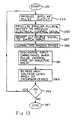
- Fig. 13 shows steps of some preferred methods of operating the control circuitry, electronically commutated motor system and switching regulator power supply of the earlier Figures.
- Fig. 13 operations begin at a START 351 and proceed to a step 353 to produce a bipolar pulse output from a transformer having a primary winding and a secondary winding with an inherent interwinding capacitance between the primary winding and the secondary winding.
- the bipolar pulses are processed, such as through a diode network, so that they are rectified to produce or recover an electrical control signal.
- the bipolar pulse output thus processed to produce the electrical control signal is resistively coupled between the high impedance input of a solid state switching device and the load connection. This operation charges the inherent input capacitance of the solid state switching device, switching it on. At this time a high voltage excursion on the load connection charges the inherent interwinding capacitance of the transformer to a high voltage level.
- the winding stages are commutated.
- the switching regulator power supply of Fig. 8 the first winding 203.1 of the power transformer 203 acts as a single winding stage.
- the three winding stages of the motor 101 are commutated by selectively switching the winding stages at respective terminals thereof to the high voltage connection with high impedance input solid state switching devices in response to pulses.
- step 361 the input capacitance of each solid state switching device which is turned off by commutation is discharged substantially free of inductive delay, when the bipolar pulses so rectified cease to produce the electrical control signal.
- a further step 363 bypasses the high voltage level on the interwinding capacitance of the transformer when each high voltage excursion on the load connection ceases, to bypass the high impedance input of the electronic means for switching when each high voltage excursion ceases.
- each interwinding capacitance thus charged is bypassed to the terminal of the corresponding winding stage to avoid actuating the high impedance input of each corresponding solid state power switching device when each high voltage excursion ceases.
- an electrical signal representing the charged input capacitance of each solid state switching device is provided substantially free of inductive delay from the input of the switching device to an active control means so that the active control means bypasses current from the input of the switching device to the load connection and the high voltage level is prevented from actuating the electronic means when each high voltage excursion ceases.
- each interwinding capacitance is bypassed to avoid activating the high impedance input of each corresponding solid state power switching device when each high voltage excursion ceases.
Abstract
Claims (22)
- Circuit de commande électronique utilisable avec un appareil d'alimentation d'une charge électrique ayant une borne de connexion de charge (OA), une borne d'alimentation tension élevée et une borne de référence commune, et avec des moyens électroniques (13, 31) pour relier par commutation la borne d'alimentation de tension élevée vers la borne de connexion de charge (OA), les moyens électroniques (13, 31) ayant une entrée (15, 33) et réagissant à une différence de tension entre l'entrée (15) et la borne de connexion de charge soumise à des fortes excursions de tension relativement à la borne de référence en raison de la commutation, comprenant :
un transformateur (51) ayant un enroulement primaire (53) et un enroulement secondaire (55) pour fournir au moins une sortie impulsionnelle à partir de l'enroulement secondaire, ce transformateur ayant une capacité de couplage propre (Cw) entre l'enroulement primaire et l'enroulement secondaire,
des moyens de redressement (63, 67, 69, 77) connectés à l'enroulement secondaire pour coupler la sortie impulsionnelle de l'enroulement secondaire entre l'entrée (15) des moyens électroniques (13) et la borne de connexion de charge (OA) en présence d'une impulsion de sortie, une forte excursion de tension au niveau de la borne de connexion de charge chargeant la capacité de couplage propre à un niveau de tension élevée en présence d'une impulsion de sortie,
des moyens (61, 75) pour dériver le niveau de tension élevé de la capacité de couplage propre (Cw) du transformateur (51) vers la borne de connexion charge (OA) à la disparition de l'impulsion de sortie et de chaque forte excursion de tension, et
des moyens de commande actifs (75) ayant une entrée et des premier et deuxième fils de commande et des moyens (81, 89) pour fournir un chemin résistif sensiblement non inductif entre l'entrée des moyens de commande actifs (75) et la sortie (15) des moyens électroniques (13, 31), et des moyens de commande (61) pour commander la conduction des moyens de commande actifs (75) en réponse à un courant de décharge de la capacité de couplage propre et l'état de non-conduction des moyens de commande actifs (75) en réponse à un courant de charge de la capacité de couplage propre, les moyens de commande actif étant connectés pour dériver le courant de l'entrée (15) des moyens électroniques (13) vers la borne de connexion de charge (OA) par l'intermédiaire des premier et deuxième fils de commande, ce qui empêche le niveau de tension élevée de la capacité de couplage propre (Cw) d'activer les moyens électroniques (13, 31) à la disparition de chaque forte excursion de tension. - Circuit de contrôle électronique selon la revendication 1, caractérisé par le fait que les moyens pour fournir un chemin résistif comporte un réseau résistif (81, 89) et lesdits moyens de couplage comportent des moyens de redressement en pont à double alternance (63, 67, 69, 77) connectés aux bornes de l'enroulement secondaire (55), lesdits moyens de redressement en pont à double alternance ayant une première sortie (83) connectée directement à l'entrée des moyens de commande actifs et une deuxième sortie (71) connectée au réseau résistif, lesdits moyens de commande actifs (75) ayant leur entrée et au moins l'un de leurs fils de commande directement connecté au réseau résistif, ledit réseau résistif ayant en outre une borne de connexion supplémentaire pour l'entrée des moyens électroniques.
- Circuit de commande électronique selon la revendication 1, caractérisé par le fait que l'enroulement secondaire (55) est connecté de façon capacitive (295 sur la figure 11) à l'entrée des moyens de commande actifs (75) et les moyens de couplage comportent des moyens (61) connectés entre une autre partie de l'enroulement secondaire et l'entrée des moyens de commande actifs pour une conduction unidirectionnelle dans une direction opposée à la direction de décharge du courant depuis la capacité de couplage propre.
- Circuit de commande électronique selon la revendication 1, caractérisé par le fait que l'entrée des moyens de commande actifs (75) est également connectée séparément à l'enroulement secondaire (55) pour mesurer le fort niveau de tension de la capacité de couplage propre.
- Circuit de commande électronique selon la revendication 1, caractérisé par le fait qu'il comprend en outre des moyens (61) réagissant à la sortie impulsionnelle de l'enroulement secondaire pour empêcher temporairement le fonctionnement des moyens de dérivation (61, 75).
- Circuit de commande électronique selon la revendication 1, caractérisé par le fait que les moyens de commande actifs (75) réagissent uniquement à une polarité de tension prédéterminée entre leur entrée et le premier fil de commande et l'enroulement secondaire (55) est connecté entre l'entrée et le deuxième fil de commande actif de telle sorte que la sortie impulsionnelle est empêchée d'activer les moyens de commande actifs et est couplée, à la place, aux moyens électroniques (13, 31).
- Circuit de commande électronique selon la revendication 1, caractérisé par le fait que les moyens de commande actifs (75) réagissent uniquement à une polarité de tension prédéterminée entre leur entrée et le premier fil de commande et comprennent en outre des moyens de conduction unidirectionnelle (61) connectés entre la borne de connexion de charge (OA) et l'entrée des moyens de commande actifs et polarisés pour développer une tension opposée à la polarité de tension prédéterminée lors de l'occurence d'une forte excursion de tension.
- Circuit de commande électronique selon la revendication 1, caractérisé par le fait que les moyens pour fournir un chemin résistif comportent un réseau résistif (81, 87, 89) et les moyens de couplage comportent un réseau de diodes (63, 67, 69, 77) connecté entre l'enroulement secondaire (55) et le réseau résistif (81, 89), les moyens de commande actifs (75) ayant l'un de leur fil de commande connecté à la fois à la borne de connexion de charge et au réseau de diodes.
- Circuit de commande électronique selon la revendication 1, caractérisé par le fait que les moyens de commande actifs (75) comportent un transistor ayant un émetteur connecté à la borne de connexion de charge (OA), un collecteur connecté de façon résistive à l'entrée (15) des moyens électroniques (15) et une base, en tant qu'entrée des moyens de commande actifs, connectée également pour mesurer le niveau de tension élevée au niveau de la capacité de couplage propre.
- Circuit de commande électronique selon la revendication 9, caractérisé par le fait que le transistor (75) est un transistor NPN.
- Circuit de commande électronique selon la revendication 1, caractérisé par le fait que l'enroulement secondaire (55) est directement connecté à l'entrée des moyens de commande actifs (75) et les moyens de couplage comportent des moyens (291) connectés à une autre partie de l'enroulement secondaire pour effectuer un redressement à simple alternance de la sortie impulsionnelle pour l'entrée (15) des moyens électroniques (13).
- Circuit de commande électronique selon la revendication 1, caractérisé par le fait qu'il comprend en outre un circuit d'horloge (f) pour produire des impulsions ayant une fréquence de répétition et des moyens (43, 45) pour commuter les impulsions, selon une fréquence de commutation plus faible que la fréquence de répétition, vers l'enroulement primaire (53).
- Circuit de commande électronique selon la revendication 1, caractérisé par le fait que
les moyens de dérivation (61, 75) comprennent en outre un dispositif de commutation de puissance à semi-conducteurs (13) ayant une entrée de haute impédance (15) et des bornes de commande connectées entre la borne d'alimentation de tension élevée (V+) et la borne de connexion de charge (OA), l'entrée de haute impédance ayant une capacité d'entrée propre (Cgs), la borne de charge étant sujette à des fortes excursions de tension relativement à la borne de référence commune en raison de la commutation, et
les moyens de couplage comprennent un réseau de diode (63, 67, 69, 77) connecté à l'enroulement secondaire (55) pour fournir des impulsions de sortie lorsqu'il est excité par l'enroulement secondaire, et un réseau résistif (81, 89) connecté entre le réseau de diodes et l'entrée de haute impédance des moyens électroniques de commutation (13, 31), les moyens de commande actifs (75) ayant leur entrée connectée à la fois au réseau de diodes et au réseau résistif et leur premier fil de commande connecté à la fois à la borne de charge (OA) et au réseau de diodes (63, 67, 69, 77), et leur deuxième fil de commande connecté au réseau résistif (81, 89) de telle sorte que, lorsque l'une des impulsions de sortie fournies par le réseau de diode disparait, le réseau résistif fournit un chemin direct essentiellement exempt de retard depuis l'entrée de haute impédance (15) du dispositif de commutation de puissance à semi-conducteurs (13) vers les moyens de commande actifs (75), et la capacité d'entrée propre est déchargée à travers les moyens de commande actifs et de telle sorte qu'à la disparition de chaque forte excursion de tension, la capacité de couplage propre est shuntée par l'intermédiaire des moyens de commande actifs, l'entrée de haute impédance du circuit de commutation à semi-conducteurs étant ainsi shuntée. - Circuit de commande électronique selon la revendication 13, caractérisé par le fait qu'il comprend en outre des moyens (43, 45, f) pour exciter l'enroulement primaire (53) du transformateur (51) avec des impulsions bidirectionnelles haute fréquence émises en correspondance d'impulsions de commande basse fréquence, par le fait que le réseau de diodes comporte des moyens (63, 67, 69, 77) connectés à l'enroulement secondaire (55) pour y effectuer un redressement double alternance des impulsions bidirectionnelles haute fréquence pour récupérer les impulsions de commande basse fréquence comme impulsions de sortie.
- Circuit de commande électronique selon la revendication 1, caractérisé par le fait que
les moyens de dérivation (61, 75) comprennent en outre un dispositif de commutation (13) ayant une entrée de haute impédance (15) avec une capacité d'entrée propre (Cgs), le dispositif de commutation ayant également des bornes de commande connectées entre la borne d'alimentation de tension élevée (V+) et la borne de connexion de charge (OA) et réagissant à la sortie de l'enroulement secondaire (55) pour passer dans un état de conduction de telle sorte que la borne de connexion de charge est soumise à une forte excursion de tension relativement à la borne de référence commune lorsque le dispositif de commutation est dans son état de conduction, et
les moyens de couplage comprennent des premiers (61) et des deuxièmes moyens (63) connectés à une jonction (83) et polarisés en série pour une conduction unidirectionnelle à travers l'un ou l'autre ou les deux premiers et deuxièmes moyens, les premiers moyens (61) étant connectés à la borne de connexion de charge (OA) et les deuxièmes moyens (63) étant connectés à l'enroulement secondaire (55) pour charger la capacité de couplage propre (Cw) lorsqu'une forte excursion de tension se produit à la borne de connexion de charge,
par le fait le premier fil de commande est connecté à la borne de connexion de charge (OA), le deuxième fil de commande est connecté à la jonction des premiers et deuxièmes moyens (61, 63) de conduction unidirectionnelle, et les moyens de commande actifs (75) comportent un troisième fil de commande connecté à l'entrée de haute impédance (15) du dispositif de commutation (13),
et par le fait que les moyens de dérivation comprennent des moyens (61) pour fournir un chemin essentiellement exempt de retard entre l'entrée de haute impédance (15) du dispositif de commutation (13) et les moyens de commande actifs (75) au niveau du deuxième fil de commande de telle sorte qu'à la disparition d'une sortie de l'enroulement secondaire (55), la capacité d'entrée propre du dispositif de commutation (13) est déchargée à travers au moins deux des fils de commande des moyens de commande actifs (75), mettant le dispositif de commutation (13) dans son état de non-conduction, et qu'à la disparition de la forte excursion de tension, la capacité de couplage propre est ainsi également shuntée à travers les moyens de commande actifs. - Circuit électronique selon la revendication 1, caractérisé par le fait que les moyens de dérivation (61, 75) empêchent le niveau de tension élevé d'activer les moyens électroniques (13, 31), les moyens de dérivation (61, 75) ayant une entrée à laquelle l'enroulement secondaire (55) est connecté de façon capacitive, et les moyens de couplage (63, 67, 69, 77) comportant des moyens, connectés depuis l'entrée des moyens de dérivation vers une autre partie de l'enroulement secondaire (55), pour une conduction unidirectionnelle dans une direction opposée à la direction de décharge du courant de la capacité de couplage propre.
- Circuit de commande électronique selon la revendication 1, caractérisé par le fait que les moyens de couplage comprennent :
un réseau résistif (81, 89) ayant des première, deuxième et troisième bornes, et
des moyens de redressement en pont à double alternance (63, 67, 69, 77) connectés aux bornes de l'enroulement secondaire (55), les moyens de redressement en pont à double alternance ayant une borne de sortie connectée à la première borne du réseau résistif (81, 89), la seconde borne du réseau résistif couplant la sortie impulsionnelle à l'entrée (15) des moyens électroniques (13) pour fournir une différence de tension en présence d'une impulsion de sortie, une forte excursion de tension sur la borne de connexion de charge (OA) chargeant la capacité de couplage propre (Cw) à travers les moyens de redressement en pont à double alternance à un niveau de tension élevé en présence d'une impulsion de sortie. - Circuit de commande électronique selon la revendication 1, caractérisé par le fait qu'il comprend en outre :
un transformateur de puissance (203) ayant un premier enroulement et un enroulement de sortie,
des moyens (205) connectés à l'enroulement de sortie du transformateur de puissance pour dériver une tension de sortie du circuit de commande électronique (201),
des moyens (207) pour détecter une différence entre la tension de sortie et une valeur prédéterminée de régulation de la tension de sortie, et
des moyens (209) pour générer une série d'impulsions de largeurs modulées en tant que fonction de la différence à détecter, pour exciter l'enroulement primaire (53) du transformateur de signal pour réduire la différence détectée. - Système de moteur à commutation électronique utilisable avec un appareil d'alimentation d'une charge électrique ayant une borne d'alimentation de tension élevée et une borne de référence commune, le système de moteur à commutation comprenant :
un moteur à commutation électronique (101) comportant un ensemble fixe ayant une pluralité d'étages d'enroulements (105, 107) aptes à être sélectivement commutés, et des moyens mobiles en rotation associés avec l'ensemble fixe en relation de couplage magnétique sélective avec les étages d'enroulements (103, 105, 107), et
des moyens pour commuter les étages d'enroulement en commutant sélectivement les étages d'enroulements au niveau de leurs bornes respective vers la borne d'alimentation de tension élevée en réponse à des impulsions de commande, comportant- des dispositifs de commutation de puissance à semi-conducteurs (13, 31) ayant chacun une entrée de haute impédance (15, 33) et des bornes de commande connectées entre la borne d'alimentation de tension élevée (V+) et les bornes respectives des étages d'enroulements,- des transformateurs (51) correspondant respectivement à chacun des dispositifs de commutation de puissance à semi-conducteurs (13), chaque transformateur ayant un enroulement primaire (53) et un enroulement secondaire (55) pour fournir une sortie à partir de l'enroulement secondaire en réponse à l'impulsion de commande correspondante, et ayant une capacité de couplage propre entre l'enroulement primaire et l'enroulement secondaire,- des moyens de redressement (63, 67, 69, 77) connectés à chaque enroulement secondaire pour coupler la sortie de chaque enroulement secondaire (55) entre l'entrée de haute impédance de chaque dispositif de commutation de puissance à semi-conducteurs et la borne de l'étage d'enroulement (103) auquel le dispositif de commutation (13) est connecté, une forte excursion de tension sur la borne de chaque étage d'enroulement (103) chargeant la capacité de couplage propre du transformateur correspondant à un niveau de tension élevé lorsque la sortie est présente, et- des moyens de commande actifs (75) ayant chacun une entrée et des premier et deuxième fils de commande et des moyens (81, 89) pour fournir des chemins résistifs sensiblement non inductifs entre l'entrée de chaque moyen de commande actif (75) et l'entrée de haute impédance (15, 33) de chaque dispositif de commutation de puissance à semi-conducteurs (13, 31), respectivement, et des moyens (61) pour commander la conduction des moyens de commande actifs et pour dériver le courant chargeant la capacité de couplage propre (Cw), les moyens de commande actifs étant connectés pour shunter le niveau de tension élevé de chaque capacité de couplage propre ainsi chargée, shuntant ainsi le niveau de tension élevé de l'entrée de haute impédance (15) du dispositif de commutation de puissance à semi-conducteurs correspondant vers la borne de l'étage d'enroulement correspondant (103, 105, 107) à travers les premier et deuxième fils de commande à la disparition de chaque forte excursion de tension, le niveau de tension élevé étant empêché d'activer chacun des dispositif de commutation de puissance à semi-conducteurs (13, 31) à la disparition de chaque forte excursion de tension. - Procédé de commande utilisable dans un appareil d'alimentation d'une charge électrique ayant une borne de connexion de charge (OA), une borne d'alimentation de tension élevée et une borne de référence commune, et comportant des moyens électroniques (13, 31) pour relier par commutation la borne d'alimentation de tension élevée vers la borne de connexion de charge, les moyens électroniques ayant une entrée (15) et réagissant à une différence de tension entre l'entrée (15) et la borne de connexion de charge, la borne de charge étant sujette à des fortes excursions de tension relativement à la borne de référence commune en raison des commutations, ledit procédé de commande comportant les étapes suivantes :- production d'au moins une ortie impulsionnelle depuis l'enroulement secondaire (55) d'un transformateur (51) ayant un enroulement primaire (53) et un enroulement secondaire (55) et une capacité de couplage propre (Cw) entre l'enroulement primaire et l'enroulement secondaire,- couplage de la sortie impulsionnelle de l'enroulement secondaire entre l'entrée des moyens électroniques et la borne de connexion de charge, en présence d'une impulsion de sortie, une forte excursion de tension sur la borne de connexion de charge chargeant la capacité de couplage propre à un niveau de tension élevée en présence de l'impulsion de sortie,- fourniture d'un chemin résistif sensiblement non inductif entre l'entrée (15) des moyens électroniques et une entrée de moyens de commande actifs (75) et commande de l'état de conduction des moyens de commande actifs (75) en réponse à un courant de décharge de la capacité de couplage propre et de l'état de non-conduction des moyens de commande actifs (75) en réponse à un courant de charge de la capacité de couplage de telle sorte que les moyens de couplage actifs (75) dérivent le courant depuis l'entrée (15) des moyens électroniques (13) vers la borne de connexion de charge (OA) en empêchant ainsi le niveau de tension élevé de la capacité de couplage (Cw) d'activer les moyens électroniques (13) à la fin de chaque forte excursion de tension.
- Procédé de commande selon la revendication 20, caractérisé par le fait que ladite étape de production comporte la production d'une sortie impulsionnelle bipolaire d'un transformateur (51) ayant un enroulement primaire (53) et un enroulement secondaire (55) et une capacité de couplage propre (Cw) entre l'enroulement primaire (53) et l'enroulement secondaire (55), et le traitement de la sortie impulsionnelle bipolaire à travers un réseau de diodes (63, 67, 69, 77) pour produire un signal de commande électrique, par le fait que ladite étape de couplage comprend le couplage résistif du signal de commande électrique fourni par le réseau de diodes (63, 67, 69, 77) à l'entrée de haute impédance (15) des moyens de commutation électroniques (13), chargeant ainsi leur capacité d'entrée propre (Cgs) et les faisant passer dans leur état de conduction, une forte excursion de tension sur la borne de connexion de charge (OA) chargeant la capacité de couplage propre du transformateur (51) à un niveau de tension élevé, et par le fait que l'étape de fourniture comprend la décharge de la capacité d'entrée propre sensiblement sans retard inductif lorsque la sortie impulsionnelle bipolaire du transformateur (51) disparait, et la dérivation du niveau de tension élevé de la capacité de couplage propre à la borne de connexion de charge lors de la disparition de chaque forte excursion de tension, l'entrée de haute impédance (15) des moyens électroniques (13) étant ainsi shuntée à la disparition de chaque forte excursion de tension.
- Procédé pour faire fonctionner un moteur à commutation électronique comportant un ensemble fixe ayant une pluralité d'étages d'enroulements (103, 105, 107) aptes à être sélectivement commutés, et des moyens mobiles en rotation associés à l'ensemble fixe dans une relation de couplage magnétique sélective avec les étages d'enroulements, utilisable avec un appareil d'alimentation d'une charge électrique ayant une borne d'alimentation de tension élevée et une borne de référence commune, ledit procédé comportant les étapes suivantes :
commutation des étages d'enroulements (103, 105, 107) par commutation sélective des étages d'enroulements au niveau de leurs bornes respectives vers la borne d'alimentation de tension élevée avec des dispositifs de commutation (13, 31) à semi-conducteurs et haute impédance d'entrée en réponse à des impulsions, chaque entrée de haute impédance (15, 33) ayant une capacité d'entrée propre (Cgs)
production d'impulsions redressées depuis des transformateurs (51) ayant un enroulement primaire et un enroulement secondaire et une capacité de couplage propre entre l'enroulement primaire et l'enroulement secondaire, une forte excursion de tension due à la commutation au niveau de la borne de chaque étage d'enroulement (103, 10(, 107) chargeant la capacité de couplage propre d'un transformateur correspondant à un niveau de tension élevé,
fourniture d'un chemin résistif sensiblement non inductif entre l'entrée (15) des moyens électroniques (13) et une entrée de moyens de commande actifs (75) et commande de l'état de conduction des moyens de commande actifs en réponse au courant de décharge de la capacité de couplage propre et de l'état de non-conduction des moyens de commande actifs (75) en réponse au courant de charge de la capacité de couplage propre de telle sorte que les moyens de commande actifs (75) dérivent le courant de l'entrée (15) des moyens électroniques vers la borne de connexion de charge (OA) empêchant ainsi le haut niveau de tension de la capacité de couplage propre (Cw) d'activer les moyens électroniques (13) à la disparition de chaque forte excursion de tension et
le shunt de chaque capacité de couplage propre ainsi chargée vers la borne de l'étage d'enroulement correspondant (103, 105, 107) pour empêcher l'activation de l'entrée de haute impédance (15, 33) de chaque dispositif de commutation à semi-conducteurs correspondant à la disparition de chaque forte excursion de tension.
Applications Claiming Priority (2)
| Application Number | Priority Date | Filing Date | Title |
|---|---|---|---|
| US167574 | 1988-03-10 | ||
| US07/167,574 US4859921A (en) | 1988-03-10 | 1988-03-10 | Electronic control circuits, electronically commutated motor systems, switching regulator power supplies, and methods |
Publications (2)
| Publication Number | Publication Date |
|---|---|
| EP0365618A1 EP0365618A1 (fr) | 1990-05-02 |
| EP0365618B1 true EP0365618B1 (fr) | 1993-10-20 |
Family
ID=22607916
Family Applications (1)
| Application Number | Title | Priority Date | Filing Date |
|---|---|---|---|
| EP89903554A Expired - Lifetime EP0365618B1 (fr) | 1988-03-10 | 1989-03-09 | Circuit de commande electronique, systeme de moteur a commutation electronique et procedes relatifs |
Country Status (7)
| Country | Link |
|---|---|
| US (1) | US4859921A (fr) |
| EP (1) | EP0365618B1 (fr) |
| JP (1) | JPH02503500A (fr) |
| KR (1) | KR0140227B1 (fr) |
| CA (1) | CA1299646C (fr) |
| DE (1) | DE68910077T2 (fr) |
| WO (1) | WO1989008951A1 (fr) |
Families Citing this family (49)
| Publication number | Priority date | Publication date | Assignee | Title |
|---|---|---|---|---|
| DE68925163T2 (de) * | 1988-08-12 | 1996-08-08 | Hitachi Ltd | Treiberschaltung für Transistor mit isoliertem Gate; und deren Verwendung in einem Schalterkreis, einer Stromschalteinrichtung, und einem Induktionsmotorsystem |
| US5134349A (en) * | 1991-05-28 | 1992-07-28 | Kruse David L | Two-phase brushless dc motor controller |
| US5111381A (en) * | 1991-08-12 | 1992-05-05 | Motorola, Inc. | H-bridge flyback recirculator |
| US5142432A (en) * | 1991-10-21 | 1992-08-25 | General Motors Corporation | Fault detection apparatus for a transformer isolated transistor drive circuit for a power device |
| US5811946A (en) * | 1992-03-16 | 1998-09-22 | Lockheed Martin Corporation | System and method for velocity control of a D.C. Motor |
| US5652525A (en) * | 1992-03-16 | 1997-07-29 | Lockheed Martin Tactical Systems, Inc. | System and method for detecting D.C. motor circuit failures |
| US5331258A (en) * | 1992-03-30 | 1994-07-19 | Solaria Research Enterprises, Ltd. | Synchronous-rectification type control for direct current motors and method of making |
| US5446359A (en) * | 1993-12-29 | 1995-08-29 | Emerson Electric Co. | Current decay control in switched reluctance motor |
| US5986418A (en) * | 1994-01-28 | 1999-11-16 | Emerson Electric Co. | Noise reduction in a switched reluctance motor by current profile manipulation |
| US5448141A (en) * | 1994-03-18 | 1995-09-05 | North Carolina State University | Adjustable speed drive for residential applications |
| IL118264A (en) * | 1995-06-07 | 2001-03-19 | Kollmorgen Corp | Controller for a brushless motor and a power supply for the controller |
| GB9518837D0 (en) * | 1995-09-14 | 1995-11-15 | Switched Reluctance Drives Ltd | Reduced noise controller for a switched reluctance machine |
| GB9518806D0 (en) * | 1995-09-14 | 1995-11-15 | Switched Reluctance Drives Ltd | Reduced noise controller for a switched reluctance machine using active noise cancellation |
| GB9607688D0 (en) * | 1996-04-12 | 1996-06-12 | Switched Reluctance Drives Ltd | Current shaping in reluctance machines |
| US6051942A (en) * | 1996-04-12 | 2000-04-18 | Emerson Electric Motor Co. | Method and apparatus for controlling a switched reluctance machine |
| US5757213A (en) * | 1996-08-16 | 1998-05-26 | Delco Electronics Corp. | Multi-configurable output driver |
| US5877572A (en) * | 1996-10-01 | 1999-03-02 | Emerson Electric Co. | Reduced noise reluctance machine |
| GB2329084A (en) * | 1997-09-03 | 1999-03-10 | Plessey Semiconductors Ltd | Transformer-coupled power transistor driver circuit |
| FR2782858B1 (fr) * | 1998-08-28 | 2000-11-17 | Alstom Technology | Dispositif perfectionne d'alimentation en courant electrique de moteurs de traction de vehicules urbains ou suburbains |
| DE19933161A1 (de) * | 1999-07-20 | 2001-01-25 | Patent Treuhand Ges Fuer Elektrische Gluehlampen Mbh | Schaltungsanordnung |
| US6804129B2 (en) | 1999-07-22 | 2004-10-12 | 02 Micro International Limited | High-efficiency adaptive DC/AC converter |
| US6259615B1 (en) * | 1999-07-22 | 2001-07-10 | O2 Micro International Limited | High-efficiency adaptive DC/AC converter |
| US6720686B1 (en) | 2000-10-03 | 2004-04-13 | Emerson Electric Co. | Reduced noise dynamoelectric machine |
| DE20021056U1 (de) * | 2000-12-12 | 2001-06-28 | Yang Tai Her | Über einen Nebenkreis automatisch gesteuerter Ausgangsstromkreis mit einer gespeicherten Spannung oder einer entgegengesetzten elektromotorischen Kraft als Last |
| AR035873A1 (es) * | 2001-04-27 | 2004-07-21 | Special Technology Products Inc | Un aparato para impulsar un motor de corriente alterna y de frecuencia variable para uso en pozos de extraccion, un circuito impulsor de corriente alterna de un motor de bomba de extraccion y un metodo de control de un motor de corriente alterna y de frecuencia variable |
| US6970023B2 (en) * | 2003-12-17 | 2005-11-29 | Texas Instruments Incorporated | Modulated transistor gate driver with planar pulse transformer |
| DE502004010175D1 (de) * | 2004-02-03 | 2009-11-12 | Ebm Papst St Georgen Gmbh & Co | Elektronisch kommutierter motor und verfahren zur steuerung eines solchen |
| JP4363237B2 (ja) * | 2004-03-31 | 2009-11-11 | 株式会社デンソー | 同期モータ装置 |
| US7276867B2 (en) * | 2004-11-10 | 2007-10-02 | Andigilog, Inc. | Controller arrangement with adaptive non-overlapping commutation |
| US20080044314A1 (en) * | 2006-06-23 | 2008-02-21 | Cephalon, Inc. | Pharmaceutical measuring and dispensing cup |
| US8672733B2 (en) | 2007-02-06 | 2014-03-18 | Nordyne Llc | Ventilation airflow rate control |
| US7770806B2 (en) | 2007-06-19 | 2010-08-10 | Nordyne Inc. | Temperature control in variable-capacity HVAC system |
| US7598683B1 (en) | 2007-07-31 | 2009-10-06 | Lsi Industries, Inc. | Control of light intensity using pulses of a fixed duration and frequency |
| US8903577B2 (en) | 2009-10-30 | 2014-12-02 | Lsi Industries, Inc. | Traction system for electrically powered vehicles |
| US8604709B2 (en) | 2007-07-31 | 2013-12-10 | Lsi Industries, Inc. | Methods and systems for controlling electrical power to DC loads |
| JP5029900B2 (ja) * | 2007-11-20 | 2012-09-19 | アイシン・エィ・ダブリュ株式会社 | モータの制御装置 |
| FR2927738B1 (fr) * | 2008-02-19 | 2013-01-04 | Alstom Transport Sa | Dispositif et circuit de commande d'un composant electronique de puissance, procede de pilotage et allumeur associes. |
| FR2941577B1 (fr) * | 2009-01-27 | 2011-02-11 | Schneider Electric Ind Sas | Dispositif de commande d'un transistor jfet |
| JP5822209B2 (ja) | 2009-12-23 | 2015-11-24 | マーベル ワールド トレード リミテッド | スタートアップ電源 |
| EP2710724A2 (fr) | 2011-05-16 | 2014-03-26 | Marvell World Trade Ltd. | Circuit de démarrage à haute tension |
| US8742735B2 (en) | 2011-05-16 | 2014-06-03 | Marvell World Trade Ltd. | High-voltage startup circuit |
| JP6067324B2 (ja) | 2012-10-25 | 2017-01-25 | ローム株式会社 | モータ駆動装置、電子機器、車両 |
| DE102013106801B4 (de) * | 2013-06-28 | 2016-06-16 | Semikron Elektronik Gmbh & Co. Kg | Leistungshalbleiterschaltung |
| CN104716816A (zh) * | 2013-12-17 | 2015-06-17 | 台达电子企业管理(上海)有限公司 | 功率转换装置、隔离驱动电路与隔离驱动方法 |
| US9692328B2 (en) | 2015-03-03 | 2017-06-27 | Asia Vital Components (China) Co., Ltd. | Motor driving circuit to reduce switching loss |
| DE102015015580A1 (de) * | 2015-12-04 | 2017-06-08 | Pcs Power Converter Solutions Gmbh | Schaltungsanordnung zum Betrieb elektromagnetischer Triebsysteme |
| US10333410B2 (en) * | 2016-09-15 | 2019-06-25 | Futurewei Technologies, Inc. | Common-mode (CM) electromagnetic interference (EMI) reduction in resonant converters |
| CN107493020A (zh) * | 2017-10-21 | 2017-12-19 | 河南寰球航空装备科技有限公司 | 一种机器人电源控制系统 |
| US11689111B2 (en) * | 2021-04-07 | 2023-06-27 | Texas Instruments Incorporated | Self-powered solid state relay using digital isolators |
Citations (1)
| Publication number | Priority date | Publication date | Assignee | Title |
|---|---|---|---|---|
| EP0153423A1 (fr) * | 1984-02-20 | 1985-09-04 | HONEYWELL BULL ITALIA S.p.A. | Circuit de commande d'un transitor de puissance à effet de champ |
Family Cites Families (53)
| Publication number | Priority date | Publication date | Assignee | Title |
|---|---|---|---|---|
| US3152462A (en) * | 1961-12-13 | 1964-10-13 | Gen Motors Corp | Clothes washing machine and control means therefor |
| US3293532A (en) * | 1963-06-05 | 1966-12-20 | Lambda Electronics Corp | Switching and flyback techniques in regulated d. c. power supplies |
| US3369381A (en) * | 1965-09-13 | 1968-02-20 | Whirlpool Co | Electronic control circuit for direct drive automatic |
| US3531702A (en) * | 1968-03-05 | 1970-09-29 | Sperry Rand Corp | Logic control system for brushless d.c. motors |
| US3577057A (en) * | 1969-09-26 | 1971-05-04 | North American Rockwell | System for controlling the speed of a motor utilizing pulse width modulation |
| US3775648A (en) * | 1971-08-04 | 1973-11-27 | Garrett Corp | Brushless motor control |
| US3733540A (en) * | 1972-02-03 | 1973-05-15 | Motorola Inc | Switching regulator sweep starting protection circuit |
| JPS4881012A (fr) * | 1972-02-03 | 1973-10-30 | ||
| US3838329A (en) * | 1973-05-21 | 1974-09-24 | Bell Telephone Labor Inc | Power supply circuit |
| US4015182A (en) * | 1974-06-24 | 1977-03-29 | General Electric Company | Refrigeration system and control therefor |
| US4169990A (en) * | 1974-06-24 | 1979-10-02 | General Electric Company | Electronically commutated motor |
| US4459519A (en) * | 1974-06-24 | 1984-07-10 | General Electric Company | Electronically commutated motor systems and control therefor |
| US4654566A (en) * | 1974-06-24 | 1987-03-31 | General Electric Company | Control system, method of operating an electronically commutated motor, and laundering apparatus |
| US4390826A (en) * | 1974-06-24 | 1983-06-28 | General Electric Company | Laundering apparatus, method of operating a laundry machine, control system for an electronically commutated motor, method of operating an electronically commutated motor, and circuit |
| US4005347A (en) * | 1974-06-24 | 1977-01-25 | General Electric Company | Electronically commutated motor and method of making same |
| US4449079A (en) * | 1980-04-17 | 1984-05-15 | General Electric Company | Control system for an electronically commutated motor |
| US4027215A (en) * | 1974-07-01 | 1977-05-31 | Xerox Corporation | Rotary machine |
| US4020361A (en) * | 1974-10-04 | 1977-04-26 | Delta Electronic Control Corporation | Switching mode power controller of large dynamic range |
| US4004202A (en) * | 1975-01-29 | 1977-01-18 | Imc Magnetics Corporation | Brushless D.C. motor |
| JPS5931306B2 (ja) * | 1975-12-24 | 1984-08-01 | ソニー株式会社 | スイツチングレギユレ−タ |
| US4162435A (en) * | 1976-10-05 | 1979-07-24 | General Electric Company | Method and apparatus for electronically commutating a direct current motor without position sensors |
| US4161023A (en) * | 1977-09-07 | 1979-07-10 | The United States Of America As Represented By The United States Department Of Energy | Up-and-down chopper circuit |
| US4296362A (en) * | 1978-05-18 | 1981-10-20 | Beasley Electric Corporation | Motor having electronically switched stator field current and integral torque control |
| US4250544A (en) * | 1980-01-04 | 1981-02-10 | General Electric Company | Combination microprocessor and discrete element control system for a clock rate controlled electronically commutated motor |
| US4302717A (en) * | 1980-02-04 | 1981-11-24 | Fairchild Camera And Instrument Corp. | Power supply with increased dynamic range |
| US4532459A (en) * | 1980-04-17 | 1985-07-30 | General Electric Company | Laundering apparatus, method of operating a laundry machine, control system for an electronically commutated motor and method of operating an electronically commutated motor |
| US4513230A (en) * | 1980-04-17 | 1985-04-23 | General Electric Company | Laundering apparatus, method of operating a laundry machine, control system for an electronically commutated motor, and method of operating an electronically commutated motor |
| US4556827A (en) * | 1980-04-17 | 1985-12-03 | General Electric Company | Laundering apparatus, method of operating a laundry machine, control system for an electronically commutated motor, method of operating an electronically commutated motor, and circuit |
| US4308577A (en) * | 1980-05-05 | 1981-12-29 | Burroughs Corporation | Base drive circuit |
| US4479078A (en) * | 1980-06-20 | 1984-10-23 | Kollmorgen Technologies Corporation | Brushless motor controller |
| US4302807A (en) * | 1980-08-04 | 1981-11-24 | Burroughs Corporation | Controlled current base drive circuit |
| US4415844A (en) * | 1981-02-09 | 1983-11-15 | Priam | Digital motor speed controller |
| DE3142142A1 (de) * | 1981-10-23 | 1983-05-11 | Siemens AG, 1000 Berlin und 8000 München | Kommutierungseinrichtung fuer einen aus einer gleichspannungsquelle gespeisten elektromotor |
| DE3273059D1 (en) * | 1981-11-27 | 1986-10-09 | Matsushita Electric Ind Co Ltd | Brushless d. c. motor |
| US4528485A (en) * | 1982-04-13 | 1985-07-09 | General Electric Company | Electronically commutated motor, method of operating such, control circuit, laundry machine and drive therefor |
| US4520255A (en) * | 1982-06-22 | 1985-05-28 | Crucible Societe Anonyme | High frequency self-oscillating welding apparatus |
| US4467261A (en) * | 1982-07-12 | 1984-08-21 | Emerson Electric Co. | Variable speed motor drive system |
| DE3231788C2 (de) * | 1982-08-26 | 1986-04-30 | ANT Nachrichtentechnik GmbH, 7150 Backnang | Ansteuerschaltung für elektronische Leistungsschalter |
| US4495450A (en) * | 1982-12-29 | 1985-01-22 | Sanyo Electric Co., Ltd. | Control device for brushless motor |
| US4493017A (en) * | 1983-01-24 | 1985-01-08 | Reliance Electric Company | Single drive transformer with regenerative winding for p.w.m. supply having alternately conducting power devices |
| US4500821A (en) * | 1983-06-09 | 1985-02-19 | General Electric Company | Speed or torque control circuit for an electronically commutated motor (ECM) and method of controlling the torque or speed of an ECM |
| JPS6014519A (ja) * | 1983-07-04 | 1985-01-25 | Kyosan Electric Mfg Co Ltd | トランジスタインバ−タのベ−ス駆動装置 |
| US4642537A (en) * | 1983-12-13 | 1987-02-10 | General Electric Company | Laundering apparatus |
| US4636936A (en) * | 1984-04-19 | 1987-01-13 | General Electric Company | Control system for an electronically commutated motor |
| US4642536A (en) * | 1984-04-19 | 1987-02-10 | General Electric Company | Control system for an electronically commutated motor, method of controlling such, method of controlling an electronically commutated motor and laundry apparatus |
| US4540921A (en) * | 1984-04-19 | 1985-09-10 | General Electric Company | Laundry apparatus and method of controlling such |
| US4686436A (en) * | 1984-07-06 | 1987-08-11 | General Electric Company | Electronic control circuit, electronically commutated motor system and method for controlling same, laundry apparatus, and methods for operating apparatus for switching high voltage DC and for controlling electrical load powering apparatus |
| DE3513170A1 (de) * | 1985-04-12 | 1986-10-16 | Siemens AG, 1000 Berlin und 8000 München | Verfahren zum ansteuern ein- und ausschaltbarer leistungshalbleiterbauelemente und vorrichtung zur durchfuehrung des verfahrens |
| JPS62203590A (ja) * | 1986-03-04 | 1987-09-08 | Secoh Giken Inc | 半導体電動機 |
| US4689731A (en) * | 1986-08-07 | 1987-08-25 | Honeywell Inc. | MOSFET inverter gate drive circuit |
| US4705962A (en) * | 1986-10-14 | 1987-11-10 | Rockwell International Corporation | Solid state dc rate of rise controlled switch |
| US4703235A (en) * | 1986-12-03 | 1987-10-27 | United Technologies Corporation | Brushless DC motor |
| US4777382A (en) * | 1987-06-19 | 1988-10-11 | Allied-Signal, Inc. | Pulse width logic/power isolation circuit |
-
1988
- 1988-03-10 US US07/167,574 patent/US4859921A/en not_active Expired - Lifetime
-
1989
- 1989-02-16 CA CA000591266A patent/CA1299646C/fr not_active Expired - Lifetime
- 1989-03-09 JP JP1503358A patent/JPH02503500A/ja active Pending
- 1989-03-09 EP EP89903554A patent/EP0365618B1/fr not_active Expired - Lifetime
- 1989-03-09 KR KR1019890702121A patent/KR0140227B1/ko not_active IP Right Cessation
- 1989-03-09 DE DE68910077T patent/DE68910077T2/de not_active Expired - Fee Related
- 1989-03-09 WO PCT/US1989/000939 patent/WO1989008951A1/fr active IP Right Grant
Patent Citations (1)
| Publication number | Priority date | Publication date | Assignee | Title |
|---|---|---|---|---|
| EP0153423A1 (fr) * | 1984-02-20 | 1985-09-04 | HONEYWELL BULL ITALIA S.p.A. | Circuit de commande d'un transitor de puissance à effet de champ |
Also Published As
| Publication number | Publication date |
|---|---|
| DE68910077D1 (de) | 1993-11-25 |
| EP0365618A1 (fr) | 1990-05-02 |
| WO1989008951A1 (fr) | 1989-09-21 |
| DE68910077T2 (de) | 1994-05-19 |
| KR900701096A (ko) | 1990-08-17 |
| US4859921A (en) | 1989-08-22 |
| CA1299646C (fr) | 1992-04-28 |
| JPH02503500A (ja) | 1990-10-18 |
| KR0140227B1 (ko) | 1998-07-15 |
Similar Documents
| Publication | Publication Date | Title |
|---|---|---|
| EP0365618B1 (fr) | Circuit de commande electronique, systeme de moteur a commutation electronique et procedes relatifs | |
| US5107151A (en) | Switching circuit employing electronic devices in series with an inductor to avoid commutation breakdown and extending the current range of switching circuits by using igbt devices in place of mosfets | |
| US4051417A (en) | Control system for a brushless motor | |
| EP0763882B1 (fr) | Dispositif d'attaque de charge | |
| US4686436A (en) | Electronic control circuit, electronically commutated motor system and method for controlling same, laundry apparatus, and methods for operating apparatus for switching high voltage DC and for controlling electrical load powering apparatus | |
| US8674648B2 (en) | Single switch controlled switched reluctance machine | |
| US4740734A (en) | Control apparatus for brushless dc motors | |
| US11881787B2 (en) | Method and system of a power converter with secondary side active clamp | |
| US5668450A (en) | Half-wave, brushless, four-phase DC motor with bifilar windings | |
| WO1994006209A1 (fr) | Circuit d'attaque de grille | |
| US7248093B2 (en) | Bipolar bootstrap top switch gate drive for half-bridge semiconductor power topologies | |
| US6222744B1 (en) | Isolated power supply circuit for a floating gate driver | |
| JPH11205112A (ja) | 高耐圧パワー集積回路 | |
| JPH0785663B2 (ja) | 誘導性要素を含む負荷に給電するための逆変換装置 | |
| JP3602011B2 (ja) | 制御回路 | |
| US6548983B2 (en) | PWM-pulse control system | |
| US4380795A (en) | Base drive circuit for a four-terminal power Darlington | |
| JP3254639B2 (ja) | 誘導負荷駆動装置 | |
| EP0068306B1 (fr) | Circuit de commande pour moteur pas à pas | |
| JP3269092B2 (ja) | 断続通電用mos回路 | |
| JPH0833314A (ja) | 負荷駆動装置 | |
| US5777865A (en) | Power conversion apparatus and its controlling method | |
| US20220166326A1 (en) | Switching circuit with controllable active clamp function | |
| GB2329084A (en) | Transformer-coupled power transistor driver circuit | |
| CN116722717A (zh) | 功率转换器的最小峰值电流 |
Legal Events
| Date | Code | Title | Description |
|---|---|---|---|
| PUAI | Public reference made under article 153(3) epc to a published international application that has entered the european phase |
Free format text: ORIGINAL CODE: 0009012 |
|
| 17P | Request for examination filed |
Effective date: 19900305 |
|
| AK | Designated contracting states |
Kind code of ref document: A1 Designated state(s): DE FR IT |
|
| 17Q | First examination report despatched |
Effective date: 19901011 |
|
| GRAA | (expected) grant |
Free format text: ORIGINAL CODE: 0009210 |
|
| AK | Designated contracting states |
Kind code of ref document: B1 Designated state(s): DE FR IT |
|
| REF | Corresponds to: |
Ref document number: 68910077 Country of ref document: DE Date of ref document: 19931125 |
|
| ET | Fr: translation filed | ||
| ITF | It: translation for a ep patent filed |
Owner name: SAIC BREVETTI S.R.L. |
|
| PLBE | No opposition filed within time limit |
Free format text: ORIGINAL CODE: 0009261 |
|
| STAA | Information on the status of an ep patent application or granted ep patent |
Free format text: STATUS: NO OPPOSITION FILED WITHIN TIME LIMIT |
|
| 26N | No opposition filed | ||
| PGFP | Annual fee paid to national office [announced via postgrant information from national office to epo] |
Ref country code: FR Payment date: 20050321 Year of fee payment: 17 |
|
| PGFP | Annual fee paid to national office [announced via postgrant information from national office to epo] |
Ref country code: DE Payment date: 20050502 Year of fee payment: 17 |
|
| PGFP | Annual fee paid to national office [announced via postgrant information from national office to epo] |
Ref country code: IT Payment date: 20060331 Year of fee payment: 18 |
|
| PG25 | Lapsed in a contracting state [announced via postgrant information from national office to epo] |
Ref country code: DE Free format text: LAPSE BECAUSE OF NON-PAYMENT OF DUE FEES Effective date: 20061003 |
|
| REG | Reference to a national code |
Ref country code: FR Ref legal event code: ST Effective date: 20061130 |
|
| PG25 | Lapsed in a contracting state [announced via postgrant information from national office to epo] |
Ref country code: FR Free format text: LAPSE BECAUSE OF NON-PAYMENT OF DUE FEES Effective date: 20060331 |
|
| PG25 | Lapsed in a contracting state [announced via postgrant information from national office to epo] |
Ref country code: IT Free format text: LAPSE BECAUSE OF NON-PAYMENT OF DUE FEES Effective date: 20070309 |