US7276867B2 - Controller arrangement with adaptive non-overlapping commutation - Google Patents
Controller arrangement with adaptive non-overlapping commutation Download PDFInfo
- Publication number
- US7276867B2 US7276867B2 US11/080,344 US8034405A US7276867B2 US 7276867 B2 US7276867 B2 US 7276867B2 US 8034405 A US8034405 A US 8034405A US 7276867 B2 US7276867 B2 US 7276867B2
- Authority
- US
- United States
- Prior art keywords
- winding
- motor
- circuit
- windings
- predetermined
- Prior art date
- Legal status (The legal status is an assumption and is not a legal conclusion. Google has not performed a legal analysis and makes no representation as to the accuracy of the status listed.)
- Active, expires
Links
Images


Classifications
-
- H—ELECTRICITY
- H02—GENERATION; CONVERSION OR DISTRIBUTION OF ELECTRIC POWER
- H02P—CONTROL OR REGULATION OF ELECTRIC MOTORS, ELECTRIC GENERATORS OR DYNAMO-ELECTRIC CONVERTERS; CONTROLLING TRANSFORMERS, REACTORS OR CHOKE COILS
- H02P6/00—Arrangements for controlling synchronous motors or other dynamo-electric motors using electronic commutation dependent on the rotor position; Electronic commutators therefor
- H02P6/20—Arrangements for starting
-
- H—ELECTRICITY
- H02—GENERATION; CONVERSION OR DISTRIBUTION OF ELECTRIC POWER
- H02P—CONTROL OR REGULATION OF ELECTRIC MOTORS, ELECTRIC GENERATORS OR DYNAMO-ELECTRIC CONVERTERS; CONTROLLING TRANSFORMERS, REACTORS OR CHOKE COILS
- H02P6/00—Arrangements for controlling synchronous motors or other dynamo-electric motors using electronic commutation dependent on the rotor position; Electronic commutators therefor
- H02P6/14—Electronic commutators
- H02P6/16—Circuit arrangements for detecting position
-
- H—ELECTRICITY
- H02—GENERATION; CONVERSION OR DISTRIBUTION OF ELECTRIC POWER
- H02P—CONTROL OR REGULATION OF ELECTRIC MOTORS, ELECTRIC GENERATORS OR DYNAMO-ELECTRIC CONVERTERS; CONTROLLING TRANSFORMERS, REACTORS OR CHOKE COILS
- H02P6/00—Arrangements for controlling synchronous motors or other dynamo-electric motors using electronic commutation dependent on the rotor position; Electronic commutators therefor
- H02P6/34—Modelling or simulation for control purposes
Definitions
- the invention pertains to motor controllers, in general, and to a control arrangement for a brushless direct current motor, in particular.
- the leakage inductance voltage and overlapping commutation current spikes may produce significant electromagnetic interference effects in associated electronic circuitry.
- suppression circuitry has been utilized to minimize the effect of leakage inductance spikes.
- a significant disadvantage to the prior approach of suppression is that the suppression utilizes capacitors, either bypass capacitors or cross coupling capacitors across the motor windings. This is a disadvantage because the use of any component that can not be integrated onto an integrated circuit leads to extra cost and physical space requirements.
- a PWM controller for a direct current brushless motor comprising first and second windings includes a motor drive circuit receiving pulse width modulation control signals to drive the first and the second windings; and a control circuit having inputs coupled to the first and second windings to control a pulse width modulation control circuit such that pulse width modulated control signals are provided to the motor drive circuit only when the voltage across the first and second windings are at a predetermined level.
- a motor control circuit for a brushless direct current motor comprising first and second windings in accordance with the principles of the invention comprises a motor drive control circuit and a commutation circuit.
- the motor drive control circuit is coupled to the first and the second windings.
- the commutation circuit controls the drive circuit such that the drive circuit does not apply power to the second winding until a first predetermined condition occurs, and such that the drive circuit does not apply power to the first winding until a second predetermined condition occurs.
- the first predetermined condition is that the voltage across the first winding is at a first predetermined level.
- the second predetermined condition is that the voltage across the second winding is at a second predetermined level.
- the first predetermined level is the same as the second predetermined level.
- the first predetermined level and the second predetermined level is equal to or less than the motor supply voltage.
- the first predetermined condition is that a first predetermined time interval occurs after the trailing edge of an energization pulse applied to the first winding.
- the second predetermined condition is that a second predetermined time interval occurs after the trailing edge of an energization pulse applied to the second winding.
- the first predetermined time interval and the second predetermined time interval are substantially the same and are each selected to be within the range of 10 ⁇ sec. to 200 ⁇ sec.
- a method of operating a brushless direct current motor comprising first and second windings comprises providing a motor drive circuit coupled to the first and second windings for providing drive power thereto; providing a commutation circuit coupled to the drive circuit; operating the commutation circuit such that the drive circuit does not apply power to the second winding until a first predetermined condition occurs; and operating the commutation circuit such that the drive circuit does not apply power to the first winding until a second predetermined condition occurs.
- the method includes selecting the first predetermined condition to be the voltage across the first winding being at a first predetermined level.
- the method further includes selecting the second predetermined condition to be the voltage across the second winding being at a second predetermined level.
- Another aspect of the method of the invention includes selecting the first predetermined level to be the same as the second predetermined level.
- the method includes selecting the first predetermined condition to be a first predetermined time interval occurring after the trailing edge of an energization pulse applied to the first winding; and selecting the second predetermined condition to be a second predetermined time interval occurring after the trailing edge of an energization pulse applied to the second winding.
- the method includes selecting the first predetermined time interval and the second predetermined time interval to be substantially the same and within the range of 10 ⁇ sec. to 200 ⁇ sec.
- a PWM controller for a direct current brushless motor comprising first and second windings has an input terminal for receiving an analog control signal and a digital control signal.
- a pulse width modulation control circuit is coupled to the input terminal.
- the control circuit is responsive to digital input signals and to analog input signals at the input terminal to provide pulse width modulated control signals.
- a motor drive circuit is coupled to the pulse width modulation control circuit and to the first and the second windings.
- the control circuit has inputs coupled to the first and the second windings to control the pulse width modulation control circuit such that pulse width modulated control signals are provided to the motor drive circuit only when the voltage across the first and the second windings are at a predetermined level.
- FIG. 1 is a representation of a device in accordance with the principles of the invention:
- FIG. 2 illustrates the device of FIG. 1 connected to a cooling fan
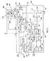
- FIG. 3 is a detailed block diagram of the device of FIG. 1 ;
- FIG. 4 illustrates input waveforms to the device of FIG. 1 ;
- FIGS. 5 and 6 illustrates detailed waveforms
- FIG. 7 is a waveform of the voltage across one of the motor windings before adding the improvement of the invention.
- FIGS. 8 and 10 illustrate the voltages applied to the motor windings in accordance with the principles of the invention.
- FIG. 9 illustrates a portion of the block diagram of FIG. 3 in greater detail.
- the illustrative embodiment of the invention is a monolithic brushless DC motor controller 100 that provides functions for implementing fan speed control. As shown in FIG. 1 , the invention may be implemented in one configuration as an eight pin package.
- Controller 100 may be provided in SOP-8 and MSOP-8 surface mount packages. In other embodiments of the invention controller 100 may be integrated onto the same silicon as the device being cooled by fan 200 .
- controller 100 for speed control of motor 200 includes a pulse width modulator logic or PWM circuit 101 , commutation logic for proper drive sequencing 103 , direct motor drive 105 , current limiter 107 , and a programmable fault timer with time delayed restart and a power down low current mode block 109 .
- Controller 100 fully integrated on a single chip 102 contains all required functions for implementing fan speed control.
- pulse width modulator (PWM) 101 comprising a fixed frequency oscillator 301 , comparator 303 , and a latch 305 along with associated gates for motor speed control of motor 200 .
- Controller 100 also includes commutation logic 103 for proper drive sequencing, on-chip power MOSFETs 313 , 315 for direct motor drive, cycle-by-cycle current limiting circuit 317 , and a circuit block 319 providing a programmable fault timer with time delayed restart, and a power down low current mode.
- Motor 200 includes rotor 201 and stator windings 203 , 205 .
- a rotator position sensor 207 is provided with motor 200 .
- a Hall effect device sensor is utilized is utilized as sensor 207 .
- Motor 200 includes connections ⁇ 1 , ⁇ 2 , a sensor output HALL and power connections.
- Controller 100 utilizes pulse width modulation to provide an energy efficient means for controlling the motor speed of fan motor 200 by varying the average applied voltage to each stator winding 203 , 205 during the commutation sequence.
- PWM circuit 101 as noted above includes oscillator 301 , comparator 303 , and latch 305 . Oscillator 301 provides both pulse and saw tooth outputs. PWM circuit 101 is responsive to either an analog or a digital signal on the same input terminal PWM Input.
- FIG. 4 illustrates the analog input signal range 401 and a digital input signal range 405 that PWM logic 101 is responsive to in the illustrative embodiment are shown.
- PWM circuit 101 includes a sub-circuit comprising level comparators 331 , 333 and a NOR gate 348 that is used to determine whether the control signal at terminal PWM Input is a digital control signal. If the control signal is not digital, it is assumed to be analog.
- Comparator 331 has an input coupled to terminal PWM Input and compares the voltage at PWM Input against a reference that corresponds to the minimum logic high level.
- the minimum logic high voltage level is 2.5 volts. Comparator 331 generates a logic 1 or high output if the voltage at PWM Input exceeds 2.5 volts.
- Comparator 333 has an input coupled to terminal PWM Input and compares the voltage at PWM Input against a reference that corresponds to the maximum logic low level.
- the maximum logic low voltage level is 0.5 volts. Comparator 333 generates a logic 1 or high output if the voltage at PWM Input is less than 0.5 volts.
- Nor gate 348 provides a logic 0 or low output if either comparator 331 or comparator 333 indicates that the control signal is digital and provides a logic 1 or high output if neither comparator 331 or 333 indicates that the control signal is a digital signal.
- gates 341 - 348 Operation of gates 341 - 348 is as follows: AND gate 341 has one input coupled to the square wave output of oscillator 301 and its other input coupled to the output of gate 348 . Gate 341 blocks pulses from Oscillator 301 if a digital signal is present at PWM Input. This prevents Oscillator 301 from initiating operation of Motor Drive circuit 316 via latch 305 when a digital signal is present at PWM Input.
- AND gate 342 has one input coupled to the output of PWM comparator 303 and its other input coupled to the output of gate 348 .
- Gate 342 blocks the PWM comparator output pulses if a digital signal is present at PWM Input. This prevents PWM comparator 303 from terminating operation of Motor Drive circuit 316 via latch 305 when a digital signal is present at PWM Input.
- Gate 343 is used to block signals to latch 305 reset input R during the time that current limiter 317 detects that the motor current exceeds a predetermined limit. This prevents PWM comparator 303 from initiating energization of motor drive circuit 316 .
- Gate 344 allows the pulse output from Oscillator 301 to reset latch 305 if there is no current limiting and no analog input control signal comparison from comparator 303 .
- Gate 347 is used to terminate energization of motor drive circuit 316 from either a digital low PWM INPUT signal, or a comparison from comparator 303 , or the current limiter circuit 317 detects that the drive current limit is exceeded.
- Gate 346 is utilized to reset latch 305 to initiate on-time of motor drive circuit 316 .
- Gate 347 sets latch 305 to terminate the on-time of motor drive circuit 316 .
- Waveform 501 is the saw tooth output waveform of Oscillator 301 .
- Waveform 503 is the Analog signal control at PWM Input.
- Waveform 505 is the output of current limit circuit 317 .
- Waveform 507 is the reset input R of PWM latch 305 .
- Waveform 509 is the output Q′ of PWM latch 305 .
- Analog signal input control is accomplished with Oscillator 301 initiating Motor Drive conduction and the PWM Comparator 303 terminating it.
- a pulse 511 is simultaneously generated at the oscillator output 507 to reset PWM Latch 305 , thereby causing the output Q′ to attain a high level allowing conduction of a Motor Drive MOSFET 313 , 315 .
- PWM Comparator 303 terminates conduction when saw tooth waveform 501 rises above the voltage level of the analog control waveform 503 applied to PWM Input.
- the conduction duty cycle or average voltage applied to a stator winding 203 , 205 of fan motor 200 is directly controlled by the analog voltage at PWM Input.
- the conduction duty cycle increases from 0% to 100% as illustrated by waveform 509 as PWM Input voltage increases from 1.0 V to 2.0 V, respectively.
- Waveform 603 is a representative waveform of an input digital signal control at PWM Input.
- Waveform 505 is the output of current limit comparator 317 .
- Waveform 507 is the reset input R of PWM latch 305 .
- Waveform 509 is the output Q′ of PWM latch 305 .
- Digital control is accomplished by applying a digital signal of the desired conduction duty cycle to the PWM Input.
- the low VIL and high VIH states for the digital input encompass the internal saw tooth peak and valley levels.
- saw tooth levels are chosen such that a maximum 0.5 V low state and a minimum 2.5 V high state digital signal are utilized. These levels are easily achievable by 3.0 V logic circuitry.
- Latch 305 when reset, initiates conduction of a Motor Drive MOSFET 313 , 315 .
- Latch 305 when set, terminates conduction of Motor Drive MOSFETs 313 , 315 .
- the conduction duty cycle is directly controlled by the signal duty cycle present at the PWM Input as long as the signal magnitude is above and below the window detector thresholds provided by comparators 331 , 333 .
- Commutation logic 103 includes a rotor position decoder coupled to HALL input to monitor which in turn is connectable to Hall sensor 207 .
- Rotor position decoder provides proper sequencing of the Phase 1, ⁇ 1, and Phase 2, ⁇ 2 drive outputs.
- Hall input is designed to interface directly with an open collector type Hall Effect switch.
- An internal pull-up is provided to minimize to number of external components.
- the Commutation Logic provides an output signal for monitoring the motor speed at output Tach.
- Direct motor drive is accomplished by providing two on-chip open drain N-channel MOSFETs 313 , 315 , each having a high breakdown voltage.
- the respective MOSFET 313 , 315 drains are pinned out to output terminals ⁇ 1 , ⁇ 2 for direct connection to motor windings 203 , 205 .
- Zener and series diodes 314 , 314 a are connected from each respective MOSFET drain to gate to protect the MOSFETs 313 , 315 from excessive inductive voltage spikes.
- Current limit comparator 317 monitors the voltage drop that appears across a sense resistor 318 . If motor 201 becomes overloaded or stalls, the threshold level of current limit circuit 317 will be exceeded causing PWM Latch 305 to set. This terminates conduction of the Motor Drive MOSFETs 313 , 315 on an oscillator cycle-by-cycle basis.
- the Fault Timer 109 is controlled by the value of the external capacitor 110 .
- a current source included in fault timer 109 is used to charge capacitor 110 .
- the Fault Time mode is initiated when the current limit circuit 317 is activated. If an over current situation persists for an extended time period, the Fault Timer will gradually discharge the external timing capacitor to a voltage level that will cause the motor to stop and then initiate a restart sequence.
- a power control circuit 369 is connected to the PWM input terminal. Power control circuit 369 monitors the signal level at PWM input. If the signal level at PWM input is below the minimum signal level for both digital and analog control signals for a predetermined time, power control circuit 369 signals circuit 109 to enter the power down or “sleep” mode wherein, power drain is reduced. This advantageously eliminates the need to provide separate power down control signals. Operation of the power control circuit is automatic. Power control circuit thus automatically reduces in device drain current at zero fan speed after time out.
- power control circuit 369 automatically powers down control circuit 100 if the system is at zero fan speed for a predetermined time.
- the fan is stopped and a timer in power control circuit 369 initiates a time period. If the signal level at PWM input rises to one volt or above, then the timer is turned off. The timer is set so that the predetermined time period selected is greater than the time period between pulses of the digital control signal. In the embodiment shown, a time period of two seconds is utilized as the predetermined period of time. However, those skilled in the art will understand that other time periods may be utilized.
- control circuit 100 is fully powered up.
- power control circuit 369 Although those skilled in the art are aware that many circuit configurations can be provided for power control circuit 369 .
- a level comparator 371 and a timer 373 are utilized to provide the power control function.
- Motor winding leakage inductance is due to the relatively poor or low mutual coupling between the phase 1 and phase 2 windings 205 , 203 .
- a high voltage turn-off spike is generated by the energy that was stored in the leakage inductance during the on-time. This energy must be absorbed to prevent destruction of the motor drive MOSFETs 315 , 314 . This is usually accomplished with the addition of a capacitive snubber circuit 387 . Capacitive snubbing will extend the turn-off voltage rise time.
- FIG. 7 illustrates this problem that occurs in prior art motor controllers. Because of the low mutual coupling that exists between the motor windings 203 , 205 , a significant leakage inductance spike will typically occur each time one of the windings is de-energized. This problem manifests itself in a spike at the leading edge of the pulsed motor winding and may exceed twice the magnitude of the supply voltage V DD that is applied to the motor windings 203 , 205 .
- phase 2 winding 203 early tends to reduce the leakage inductance voltage spike but at the expense of creating a current spike in the motor power source V DD .
- the energization of each winding 203 , 205 is delayed by a time t as shown in FIG. 8 so that the leakage inductance voltage is significantly less than the applied voltage V DD .
- the delay time t is in the range of 10 to 200 microseconds.
- the delay time t is proportional to the inductance of windings 203 , 205 .
- the optimum time to turn-on phase 2 winding 203 is after the current has decayed in phase 1 winding 205 .
- This time is variable depending upon the motor leakage inductance, winding mutual coupling, and snubber capacitance 387 used.
- the optimum time to turn-on phase 2 winding 203 is determined by monitoring the voltage on phase 1 winding 205 .
- the current spike induced in V DD is reduced significantly, thus reducing EMI and RFI.
- the commutation delay becomes automatically adaptive to the motor characteristics and the snubber circuit 387 .
- Voltage threshold circuits 383 and 385 are coupled across motor windings 205 , 203 , respectively.
- Voltage threshold circuits 383 , 385 each monitor the voltage across the respective winding and each provides an output that is coupled to delay circuit 387 that controls commutation circuit 103 such that the turn on falling edge of each pulse applied to one winding is delayed by the time t that occurs after the turn off rising edge of the pulse applied to the other winding.
- the adaptive non-overlapping commutation delay circuit 381 prevents simultaneous drive conduction for reduced power supply current spikes and radio frequency interference (RFI).
- the non-overlap time t is internally set to a minimum of 20 ⁇ s.
- Circuit 381 monitors the rise in turn-off voltage at each drive output ⁇ 1 , ⁇ 2 and dynamically extends time t. The voltage level at the initially turned off output must reach V DD before turn on of the next output is allowed.
- FIG. 10 commutation waveforms are shown for the instance where there is a minimum or overlapping time t 1 and for the instance where there is a delay time t.
- the adaptive delay time t is automatic and insures non-overlapping commutation even when large value snubber capacitors 387 are used.
- Adaptive non-overlapping commutation delay circuit 381 prevents simultaneous drive conduction as shown in the waveforms on the left side of FIG. 10 which produce power supply current spikes and resulting radio frequency interference (RFI).
- Circuit 381 provides for a preset minimum non-overlap time of 20 ⁇ s.
- Circuit 381 operates to dynamically extend the non-overlap time by monitoring the rise in turn-off voltage at each drive output. The voltage level at the initially turned off output must reach V DD before turn on of the next output is allowed.
- the adaptive delay time t is automatic and insures non-overlapping commutation even when large value snubber capacitors 387 are used.
- circuit 381 is formed on the same integrated circuit 100 that the rest of the controller circuit is formed on.
- Controller 100 advantageously provides the following and other features:
- Controller 100 has many applications, including:
Abstract
Description
-
- Interfaces directly with aSC7611 thermal controller;
- Analog and digital PWM control signal compatibility;
- Motor fault timeout with auto start retry;
- Fan tachometer output for closed loop speed control;
- Latching PWM for enhanced noise immunity;
- Cycle-by-cycle current limit protection;
- On-
chip 1 Ohm motor drivers; - Automatically initiated Low current power down mode;
- Minimum number of external components; and
- 8-lead SOIC or MSOP package
-
- Personal and notebook computers fans;
- Workstation and mainframe fans;
- LAN server blowers;
- Industrial control system fans;
- Telcom system fans;
- Instrumentation test and measurement fans; and
- Card rack fans.
Claims (19)
Priority Applications (1)
| Application Number | Priority Date | Filing Date | Title |
|---|---|---|---|
| US11/080,344 US7276867B2 (en) | 2004-11-10 | 2005-03-15 | Controller arrangement with adaptive non-overlapping commutation |
Applications Claiming Priority (2)
| Application Number | Priority Date | Filing Date | Title |
|---|---|---|---|
| US10/985,754 US7030584B1 (en) | 2004-09-27 | 2004-11-10 | Controller arrangement |
| US11/080,344 US7276867B2 (en) | 2004-11-10 | 2005-03-15 | Controller arrangement with adaptive non-overlapping commutation |
Related Parent Applications (1)
| Application Number | Title | Priority Date | Filing Date |
|---|---|---|---|
| US10/985,754 Continuation-In-Part US7030584B1 (en) | 2004-09-27 | 2004-11-10 | Controller arrangement |
Publications (2)
| Publication Number | Publication Date |
|---|---|
| US20060097678A1 US20060097678A1 (en) | 2006-05-11 |
| US7276867B2 true US7276867B2 (en) | 2007-10-02 |
Family
ID=46321849
Family Applications (1)
| Application Number | Title | Priority Date | Filing Date |
|---|---|---|---|
| US11/080,344 Active 2025-11-10 US7276867B2 (en) | 2004-11-10 | 2005-03-15 | Controller arrangement with adaptive non-overlapping commutation |
Country Status (1)
| Country | Link |
|---|---|
| US (1) | US7276867B2 (en) |
Cited By (18)
| Publication number | Priority date | Publication date | Assignee | Title |
|---|---|---|---|---|
| US20080030154A1 (en) * | 2006-08-04 | 2008-02-07 | Foxconn Technology Co., Ltd. | Apparatuses and methods for controlling rotational direction of fan |
| US20080245237A1 (en) * | 2003-12-30 | 2008-10-09 | Haverstock Thomas B | Coffee infusion press for stackable cups |
| US20080253750A1 (en) * | 2007-03-13 | 2008-10-16 | Jao-Ching Lin | Protect-control device capable of limiting current for reducing noise resultling from switchover of motor |
| US20080273865A1 (en) * | 2007-05-01 | 2008-11-06 | Andigilog, Inc. | Noise suppresion suppression for hall sensor arrangements |
| US20090039820A1 (en) * | 2007-08-08 | 2009-02-12 | Milano Shaun D | Motor controller having a multifunction port |
| US20090039807A1 (en) * | 2007-08-08 | 2009-02-12 | Hitoshi Yabusaki | Motor controller |
| US20090066280A1 (en) * | 2006-01-23 | 2009-03-12 | Rohm Co., Ltd. | Motor drive circuit and cooling system using same |
| US20100231147A1 (en) * | 2009-03-12 | 2010-09-16 | Milesi Alejandro G | Braking function for brushless dc motor control |
| US20110181211A1 (en) * | 2010-01-28 | 2011-07-28 | Sanyo Electric Co., Ltd. | Drive control circuit for linear vibration motor |
| US20110204834A1 (en) * | 2010-02-23 | 2011-08-25 | On Semiconductor Trading, Ltd. | Motor driving circuit |
| US20110298398A1 (en) * | 2010-06-04 | 2011-12-08 | Sanyo Denki Co., Ltd. | Driving system for fan and method of driving fan |
| US20130062138A1 (en) * | 2011-09-08 | 2013-03-14 | Denso Corporation | Rotating electrical machine control device and steering control system |
| US8421434B2 (en) | 2006-06-02 | 2013-04-16 | Dolpan Audio, Llc | Bandgap circuit with temperature correction |
| US20140042952A1 (en) * | 2012-08-09 | 2014-02-13 | Samsung Electro-Mechanics Co., Ltd. | Apparatus and method for preventing sensing error in srm |
| US8736202B2 (en) | 2010-05-13 | 2014-05-27 | Semiconductor Components Industries, Llc | Drive control circuit for linear vibration motor |
| US8736201B2 (en) | 2010-05-13 | 2014-05-27 | Semiconductor Components Industries, Llc | Drive control circuit for linear vibration motor |
| US9877629B2 (en) | 2013-02-08 | 2018-01-30 | Techtronic Industries Co. Ltd. | Battery-powered cordless cleaning system |
| US10326391B2 (en) * | 2017-03-30 | 2019-06-18 | Melexis Bulgaria Ltd. | Motordriver for PWM driven motors |
Families Citing this family (4)
| Publication number | Priority date | Publication date | Assignee | Title |
|---|---|---|---|---|
| US7233121B2 (en) * | 2003-07-04 | 2007-06-19 | Delta Electronics, Inc. | Fan speed control circuit |
| TWI226148B (en) * | 2003-07-04 | 2005-01-01 | Delta Electronics Inc | Phase and pulse width modulation fan speed control circuit |
| JP2006204063A (en) * | 2005-01-24 | 2006-08-03 | Denso Corp | Method and apparatus for controlling semiconductor device |
| US7778324B2 (en) * | 2005-11-18 | 2010-08-17 | Harman International Industries, Incorporated | System for dynamic time offsetting in interleaved power amplifiers |
Citations (5)
| Publication number | Priority date | Publication date | Assignee | Title |
|---|---|---|---|---|
| US4434389A (en) * | 1980-10-28 | 1984-02-28 | Kollmorgen Technologies Corporation | Motor with redundant windings |
| US4859921A (en) * | 1988-03-10 | 1989-08-22 | General Electric Company | Electronic control circuits, electronically commutated motor systems, switching regulator power supplies, and methods |
| US5306988A (en) * | 1991-10-03 | 1994-04-26 | Sgs-Thomson Microelectronics, Inc. | Method and apparatus for operating polyphase dc motors |
| US5668449A (en) * | 1994-10-27 | 1997-09-16 | Sgs-Thomson Microelectronics, Inc. | Motor with input-controlled high side driver |
| US6661190B1 (en) * | 2002-05-23 | 2003-12-09 | The Boeing Company | Controller and associated drive assembly controlling a brushless direct current motor |
-
2005
- 2005-03-15 US US11/080,344 patent/US7276867B2/en active Active
Patent Citations (5)
| Publication number | Priority date | Publication date | Assignee | Title |
|---|---|---|---|---|
| US4434389A (en) * | 1980-10-28 | 1984-02-28 | Kollmorgen Technologies Corporation | Motor with redundant windings |
| US4859921A (en) * | 1988-03-10 | 1989-08-22 | General Electric Company | Electronic control circuits, electronically commutated motor systems, switching regulator power supplies, and methods |
| US5306988A (en) * | 1991-10-03 | 1994-04-26 | Sgs-Thomson Microelectronics, Inc. | Method and apparatus for operating polyphase dc motors |
| US5668449A (en) * | 1994-10-27 | 1997-09-16 | Sgs-Thomson Microelectronics, Inc. | Motor with input-controlled high side driver |
| US6661190B1 (en) * | 2002-05-23 | 2003-12-09 | The Boeing Company | Controller and associated drive assembly controlling a brushless direct current motor |
Cited By (34)
| Publication number | Priority date | Publication date | Assignee | Title |
|---|---|---|---|---|
| US20080245237A1 (en) * | 2003-12-30 | 2008-10-09 | Haverstock Thomas B | Coffee infusion press for stackable cups |
| US8084973B2 (en) * | 2006-01-23 | 2011-12-27 | Rohm Co., Ltd. | Motor driving circuit |
| US20090066280A1 (en) * | 2006-01-23 | 2009-03-12 | Rohm Co., Ltd. | Motor drive circuit and cooling system using same |
| US8421434B2 (en) | 2006-06-02 | 2013-04-16 | Dolpan Audio, Llc | Bandgap circuit with temperature correction |
| US8941370B2 (en) | 2006-06-02 | 2015-01-27 | Doplan Audio, LLC | Bandgap circuit with temperature correction |
| US9671800B2 (en) | 2006-06-02 | 2017-06-06 | Ol Security Limited Liability Company | Bandgap circuit with temperature correction |
| US20080030154A1 (en) * | 2006-08-04 | 2008-02-07 | Foxconn Technology Co., Ltd. | Apparatuses and methods for controlling rotational direction of fan |
| US7492112B2 (en) * | 2006-08-04 | 2009-02-17 | Fu Zhun Precision Industry (Shen Zhen) Co., Ltd. | Apparatuses and methods for controlling rotational direction of fan |
| US20080253750A1 (en) * | 2007-03-13 | 2008-10-16 | Jao-Ching Lin | Protect-control device capable of limiting current for reducing noise resultling from switchover of motor |
| US7518330B2 (en) * | 2007-03-13 | 2009-04-14 | Sentelic Corporation | Protect-control device capable of limiting current for reducing noise resultling from switchover of motor |
| US20080273865A1 (en) * | 2007-05-01 | 2008-11-06 | Andigilog, Inc. | Noise suppresion suppression for hall sensor arrangements |
| US20090230904A1 (en) * | 2007-05-01 | 2009-09-17 | Alberkrack Jade H | Noise suppression for hall sensor arrangements |
| US7705550B2 (en) | 2007-05-01 | 2010-04-27 | Alberkrack Jade H | Noise suppression for hall sensor arrangements |
| US7538505B2 (en) * | 2007-05-01 | 2009-05-26 | Alberkrack Jade H | Noise suppresion suppression for hall sensor arrangements |
| US7590334B2 (en) * | 2007-08-08 | 2009-09-15 | Allegro Microsystems, Inc. | Motor controller |
| US7747146B2 (en) | 2007-08-08 | 2010-06-29 | Allegro Microsystems, Inc. | Motor controller having a multifunction port |
| US20090039807A1 (en) * | 2007-08-08 | 2009-02-12 | Hitoshi Yabusaki | Motor controller |
| US20090039820A1 (en) * | 2007-08-08 | 2009-02-12 | Milano Shaun D | Motor controller having a multifunction port |
| US20100231147A1 (en) * | 2009-03-12 | 2010-09-16 | Milesi Alejandro G | Braking function for brushless dc motor control |
| US8093844B2 (en) | 2009-03-12 | 2012-01-10 | Allegro Microsystems, Inc. | Braking function for brushless DC motor control |
| US20110181211A1 (en) * | 2010-01-28 | 2011-07-28 | Sanyo Electric Co., Ltd. | Drive control circuit for linear vibration motor |
| US8519645B2 (en) * | 2010-01-28 | 2013-08-27 | Semiconductor Components Industries, Llc | Drive control circuit for linear vibration motor |
| TWI455477B (en) * | 2010-01-28 | 2014-10-01 | Sanyo Electric Co | Driving control circuit for linear vibration motor |
| US20110204834A1 (en) * | 2010-02-23 | 2011-08-25 | On Semiconductor Trading, Ltd. | Motor driving circuit |
| US8368332B2 (en) * | 2010-02-23 | 2013-02-05 | On Semiconductor Trading, Ltd. | Motor driving circuit |
| US8736202B2 (en) | 2010-05-13 | 2014-05-27 | Semiconductor Components Industries, Llc | Drive control circuit for linear vibration motor |
| US8736201B2 (en) | 2010-05-13 | 2014-05-27 | Semiconductor Components Industries, Llc | Drive control circuit for linear vibration motor |
| US8680800B2 (en) * | 2010-06-04 | 2014-03-25 | Sanyo Denki Co., Ltd. | Driving system for fan and method of driving fan |
| US20110298398A1 (en) * | 2010-06-04 | 2011-12-08 | Sanyo Denki Co., Ltd. | Driving system for fan and method of driving fan |
| US8813905B2 (en) * | 2011-09-08 | 2014-08-26 | Denso Corporation | Rotating electrical machine control device and steering control system |
| US20130062138A1 (en) * | 2011-09-08 | 2013-03-14 | Denso Corporation | Rotating electrical machine control device and steering control system |
| US20140042952A1 (en) * | 2012-08-09 | 2014-02-13 | Samsung Electro-Mechanics Co., Ltd. | Apparatus and method for preventing sensing error in srm |
| US9877629B2 (en) | 2013-02-08 | 2018-01-30 | Techtronic Industries Co. Ltd. | Battery-powered cordless cleaning system |
| US10326391B2 (en) * | 2017-03-30 | 2019-06-18 | Melexis Bulgaria Ltd. | Motordriver for PWM driven motors |
Also Published As
| Publication number | Publication date |
|---|---|
| US20060097678A1 (en) | 2006-05-11 |
Similar Documents
| Publication | Publication Date | Title |
|---|---|---|
| US7276867B2 (en) | Controller arrangement with adaptive non-overlapping commutation | |
| US7064510B2 (en) | Controller arrangement with automatic power down | |
| US5483141A (en) | Method and apparatus for controlling refrigerator cycle | |
| US6528968B2 (en) | Brushless-motor driver in PWM mode | |
| US8084973B2 (en) | Motor driving circuit | |
| US9143079B2 (en) | Power converter | |
| JP4076376B2 (en) | Drive device | |
| US7315439B2 (en) | Method and circuit arrangement for limiting an overvoltage | |
| US4958121A (en) | Protection of power converters from voltage spikes | |
| US7622873B2 (en) | Motor drive device and drive method | |
| US7030584B1 (en) | Controller arrangement | |
| US9985560B2 (en) | Motor controller and method for controlling motor | |
| JP2004282920A (en) | Motor controller | |
| US8503146B1 (en) | Gate driver with short-circuit protection | |
| US20160079904A1 (en) | Drive unit employing gallium nitride switches | |
| JP2000333441A (en) | Gate control circuit for insulated gate semiconductor device | |
| EP3975402A1 (en) | A discharge control circuit, corresponding system, vehicle and method | |
| US20060208821A1 (en) | Controller arrangement | |
| US10218295B2 (en) | Motor drive controller and method for controlling motor | |
| JP6374891B2 (en) | Motor drive control device and motor drive control method thereof | |
| US11770081B2 (en) | Braking of single coil BLDC motors | |
| US11784487B2 (en) | Overvoltage protecting system and method of motor pre-driver | |
| EP2034322B1 (en) | Control circuit for driving a semiconductor switch | |
| JP7249740B2 (en) | MOTOR DRIVE DEVICE, MOTOR SYSTEM, FAN MOTOR AND MOTOR DRIVING METHOD | |
| US10879887B2 (en) | Smart turn-off for gate driver circuit |
Legal Events
| Date | Code | Title | Description |
|---|---|---|---|
| AS | Assignment |
Owner name: PALISADES NON-QUALIFIED INVESTORS, L.P., CALIFORNI Free format text: SECURITY AGREEMENT;ASSIGNOR:ANDIGILOG, INC.;REEL/FRAME:016153/0080 Effective date: 20050616 Owner name: MISSION VENTURES AFFILIATES II, L.P., CALIFORNIA Free format text: SECURITY AGREEMENT;ASSIGNOR:ANDIGILOG, INC.;REEL/FRAME:016153/0080 Effective date: 20050616 Owner name: VALLEY VENTURES III, L.P., ARIZONA Free format text: SECURITY AGREEMENT;ASSIGNOR:ANDIGILOG, INC.;REEL/FRAME:016153/0080 Effective date: 20050616 Owner name: PALISADES QUALIFIED INVESTORS, L.P., CALIFORNIA Free format text: SECURITY AGREEMENT;ASSIGNOR:ANDIGILOG, INC.;REEL/FRAME:016153/0080 Effective date: 20050616 Owner name: MISSION VENTURES II, L.P., CALIFORNIA Free format text: SECURITY AGREEMENT;ASSIGNOR:ANDIGILOG, INC.;REEL/FRAME:016153/0080 Effective date: 20050616 Owner name: PALISADES VENTURES, L.P., CALIFORNIA Free format text: SECURITY AGREEMENT;ASSIGNOR:ANDIGILOG, INC.;REEL/FRAME:016153/0080 Effective date: 20050616 |
|
| AS | Assignment |
Owner name: ANDIGILOG, INC., ARIZONA Free format text: ASSIGNMENT OF ASSIGNORS INTEREST;ASSIGNORS:BRANNEN, ROBERT ALAN;ALBERKRACK, JADE H.;REEL/FRAME:017013/0951 Effective date: 20050228 |
|
| AS | Assignment |
Owner name: VENTURE LENDING & LEASING IV, INC., CALIFORNIA Free format text: SECURITY AGREEMENT;ASSIGNOR:ANDIGILOG, INC.;REEL/FRAME:017065/0592 Effective date: 20050919 |
|
| AS | Assignment |
Owner name: ANDIGILOG, INC., ARIZONA Free format text: RELEASE BY SECURED PARTY;ASSIGNORS:VALLEY VENTURES III, L.P.;MISSION VENTURES II, L.P.;MISSION VENTURES AFFILIATES II, L.P.;AND OTHERS;REEL/FRAME:017230/0862 Effective date: 20060223 |
|
| AS | Assignment |
Owner name: VALLEY VENTURES III, L.P.,ARIZONA Free format text: SECURITY AGREEMENT;ASSIGNOR:ANDIGILOG, INC.;REEL/FRAME:017996/0519 Effective date: 20060725 Owner name: MISSION VENTURES II, L.P.,CALIFORNIA Free format text: SECURITY AGREEMENT;ASSIGNOR:ANDIGILOG, INC.;REEL/FRAME:017996/0519 Effective date: 20060725 Owner name: MISSION VENTURES AFFILIATES II, L.P.,CALIFORNIA Free format text: SECURITY AGREEMENT;ASSIGNOR:ANDIGILOG, INC.;REEL/FRAME:017996/0519 Effective date: 20060725 Owner name: PALISADES VENTURES, L.P.,CALIFORNIA Free format text: SECURITY AGREEMENT;ASSIGNOR:ANDIGILOG, INC.;REEL/FRAME:017996/0519 Effective date: 20060725 Owner name: PALISADES QUALIFIED INVESTORS, L.P.,CALIFORNIA Free format text: SECURITY AGREEMENT;ASSIGNOR:ANDIGILOG, INC.;REEL/FRAME:017996/0519 Effective date: 20060725 Owner name: PALISADES NON-QUALIFIED INVESTORS, L.P.,CALIFORNIA Free format text: SECURITY AGREEMENT;ASSIGNOR:ANDIGILOG, INC.;REEL/FRAME:017996/0519 Effective date: 20060725 Owner name: OM ANDIGILOG INVESTORS II, LLC,ARIZONA Free format text: SECURITY AGREEMENT;ASSIGNOR:ANDIGILOG, INC.;REEL/FRAME:017996/0519 Effective date: 20060725 Owner name: VALLEY VENTURES III, L.P., ARIZONA Free format text: SECURITY AGREEMENT;ASSIGNOR:ANDIGILOG, INC.;REEL/FRAME:017996/0519 Effective date: 20060725 Owner name: MISSION VENTURES AFFILIATES II, L.P., CALIFORNIA Free format text: SECURITY AGREEMENT;ASSIGNOR:ANDIGILOG, INC.;REEL/FRAME:017996/0519 Effective date: 20060725 Owner name: OM ANDIGILOG INVESTORS II, LLC, ARIZONA Free format text: SECURITY AGREEMENT;ASSIGNOR:ANDIGILOG, INC.;REEL/FRAME:017996/0519 Effective date: 20060725 Owner name: PALISADES VENTURES, L.P., CALIFORNIA Free format text: SECURITY AGREEMENT;ASSIGNOR:ANDIGILOG, INC.;REEL/FRAME:017996/0519 Effective date: 20060725 Owner name: PALISADES QUALIFIED INVESTORS, L.P., CALIFORNIA Free format text: SECURITY AGREEMENT;ASSIGNOR:ANDIGILOG, INC.;REEL/FRAME:017996/0519 Effective date: 20060725 Owner name: MISSION VENTURES II, L.P., CALIFORNIA Free format text: SECURITY AGREEMENT;ASSIGNOR:ANDIGILOG, INC.;REEL/FRAME:017996/0519 Effective date: 20060725 Owner name: PALISADES NON-QUALIFIED INVESTORS, L.P., CALIFORNI Free format text: SECURITY AGREEMENT;ASSIGNOR:ANDIGILOG, INC.;REEL/FRAME:017996/0519 Effective date: 20060725 |
|
| AS | Assignment |
Owner name: VALLEY VENTURES III, L.P.,ARIZONA Free format text: SECURITY AGREEMENT;ASSIGNOR:ANDIGILOG, INC.;REEL/FRAME:018490/0055 Effective date: 20061031 Owner name: MISSION VENTURES II, L.P.,CALIFORNIA Free format text: SECURITY AGREEMENT;ASSIGNOR:ANDIGILOG, INC.;REEL/FRAME:018490/0055 Effective date: 20061031 Owner name: MISSION VENTURES AFFILIATES II, L.P.,CALIFORNIA Free format text: SECURITY AGREEMENT;ASSIGNOR:ANDIGILOG, INC.;REEL/FRAME:018490/0055 Effective date: 20061031 Owner name: PALISADES VENTURES, L.P.,CALIFORNIA Free format text: SECURITY AGREEMENT;ASSIGNOR:ANDIGILOG, INC.;REEL/FRAME:018490/0055 Effective date: 20061031 Owner name: PALISADES QUALIFIED INVESTORS, L.P.,CALIFORNIA Free format text: SECURITY AGREEMENT;ASSIGNOR:ANDIGILOG, INC.;REEL/FRAME:018490/0055 Effective date: 20061031 Owner name: PALISADES NON-QUALIFIED INVESTORS, L.P.,CALIFORNIA Free format text: SECURITY AGREEMENT;ASSIGNOR:ANDIGILOG, INC.;REEL/FRAME:018490/0055 Effective date: 20061031 Owner name: OM ANDIGILOG INVESTORS II, LLC,ARIZONA Free format text: SECURITY AGREEMENT;ASSIGNOR:ANDIGILOG, INC.;REEL/FRAME:018490/0055 Effective date: 20061031 Owner name: VENTURE LENDING & LEASING IV, LLC,CALIFORNIA Free format text: SECURITY AGREEMENT;ASSIGNOR:ANDIGILOG, INC.;REEL/FRAME:018490/0055 Effective date: 20061031 Owner name: LIEPOLD, CARL F,ARIZONA Free format text: SECURITY AGREEMENT;ASSIGNOR:ANDIGILOG, INC.;REEL/FRAME:018490/0055 Effective date: 20061031 Owner name: LIEPOLD, CARL F, ARIZONA Free format text: SECURITY AGREEMENT;ASSIGNOR:ANDIGILOG, INC.;REEL/FRAME:018490/0055 Effective date: 20061031 Owner name: PALISADES QUALIFIED INVESTORS, L.P., CALIFORNIA Free format text: SECURITY AGREEMENT;ASSIGNOR:ANDIGILOG, INC.;REEL/FRAME:018490/0055 Effective date: 20061031 Owner name: MISSION VENTURES AFFILIATES II, L.P., CALIFORNIA Free format text: SECURITY AGREEMENT;ASSIGNOR:ANDIGILOG, INC.;REEL/FRAME:018490/0055 Effective date: 20061031 Owner name: VALLEY VENTURES III, L.P., ARIZONA Free format text: SECURITY AGREEMENT;ASSIGNOR:ANDIGILOG, INC.;REEL/FRAME:018490/0055 Effective date: 20061031 Owner name: PALISADES NON-QUALIFIED INVESTORS, L.P., CALIFORNI Free format text: SECURITY AGREEMENT;ASSIGNOR:ANDIGILOG, INC.;REEL/FRAME:018490/0055 Effective date: 20061031 Owner name: PALISADES VENTURES, L.P., CALIFORNIA Free format text: SECURITY AGREEMENT;ASSIGNOR:ANDIGILOG, INC.;REEL/FRAME:018490/0055 Effective date: 20061031 Owner name: MISSION VENTURES II, L.P., CALIFORNIA Free format text: SECURITY AGREEMENT;ASSIGNOR:ANDIGILOG, INC.;REEL/FRAME:018490/0055 Effective date: 20061031 Owner name: OM ANDIGILOG INVESTORS II, LLC, ARIZONA Free format text: SECURITY AGREEMENT;ASSIGNOR:ANDIGILOG, INC.;REEL/FRAME:018490/0055 Effective date: 20061031 Owner name: VENTURE LENDING & LEASING IV, LLC, CALIFORNIA Free format text: SECURITY AGREEMENT;ASSIGNOR:ANDIGILOG, INC.;REEL/FRAME:018490/0055 Effective date: 20061031 |
|
| STCF | Information on status: patent grant |
Free format text: PATENTED CASE |
|
| FEPP | Fee payment procedure |
Free format text: PAYOR NUMBER ASSIGNED (ORIGINAL EVENT CODE: ASPN); ENTITY STATUS OF PATENT OWNER: LARGE ENTITY |
|
| AS | Assignment |
Owner name: VALLEY VENTURES III, L.P., ARIZONA Free format text: SECURITY AGREEMENT;ASSIGNOR:ANDIGILOG, INC.;REEL/FRAME:020645/0218 Effective date: 20080304 Owner name: VALLEY VENTURES III ANNEX, L.P., ARIZONA Free format text: SECURITY AGREEMENT;ASSIGNOR:ANDIGILOG, INC.;REEL/FRAME:020645/0218 Effective date: 20080304 Owner name: MISSION VENTURES II, L.P., CALIFORNIA Free format text: SECURITY AGREEMENT;ASSIGNOR:ANDIGILOG, INC.;REEL/FRAME:020645/0218 Effective date: 20080304 Owner name: MISSION VENTURES AFFILIATES II, L.P., CALIFORNIA Free format text: SECURITY AGREEMENT;ASSIGNOR:ANDIGILOG, INC.;REEL/FRAME:020645/0218 Effective date: 20080304 Owner name: INLIGN CP IV, LLC, ARIZONA Free format text: SECURITY AGREEMENT;ASSIGNOR:ANDIGILOG, INC.;REEL/FRAME:020645/0218 Effective date: 20080304 Owner name: DINES TRUST, DATED 12/99, CALIFORNIA Free format text: SECURITY AGREEMENT;ASSIGNOR:ANDIGILOG, INC.;REEL/FRAME:020645/0218 Effective date: 20080304 Owner name: GORDON, MARK, ARIZONA Free format text: SECURITY AGREEMENT;ASSIGNOR:ANDIGILOG, INC.;REEL/FRAME:020645/0218 Effective date: 20080304 Owner name: BONHAM, ALEX, ARIZONA Free format text: SECURITY AGREEMENT;ASSIGNOR:ANDIGILOG, INC.;REEL/FRAME:020645/0218 Effective date: 20080304 Owner name: VALLEY VENTURES III, L.P.,ARIZONA Free format text: SECURITY AGREEMENT;ASSIGNOR:ANDIGILOG, INC.;REEL/FRAME:020645/0218 Effective date: 20080304 Owner name: VALLEY VENTURES III ANNEX, L.P.,ARIZONA Free format text: SECURITY AGREEMENT;ASSIGNOR:ANDIGILOG, INC.;REEL/FRAME:020645/0218 Effective date: 20080304 Owner name: MISSION VENTURES II, L.P.,CALIFORNIA Free format text: SECURITY AGREEMENT;ASSIGNOR:ANDIGILOG, INC.;REEL/FRAME:020645/0218 Effective date: 20080304 Owner name: MISSION VENTURES AFFILIATES II, L.P.,CALIFORNIA Free format text: SECURITY AGREEMENT;ASSIGNOR:ANDIGILOG, INC.;REEL/FRAME:020645/0218 Effective date: 20080304 Owner name: INLIGN CP IV, LLC,ARIZONA Free format text: SECURITY AGREEMENT;ASSIGNOR:ANDIGILOG, INC.;REEL/FRAME:020645/0218 Effective date: 20080304 Owner name: DINES TRUST, DATED 12/99,CALIFORNIA Free format text: SECURITY AGREEMENT;ASSIGNOR:ANDIGILOG, INC.;REEL/FRAME:020645/0218 Effective date: 20080304 Owner name: GORDON, MARK,ARIZONA Free format text: SECURITY AGREEMENT;ASSIGNOR:ANDIGILOG, INC.;REEL/FRAME:020645/0218 Effective date: 20080304 Owner name: BONHAM, ALEX,ARIZONA Free format text: SECURITY AGREEMENT;ASSIGNOR:ANDIGILOG, INC.;REEL/FRAME:020645/0218 Effective date: 20080304 |
|
| AS | Assignment |
Owner name: ANDIGILOG, INC., ARIZONA Free format text: RELEASE BY SECURED PARTY;ASSIGNORS:VALLEY VENTURES III, L.P.;MISSION VENTURES II, L.P.;MISSION VENTURES AFFILIATES II, L.P.;AND OTHERS;REEL/FRAME:020976/0327 Effective date: 20070202 Owner name: ANDIGILOG, INC.,ARIZONA Free format text: RELEASE BY SECURED PARTY;ASSIGNORS:VALLEY VENTURES III, L.P.;MISSION VENTURES II, L.P.;MISSION VENTURES AFFILIATES II, L.P.;AND OTHERS;REEL/FRAME:020976/0327 Effective date: 20070202 |
|
| AS | Assignment |
Owner name: ANDIGILOG, INC., ARIZONA Free format text: RELEASE BY SECURED PARTY;ASSIGNOR:VENTURE LENDING & LEASING IV, INC.;REEL/FRAME:021018/0454 Effective date: 20080428 |
|
| AS | Assignment |
Owner name: ANDIGILOG, INC., ARIZONA Free format text: RELEASE BY SECURED PARTY;ASSIGNORS:VALLEY VENTURES III, L.P.;MISSION VENTURES II, L.P.;MISSION VENTURES AFFILIATES II, L.P.;AND OTHERS;REEL/FRAME:021127/0792 Effective date: 20070202 Owner name: ANDIGILOG, INC.,ARIZONA Free format text: RELEASE BY SECURED PARTY;ASSIGNORS:VALLEY VENTURES III, L.P.;MISSION VENTURES II, L.P.;MISSION VENTURES AFFILIATES II, L.P.;AND OTHERS;REEL/FRAME:021127/0792 Effective date: 20070202 |
|
| AS | Assignment |
Owner name: DOLPAN AUDIO, LLC, DELAWARE Free format text: ASSIGNMENT OF ASSIGNORS INTEREST;ASSIGNOR:ANDIGILOG, INC.;REEL/FRAME:021679/0791 Effective date: 20080919 |
|
| FPAY | Fee payment |
Year of fee payment: 4 |
|
| FPAY | Fee payment |
Year of fee payment: 8 |
|
| AS | Assignment |
Owner name: OL SECURITY LIMITED LIABILITY COMPANY, DELAWARE Free format text: MERGER;ASSIGNOR:DOLPAN AUDIO, LLC;REEL/FRAME:037347/0184 Effective date: 20150826 |
|
| MAFP | Maintenance fee payment |
Free format text: PAYMENT OF MAINTENANCE FEE, 12TH YEAR, LARGE ENTITY (ORIGINAL EVENT CODE: M1553); ENTITY STATUS OF PATENT OWNER: LARGE ENTITY Year of fee payment: 12 |