EP0362590B1 - Faksimilesystem - Google Patents
Faksimilesystem Download PDFInfo
- Publication number
- EP0362590B1 EP0362590B1 EP89117040A EP89117040A EP0362590B1 EP 0362590 B1 EP0362590 B1 EP 0362590B1 EP 89117040 A EP89117040 A EP 89117040A EP 89117040 A EP89117040 A EP 89117040A EP 0362590 B1 EP0362590 B1 EP 0362590B1
- Authority
- EP
- European Patent Office
- Prior art keywords
- density information
- image data
- data processing
- processing system
- pixel
- Prior art date
- Legal status (The legal status is an assumption and is not a legal conclusion. Google has not performed a legal analysis and makes no representation as to the accuracy of the status listed.)
- Expired - Lifetime
Links
- 238000012545 processing Methods 0.000 claims description 83
- 230000015654 memory Effects 0.000 claims description 41
- 238000012937 correction Methods 0.000 claims description 35
- 238000006243 chemical reaction Methods 0.000 claims description 22
- 238000009792 diffusion process Methods 0.000 claims description 8
- 239000004065 semiconductor Substances 0.000 claims description 4
- 238000004364 calculation method Methods 0.000 claims description 3
- 239000000758 substrate Substances 0.000 claims description 3
- 230000000063 preceeding effect Effects 0.000 claims 3
- 238000000926 separation method Methods 0.000 claims 1
- 239000011159 matrix material Substances 0.000 description 22
- 230000003287 optical effect Effects 0.000 description 13
- 230000006870 function Effects 0.000 description 5
- 238000000034 method Methods 0.000 description 5
- 230000014509 gene expression Effects 0.000 description 3
- 238000012546 transfer Methods 0.000 description 3
- 239000008186 active pharmaceutical agent Substances 0.000 description 2
- 238000004891 communication Methods 0.000 description 2
- 238000010586 diagram Methods 0.000 description 2
- 239000004973 liquid crystal related substance Substances 0.000 description 2
- 239000000463 material Substances 0.000 description 2
- 230000002093 peripheral effect Effects 0.000 description 2
- 230000035945 sensitivity Effects 0.000 description 2
- 230000003044 adaptive effect Effects 0.000 description 1
- 230000005540 biological transmission Effects 0.000 description 1
- 230000015572 biosynthetic process Effects 0.000 description 1
- 230000000295 complement effect Effects 0.000 description 1
- 238000007796 conventional method Methods 0.000 description 1
- 230000003111 delayed effect Effects 0.000 description 1
- 238000001514 detection method Methods 0.000 description 1
- 230000000694 effects Effects 0.000 description 1
- 230000008030 elimination Effects 0.000 description 1
- 238000003379 elimination reaction Methods 0.000 description 1
- 238000005286 illumination Methods 0.000 description 1
- 238000005259 measurement Methods 0.000 description 1
- 238000003672 processing method Methods 0.000 description 1
- 238000005070 sampling Methods 0.000 description 1
- 230000001360 synchronised effect Effects 0.000 description 1
- 238000003786 synthesis reaction Methods 0.000 description 1
- 238000012360 testing method Methods 0.000 description 1
- 230000000007 visual effect Effects 0.000 description 1
Images


Classifications
-
- H—ELECTRICITY
- H04—ELECTRIC COMMUNICATION TECHNIQUE
- H04N—PICTORIAL COMMUNICATION, e.g. TELEVISION
- H04N1/00—Scanning, transmission or reproduction of documents or the like, e.g. facsimile transmission; Details thereof
-
- H—ELECTRICITY
- H04—ELECTRIC COMMUNICATION TECHNIQUE
- H04N—PICTORIAL COMMUNICATION, e.g. TELEVISION
- H04N1/00—Scanning, transmission or reproduction of documents or the like, e.g. facsimile transmission; Details thereof
- H04N1/40—Picture signal circuits
- H04N1/40068—Modification of image resolution, i.e. determining the values of picture elements at new relative positions
Definitions
- the present invention relates to the processing of values corresponding to measurements of pixels for improving the degree of resolution, as well as to a system, e.g. a facsimile system or a data processing system, including this improved processing.
- a facsimile system which executes paper feeding in a predetermined direction called a sub-scanning direction, as described in the Japanese laid-open patent application no. 61-234170 and the Japanese laid-open patent application no. 63-288567, and increases the number of readings (number of lines) in the sub-scanning direction, as described in "NEFAX 6/60 Facsimile Transceiver", T. Sanpei et al, NEC Technical Report, Vol. 41, No. 9/1988 (page 60 to 62), and in "LSI Architecture of a Facsimile Video Signal Processor, M. Tadauchi et al, 1985 IEEE, 44.1.1-44.1.5 (page 1400-1404).
- An object of the present invention is to provide a high quality image by improving the degree of resolution in the predetermined direction by the use of an appropriate method and system for processing density information of a pixel.
- a further object of the present invention is a facsimile system and a data processing system which include this method and system for processing density information of a pixel resulting in a high quality image.
- Fig. 1 shows an embodiment of a facsimile system.
- An image sensor such as charge coupled device (CCD) 604 is used for document readers as sensing means for measuring the value of peels on document.
- CCD 604 includes a plurality of sensor elements in a main-scanning direction.
- a document 601 is moved relatively over a predetermined pitch by a transmission motor 603 in the sub-scanning direction.
- Light from a light source 602 is reflected by the document 601 or a white plate 600.
- Each of the sensor elements of the CCD 604 receives the optical signal consisting of the image information of each pixel of one line in a main-scanning direction of the document 601 or of the white plate 600, through a mirror 626 and a lens 605, and converts the optical signal into an electrical analog signal which represents the black-white density of each of the pixels.
- Each of the sensor elements of CCD 604 can receive the optical signal consisting of the image information of each pixel of a plurality of lines of the document at the same time, then the width in the sub-scanning direction of the pixel can be different from each line.
- This analog signal is converted into a distortionless digital signal which identifies the density of the pixel at the video signal processing means 608 with a line memory 607, which will be explained later in detail.
- the digital signal is sent through an image bus B1, and is encoded and compressed into one of the CCITT's standard codes by the encode/decode means 610 with an image memory 609.
- the coded signal is transmitted to the communication line 627 through a system bus B2, a modem interface means 620, a modem 622, a modem analog means 623, a telephone control means 624, and an NCU 625.
- the receiving mode operates in the opposite way.
- the facsimile system receives a coded signal from the communication line 627, then decodes and converts it into a digital image signal at the encode/decode means 610.
- the digital image signal is transferred to a recorder 615 such as for example a thermal printer, a laser printer or a liquid crystal printer through the video signal processing means 608, and is printed on a recording material such as paper 617 driven by a receive motor 616.
- a display device 618 such as a liquid crystal display device (LCM) or a cathod-ray tube device (CRT), by a sub-CPU 619.
- a main CPU 611 controls the entire system.
- a main memory 612 and ROM-RAM means 613 are connected to the system bus B2.
- a sub-CPU 621 controls the operation of modem interface means 620, modem 622 and modem analog means 623 through a bus B3.
- a peripheral control means 614 is connected to the video signal processing means 608, to the recorder 615 and to the system bus B2.
- Fig. 2 shows an embodiment of the video signal processing means 608.
- the video signal processing means 608, enclosed by the dotted line, can be integrated in a semiconductor substrate and can be implemented as a one-chip LSI.
- the video signal processing means 608 includes an analog processor 506, a digital processor 507, a sensor interface 508, a recorder interface 509 and an CPU interface (not shown in fig. 2).
- the sensor interface 508 drives the image sensor 604 through a driver 510.
- This sensor interface 508 is designed to be able to control various type image sensors. That is, the video signal processing means 608 can acquire image data synchronized with both internal generated clocks and external (generated by sensor 604) clocks.
- the CCD 604 scans the input document line by line electronically and converts the optical signal to an electrical analog signal. However, the input analog signal is distorted because of nonuniformity in the light-source illumination 602, optical characteristics of the lens 605, and the sensor's sensitivities.
- the main function of the analog processor 506 is to correct shading distortions to obtain an accurate output.
- the analog processor 506 converts the analog signals into serial digital signals.
- the digital processor 507 receives the digital signals, and converts them into parallel data for the CPU 611. Simultaneously, the digital processor 507 controls the sampling clock of the serial parallel conversion and improves the resolution of the signals.
- the video signal processing means 608 receives the video signal from the encode/decode stage 610. After digital processing, serial data are transferred to the recording device 615.
- Fig. 3 represents the digital processor 507 and the line memory 607 according to a preferred embodiment of the present invention.
- the digital processor 507 and the line memory 607 are provided with a superfine operation means 1, a window matrix 4, two line memories 2 and 3 provided in the above window matrix 4, a Modulation Transfer Function (hereafter referred to as MTF) correction means 5, a zone judgement means 6, a judgement result memory 8 connected to the judgement means 6, a line density conversion means 7, a binary coding means 10, and an error memory 9 connected to the binary coding means 10.
- MTF Modulation Transfer Function
- the means 1, the matrix 4, the means 5 to 7 and 10 can be integrated in a semiconductor substrate and can be implemented as a one-chip LSI.
- the superfine operation means 1 receives a digital signal from the analog processor 506 and an output signal from the line memory 2 and outputs a signal to the window matrix 4.
- the window matrix 4 outputs data to the line memory 2 and the line memory 3 and receives data from each of the line memories 2 and 3.
- the data for three lines (from 1, 2 and 3) are stored in the window state of the window matrix 4.
- MTF correction operation processing in the MTF correction means 5, and judgement processing in the binary coding zone or halftone zone in the zone judgement means 6 are carried out based on the value stored in the window matrix 4, details of which are described later.
- the judgement results H and HN of this zone judgement means 6 are sent to the MTF correction means 5 and to the binary coding means 10, respectively, and the respective processing parameters are controlled.
- An output DS of the MTF correction means 5 is converted to line density by the line density conversion means 7 and then binarized by the binary coding means 10 to be finally outputted as Do to the image bus B1, or the system bus B2.
- Fig. 4 explains the superfine operation processing.
- a fine line (represented by the hatched part) 21 is written on a document.
- Fig. 4 only two sensor elements of the CCD 604 are illustrated. Other sensor elements, provided in the main-scanning direction, are not illustrated in Fig. 4.
- the main-scanning direction is substantially perpendicular to the sub-scanning direction.
- Each sensor element of the CCD 604 recieves an optical signal reflected by the document.
- the shape of each sensor element is for instance a square, a rectangular, a circle, a triangle, and so forth.
- Two sensor elements of the CCD 604 receive an optical signal which identifies the image information of pixels 22 and 23 of the first line 21 in the main-scanning direction, and convert the optical signal to an electric signal including the primary density information which is, for example, "10" at pixel 22 and "21" at pixel 23.
- the position of the sensor elements and the documents is then moved relatively in the sub-scanning direction to the pixels 24 and 25 of the document. In the preferred embodiment of the present invention, however, overlapping of the succeeding sensed lines (portions of lines) is provided.
- pixels 26, 27 are represented having a gap in the main-scanning direction with regard to the pixels 22, 23, 24, 25 for facilitating the explanation (can otherwise not be distinguished from the full lines). There is no such gap in the embodiment. In another embodiment, such a gap can be in the main-scanning direction shown in Fig. 4.
- the primary density (or brightness) information is, for example, "23" at pixel 26 and “17” at pixel 27, in the second line "16" at pixel 24, and "3" at pixel 25 in the third line.
- the pixels 26 and 27 overlap the pixels 22, 24 and 27, 25, respectively, by one half of a pixel, and it is possible by means of a calculation to separate them into each of these halves. Indeed, if the secondary density information of the upper half of each of the pixels 22 and 23 are previously calculated, the secondary density information of their lower half can be calculated, too.
- the previously calculated secondary density information of the upper half of the pixels 22 and 23 is "0" and "7", respectively, and the primary density information at the lower half of the pixels 22 and 23, respectively, "10" and "21", respectively, as mentioned above.
- the secondary density information of their respective lower half is calculated as follows.
- the question is how to know the density of the upper half of the first pixel, in other words, the initial primary and secondary density information.
- a blank white plate (600 in Fig. 1) scanning can be carried out before inputting a document, and a scanning for correcting shading wave form distortion in an optical system is executed in the analog processor 506 as mentioned above. Therefore, if the operation is started from this point, it can be started from the initial primary density information and initial secondary density information "0" without fail. This way, the problem of calculating the initial value can be solved.
- Fig. 5 is a time chart illustrating the change in density information along line A-A' in Fig. 4.
- the axis of the abscissa is the sub-scanning direction and the axis of the ordinate is the primary and secondary density information.
- the width of the pixel is represented by the distance between points a and b in Fig. 5.
- the secondary density information ⁇ X0, ⁇ X1, ⁇ X2, ⁇ X3 from the superfine operation processing of this preferred embodiment is in the stepwise state (half a pitch, i.e. half a pixel) changing from "0" - "10" - "13" - "3" as shown at the bottom of Fig.
- the superfine operation means 1 is basically constituted by a substractor 33 for calculating the secondary density information ⁇ X j (j: integer).
- the window matrix 4 comprises, for example, a 4 x 3 matrix register, there are 3 lines l1, l2, l3 and each line has four memories connected in series forming a shift register wherein four secondary density information values in the main-scanning direction can be stored.
- Line l1 and line l2 are connected in series through line memory A(2), and lines l2 and l3 are connected in series through the line memory B(3).
- the substractor 33 receives the primary density information (ex X2) and the output of the line memory A(2) (ex. ⁇ X1).
- An output of substractor 33 is connected to the window matrix 4.
- the secondary density information is sent from the window matrix 4 to the line memory 2, and the contents of the line memory 2, that is, data of the previously calculated line in the sub-scanning direction, is, after the operation, fed back to the semi-superfine operation means 1 again and secondary density information of the overlapped pixel (e.g ⁇ X1) is substracted from the input digital data (e.g. X2).
- this superfine operation is carried out when transmitting a binary code (monotone) or halftone.
- Fig. 7 explains another superfine operation of the present invention.
- the axis of the abscissa is the sub-scanning direction and the axis of the ordinate is time.
- the superfine operation is proceeded not with a pitch which is the half of the usual pitch but one which is a fourth of it.
- the preferred embodiment can be applied to a case where the pitch is the reciprocal of any natural number.
- Segments 401 to 406 in Fig. 7 show the pixels in the sub-scanning direction in a specific time. That is, each reading pixel is advanced with an overlap of three fourth.
- the primary density information (X406) of the pixel 406 and the density information ( ⁇ X'406) of the overlap part constituted by the overlapping of pixel 406 and the previous pixel 405 or the previously calculated secondary density information ⁇ X402, ⁇ X403, ⁇ X404, ⁇ X405, which are known.
- a pixel density information ⁇ X406 of the part of the pixel 406 which does not overlap the previous pixel 405 can be given by one of the following formulas.
- a density of one fourth of the pixel is a secondary density information at any position by repeating the inductively to the initial value.
- the initial value is determined as mentioned above.
- the main part of the example in which the above explanation is made into hardware is shown in Fig. 8. Its basic constitution is the same as that shown in Fig. 6 but is different in that three line memories 301 to 303 are used, the number of the window matrix are increased to a 4 x 4 matrix register ad an adder 304 for adding the output of the line memories 301 to 303 and switches 311 to 313, such as MOS-FET, are provided. In Fig. 8, all of switches 311, 312, 313 are in the ON state.
- the jth secondary density information ( ⁇ X j ) can be calculated on the basis of the jth density information (X j ) and at least the previously calculated secondary density information.
- n is the ratio of the width in the sub-scanning direction of the part of the jth portion which does not overlap the (j-1)th portion towards the width in the sub-scanning direction of the jth portion.
- n 2 and ⁇ k ⁇ ⁇ j-1 ⁇ ⁇ j-n ⁇ 1 .
- n 4 and ⁇ k ⁇ ⁇ j-1 ⁇ ⁇ j-n ⁇ 1 .
- the preferred embodiments provide a substantially higher number of density information words, preferably a multiple of density information words, in comparison to the number of non-overlapping pixels constituting the image.
- Fig. 9 shows the window matrix 4 and the MTF correction means 5.
- an MTF correction value Q i , j (i: number in main-scanning direction, j: number in sub-scanning direction) is obtained by taking out, with centering secondary density information Pi, j (58) above, below, right and left of it, with Pi, j-1 (54), Pi, j+1 (62), Pi-1, j (57) and Pi+ 1, j (59) and with diagonally adjacent windows Pi-1, j-1 (53), Pi+1, j-1 (55), Pi-1, j+1 (61) and Pi+1, j+1 (63) from each of the secondary density information of the window matrix 4.
- This operation is carried out by the following arithmetic expression.
- High speed processing can be carried out by storing the above arithmetic expressions in a table and taking out this table without using hardware such as multipliers and adders.
- the secondary density information 53 to 64 of the window matrix 4 are used not only for the MTF correction operation but also for the superfine operation as mentioned above. Hardware can be saved in this way.
- the values of coefficients ⁇ , ⁇ and ⁇ used in the MTF correction operation are changed by the zone judgement result H from the zone judgement means 6.
- Examples of the MTF correction coefficients are shown in Fig. 10. In these examples, the total of each coefficient basically equals "1" to make the input density and the density after processing equal to each other. All coefficients ⁇ , ⁇ and ⁇ are used in (a) and (b) in Fig. 10. In (c) and (d), the coefficient ⁇ is made "0" and only the coefficients ⁇ and ⁇ are used. How to decide the coefficients ⁇ , ⁇ and ⁇ from the zone judgement result H depends on what kind of MTF correction is chosen.
- the operation is carried out again using another MTF correction coefficient to execute MTF correction for maintaining the correct density since the relationship of density between input and output cannot be maintained.
- input and output density values can be held constant by storing the overflow part or the underflow part, and by considering this overflow part or underflow part in the MTF correction operation for the second time.
- the values of the coefficient of the pixel adjoining above and below and to the right and left, or the coefficient of the picture elements adjoining diagonally are the same as those in the examples of Fig. 10, but they can be changed based on the actual MTF value (test value by the actual facsimile device).
- Fig. 11 shows the zone judgement means 6.
- the zone judgement maens 6 is provided with a maximum value detecting means 71, a minimum detecting means 72, a background detecting means 73, a judgement logic means 74 and a judgement result OR gate 75, which takes the OR of the output of the judgement logic means 74 with the previous output of the judgement logic means 74.
- the background detecting means 73 detects a background density value (for example, a background density value of the Ozalid part of an Ozalid document, the maximum value detecting means 71 and the minimum detecting means 72 detect the maximum density value and the minimum density value, respectively, of what has to be read such as letters, photographs, and figures on the document, and the judgement logic means 74 judges the binary coding zone-like letters or the halftone zone-like photographs based on these detected values.
- This judgement result is stored in the memory 8 as the primary judgement value, and the result of OR 75 for the judgement result at the next line and the above primary judgement value is outputted as the secondary judgement value HN.
- this output value HN or the detected value of the background detecting part 73 can be used as the above-mentioned judgement result H of the zone judgement means 6.
- a characteristic of this preferred embodiment is that the number of of secondary density information values to be stored in the main-scanning direction of the window matrixx 4 is bigger than the number of secondary density information values to be stored in the sub-scanning direction. This is because the number of secondary density information values to be stored in the main-scanning direction can be increased only by adding a register to the window matrix 4, and the sub-scanning direction can be extended equally by an OR operation, the judgement result being compared with that of a new line memory (another line memory besides the line memories 2 and 3) are required to extend the secondary density information to be stored in the sub-scanning direction, which remarkably increases the quantity of hardware involved.
- Another characteristic is that the judgement is made not only for the difference between the maximum value and the minimum value, but also using the background detected value as a standard for the judgement.
- This background detection is used for judging and processing a background that is entirely white, entirely black or entirely grey as a binary coding zone by calculating the average density.
- judgement by the judgement logic means 74 is made by comparing a certain threshold value and a detected value, but the binary coding zone and the halftone zone can be designated by a user by enabling this threshold value determined by the user.
- zone judgement means 6 For a more detailed description of the zone judgement means 6 we refer to the Japanese laid-open patent application no. 61-234170.
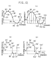
- Fig. 12(a) shows the concept for a conventional line density conversion.
- Plots 81 through 93 in Fig. 12(a) indicate the input values of the secondary density information.
- This example shows a reduction conversion by three fourths and points 84, 88 and 92 with cross marks on the plots are eliminated.
- various methods which not only eliminate but do so by taking into account the situation of peripheral pixels, are proposed under the present conditions.
- Fig. 12(b) shows an example in which density is determined by taking an average of the eliminated secondary density information and the next secondary density information.
- Plots 81' to 83' are of the same density as the input, but an average density of the plots 84 and 85 of input is set as an output density value of a plot 85'. It also applies to plots 89' and 93'. However, as operations are carried out only when elimination is generated in this method, undesirable patterns which were not in the original pixel can be generated depending on the combination of the space frequency of the input document, and the rate of enlargement or reduction.
- interpolation processing is carried out by executing the operation using multivalue data for each secondary density information.
- Fig. 12(c) shows as example of three fourths reduction as in Fig. 12(a). Secondary density information to be eliminated are not set here, but coordinate conversion as shown by a vertical line is carried out and the density at the above point is decided by the adjacent two dot pixel. This decision is made by a rectilinear distribution according to the distance from the above two dot pixels. Incidentally, it is possible to carry it out a through curvilinear assumption by increasing the number if reference points.
- Fig. 12(d) shows the density change after conversion. The difference from the conventional method cannot be known from the explanatory diagram of this Fig. 12, but as the reduction processing operation is carried out for each pixel in the processing method of this preferred embodiment, stable processing is possible, and it has the effect that the generation of undesirable patterns which occurred in the past is drastically reduced.
- Fig. 13 shows the line density conversion means 7 of this preferred embodiment.
- An output DS of the MTF correction means 5 is latched to a register 111 and then to a register 112 delayed for part of one pixel.
- the density values stored in these two registers 111 and 112 are processed in an interpolation means 113 to obtain the output DN.
- the interpolation means 113 the contents (density value) of register 111 and register 112 are multiplied by coefficients in multipliers 115 and 116 respectively, and an operation to add both the values is carried out in an adder 117.
- the coefficient at the multiplier 115 is determined in an interpolation coordinate operation part 122 by an operation where the interpolation position is located between the two reference pixels.
- the coefficient of the multiplier 116 is obtained by substracting the the coefficient value of the multiplier 116 from the complement of the coefficient value of the multiplier 115, namely, the value "1". This operation is carried out by an inverter 114.
- the interpolation coordinate operation part 122 comprises a register 118 in which the conversion rate DDA is set, a register 119 and an adder 120 which adds the contents of both the registers 118 and 119 and outputs them to the register 119 and a register 121, and the contents of the reister 121 are output to the adder 115.
- the conversion rate DDA corresponds to the distance between interpolation pixels, and is designated by a CPU (central processing unit), which is not illustrated. For example, when multiplied by K times, the value of 1/K is set at the register 118 in the adder 120. The contents of this register 118 are added to the contents of the register 119 in which the present coordinate value is stored, and how and to which of the two pixels, it is the close are directed.
- This addition result (coordinate value) is outputted to the register 121.
- Fig. 14 is a diagram of the binary coding processing according to this preferred embodiment.
- Fig. 14(a) shows two lines, of which the lower line 137 is being binary coded.
- the upper line 136 is the next line which will be binary coded.
- the secondary density information of the line 137 which are being binary coded those being binary coded presently are shown by pixel 134, those after binary coding by pixel 135, and those before binary coding by pixel 133.
- Simple binary coding can be executed by comparing the secondary density information, with the threshold value TH and by finding out which is larger.
- the error diffusion binary coding as mentioned in the document "An Adaptive Algorithm for Spatial Grey Scale" by R. Floyd et al, SID 75 DIGEST, p.
- the secondary density information Ro is compared with the threshold value TH, a density value So after binary coding is decided on, and then to what degree the difference is generated in the secondary density information before and after binary coding is performed. And the correction operation is carried out for the secondary density information which have not been binary coded (130, 131, 132 and 133 in the example of Fig. 14(a)) around it to correct the difference. This processing order is shown in Fig. 14(b).
- Fig. 15 shows the binary coding means 10 of this preferred embodiment.
- An output DN from the line density conversion means 7 is outputted to the error memory 9 (Fig. 3) as DN1 through registers with adders 141, 142 and 143.
- An output of the error memory 9 is also inputted as DN2.
- This inpput DN2 is put into an error diffusion means 145 through a register with adder 144.
- error correction means f2, f3, f4 and f1 by the binary coding are diffusively added to the registers 141, 142, 143 and 144 respectively.
- the error diffusion means 145 is shown in Fig. 16.
- a binary coding contrast input R output of the reigster 144) and the threshold value TH are compared in a comparator 146 to output a binary coding result DO.
- Simply binary coding can be executed by comparing the secondary density information R with the threshold value TH in the comparator 146 to output a binary coding result DO.
- the difference between this output DO and the input R is distributed using multipliers 149, 150, 151 and 152, and outputted to the registers with adders 141, 142, 143 and 144 (Fig. 15), and are added with each input to diffuse the error.
- Fig. 17 shows the facsimile device according to another preferred embodiment of the present invention.
- the above-mentioned superfine operation means 1 the window matrix 4, the MTF correction means 5, the zone judgement means 6, the line density conversion means 7 and the binary coding means 10 are integrated on one semiconductor chip 200, and a high-function one-chip memory 201 for a display such as a page memory is used instead of the line memories 2 and 3 to obtain a reduction of the data transfer time.
- Shift registers 202, 203, 204 and 205 in this high-function memory 201 are operated as outside line memories of the LSI 200 and operation results and data are also transferred from the shift registers 202 to 205 through a bus 207 by a RAM 206, and data transfer by a CPU 611 becomes unnecessary.
- the RAM 206 can be used as a line memory.
- Fig. 18 explains the recording operation of the recorder 615.
- the digital image signal at the encode/decode means 610 is directly transferred to the recorder 615.
- the digital image signal can be modified like in the embodiment shown in Fig. 18.
- Fig. 18(a) shows binary coded secondary density information to be recorded in the sub-scanning direction.
- Binary coded secondary density information 710, 711 indicate "BLACK”
- binary coded secondary density information 712, 713 indicate "WHITE”.
- Fig. 18(b) shows recording pixels on the recording material in the sub-scanning direction corresponding to the coded secondary density information 710, 711, 712 and 713.
- the recording pixel 701 corresponds to the binary coded pixel density information 710
- the recording pixel 702 corresponds to the binary coded secondary density information 711
- the recording pixel 703 corresponds to the binary coded secondary density information 712
- the recording pixel 704 corresponds to the binary coded secondary density information 713.
- Half of the pixel 702 to be recorded as "WHITE” is recorded as "BLACK” because half of the recording pixel of 703 overlaps half the recording pixel 702 recorded as "BLACK”.
- the binary coded secondary density information 711 is modified from "BLACK” to "WHITE” as shown in Fig. 18(c). So, the recording pixel 702 is recorded as "WHITE", as shown in Fig. 18(d).
- the recording pixels 702, 704 are represented having a gap in the main-scanning direction with regard to the portions 701, 703 for facilitating the explanation (can otherwise not be distinguished). There is no such gap in the embodiment. In another embodiment, such a gap can be in the main-scanning direction in Fig. 18(b) and Fig. 18(d).
- Fig. 18(e) shows the recording operation means having the function of the recording operation in the video signal processing means 608, preferably in the digital processor 507.
- the recording operation means comprises registers 721, 722, 723, line memories 724, 725, and logic operation means 726.
- Each of the registers 721, 722, 723 stores the binary coded secondary density information RA (e.g. 710), RB (e.g. 711), RC (e.g. 712) in the sub-scanning direction.
- the registers 721, 722 are connected through the line memory 724, and the registers 722, 723 are connected through the line memory 725.
- the logical operation means 726 is connected to the registers 721, 722, 723 and receives the output of each of the registers 721, 722, 723, and has a logical operation in the manner that if the binary coded secondary density information RA, RB indicate "BLACK” and RC indicates “WHITE", the binary coded secondary density information RB is modified from "BLACK” to "WHITE” as an output signal (RB').
- FIG. 19 shows an embodiment of a data processing system.
- a display means 801 such as a Cathode Ray Tube device (CRT) for displaying the secondary density information on the screen, includes an input means such as a keyboard.
- a display control means 802 such as an Advanced Cathode Ray Tube Controller (ACRTC), connected to the image bus B1, the image memory 609 and the display means 801, controls the operation of the display means 801.
- An optical disc 803 stores the coded secondary density information optically, and an optical disc controller 804 which is conntected between the optical disc 803 and the system bus B2, controls the operation of the optical disc 803.
- ACRTC Advanced Cathode Ray Tube Controller
- a hard disc 805 stores the coded secondary density information magnetically, and a hard disc controller 806 which is connected between the hard disc 805 and the sytem bus B2, controls the operation of the hard disc 805.
- a LAN interface means has the function for transmitting the coded secondary density information to the local area network 808 and for receiving the coded secondary density information from the local area network 808.
- a speech synthesis means 809 synthesizes sound on the basis of the coded secondary density information to output the sound through a loudspeaker 810.
- a speech recognition means 811 recognizes the user's speech through a microphone 812.
Landscapes
- Engineering & Computer Science (AREA)
- Multimedia (AREA)
- Signal Processing (AREA)
- Image Processing (AREA)
Claims (20)
- Bilddatenverarbeitungssystem, das folgendes aufweist:(a) eine Eingabeeinrichtung (INPUT), die zum Eingeben eines abgetasteten Bildsignals geeignet ist, das aus einer Folge von Bildpixeln besteht, von denen jedes einen primären Dichteinformationswert Xj (j = 1, 2, 3 ...) hat, wobei jedes j-te Pixel ein vorheriges (j-1)-tes Pixel um 1/n (n ≧ 2, n: ganze Zahl) eines Pixelabstands in wenigstens einer ersten Abtastrichtung räumlich überlappt;(b) eine Berechnungseinrichtung (1), die geeignet ist, sekundäre Dichteinformationswerte ΔXj in Bezug auf jedes Pixel gemäß der folgenden Beziehung zu berechnen, wobei ΔXj die Dichteinformation des Teils des j-ten Pixels darstellt, der das (j-1)-te Pixel nicht überlappt:

oder
n das Verhältnis der Breite in der vorbestimmten Richtung des Teils des j-ten Pixels, der das (j-1)-te Pixel nicht überlappt zu der Breite in der vorbestimmten Richtung des j-ten Pixels ist; und(c) eine Einrichtung, die geeignet ist, ein Ausgaangs-Bildsignal mit höherer Auflösung basierend auf den sekundären Dichteinformationswerten zu erzeugen. - Bilddatenverarbeitungssystem nach Anspruch 1, das weiterhin eine Speichereinrichtung (4) aufweist zum Speichern wenigstens eines der primären Dichteinformationswerten Xj und der sekundären Dichteinformationswerte ΔXj.
- Bilddatenverarbeitungssystem nach Anspruch 2, wobei die Eingabeeinrichtung (INPUT) die anfängliche primäre Dichteinformation X₀ als die anfängliche sekundäre Dichteinformation ΔX₀ empfängt.
- Bilddatenverarbeitungssystem nach einem der vorangehenden Ansprüche, wobei

- Bilddatenverarbeitungssystem nach einem der vorangehenden Ansprüche, das weiterhin eine Auswahleinrichtung (311, 312, 313) zum Auswählen eines Wertes für n aufweist.
- Bilddatenverarbeitungssystem nach einem der vorangehenden Ansprüche, das weiterhin eine MTF-Korrekturverarbeitungseinrichtung (5) und eine Zonen-Beurteilungsverarbeitungseinrichtung (6) aufweist.
- Bilddatenverarbeitungssystem nach Anspruch 6, wobei die MTF-Korrekturverarbeitungseinrichtung (5) und die Zonen-Beurteilungsverarbeitungseinrichtung (6) den in der Speichereinrichtung (4) gespeicherten sekundären Dichteinformationswert ΔXj benutzen.
- Bilddatenverarbeitungssystem nach Anspruch 7, das weiterhin eine Zeilendichte-Umwandlungsverarbeitungseinrichtung (7) und eine Binärcodier-Verarbeitungseinrichtung (10) aufweist.
- Bilddatenverarbeitungssystem nach Anspruch 8, wobei die MTF-Korrekturverarbeitungseinrichtung (5) und die Binärcodier-Verarbeitungseinrichtung (10) eine operationsmäßige Verarbeitung durch Ändern des Wertes ihrer eigenen Operationsparameter gemäß den Ergebnissen ausführen, die durch die Zonen-Beurteilungsverarbeitungseinrichtung (6) erhalten werden.
- Bilddatenverarbeitungssystem nach einem der Ansprüche 6 bis 9, wobei eine Beurteilungs-Parametereingabeeinrichtung zum Ausführen einer Zonentrennungsbestimmung durch den Benutzer in der Zonen-Beurteilungsverarbeitungseinrichtung (6) enthalten ist.
- Bilddatenverarbeitungssystem nach einem der Ansprüche 6 bis 10, wobei die MTF-Korrekturverarbeitungseinrichtung (5) eine Operationsverarbeitung durch Bezugnahme auf die sekundäre Dichteinformation, die zu bearbeiten ist, und die sekundäre Dichteinformation, die die zu bearbeitende sekundäre Dichteinformation umgibt, ausführt.
- Bilddatenverarbeitungssystem nach einem der Ansprüche 8 bis 11, wobei die Zeilendichte-Umwandlungsverarbeitungseinrichtung (7) mit einer Einrichtung zum Entscheiden über die Dichte der Interpolations-Sekundär-Dichteinformation auf der Basis des Abstands zwischen der Interpolations-Sekundär-Dichteinformation und der Referenz-Sekundär-Information ausgestattet ist.
- Bilddatenverarbeitungssystem nach einem der Ansprüche 8 bis 12, wobei die Binärcodier-Verarbeitungseinrichtung (10) mit einer Fehlerdiffundiereinrichtung (145) zum Steuern der Diffusion von Fehlern ausgestattet ist.
- Bilddatenverarbeitungssystem nach einem der Ansprüche 8 bis 13, wobei die Binärcodier-Verarbeitungseinrichtung (10) mit einer einfachen Binärcodier-Einrichtung und einer Fehlerdiffusions-Binärcodiereinrichtung (145) ausgestattet ist.
- Bilddatenverarbeitungssystem nach einem der Ansprüche 2 bis 14, das weiterhin eine weitere Speichereinrichtung (2, 3) aufweist, die mit der Speichereinrichtung (4) verbunden ist, zum Speichern des j-ten Sekundär-Dichteinformationswerts ΔXj.
- Bilddatenverarbeitungssystem nach einem der Ansprüche 6 bis 15, wobei die MTF-Korrekturverarbeitungseinrichtung (5) eine MTF-Korrekturoperation für eine Vielzahl von Sekundär-Dichteinformationen gleichzeitig ausführt.
- Bilddatenverarbeitungssystem nach einem der Ansprüche 6 bis 16, wobei die Zonen-Beurteilungsverarbeitungseinrichtung (6) zum Beurteilen, ob es eine Binärcodierzone oder eine Halbtonzone ist oder nicht, mit einer Anzahl von Sekundär-Dichteinformationen in der Hauptabtastrichtung ausgestattet ist, die größer als die Anzahl der Sekundär-Dichteinformationen in der Unterabtastrichtung ist.
- Bilddatenverarbeitungssystem nach Anspruch 17, wobei die Zonen-Beurteilungsverarbeitungseinrichtung (6) mit einer Speichereinrichtung (8) zum Speichern von Beurteilungsergebnissen bei einer vorherigen Zeile ausgestattet ist.
- Bilddatenverarbeitungssystem nach den Ansprüchen 17 bis 18, wobei die Zonen-Beurteilungsverarbeitungseinrichtung (6) eine OR-Verknüpfungseinrichtung enthält, zu der das Beurteilungsergebnis bei einer vorherigen Zeile und das Beurteilungsergebnis bei einer gegenwärtigen Zeile eingegeben werden, und die ein entsprechendes sekundäres Beurteilungsergebnis ausgibt.
- Bilddatenverarbeitungssystem nach einem der Ansprüche 2 bis 15, das in einem Halbleitersubstrat integriert ist.
Applications Claiming Priority (2)
| Application Number | Priority Date | Filing Date | Title |
|---|---|---|---|
| JP233530/88 | 1988-09-20 | ||
| JP23353088 | 1988-09-20 |
Publications (2)
| Publication Number | Publication Date |
|---|---|
| EP0362590A1 EP0362590A1 (de) | 1990-04-11 |
| EP0362590B1 true EP0362590B1 (de) | 1994-05-04 |
Family
ID=16956488
Family Applications (1)
| Application Number | Title | Priority Date | Filing Date |
|---|---|---|---|
| EP89117040A Expired - Lifetime EP0362590B1 (de) | 1988-09-20 | 1989-09-14 | Faksimilesystem |
Country Status (4)
| Country | Link |
|---|---|
| US (1) | US5566253A (de) |
| EP (1) | EP0362590B1 (de) |
| KR (1) | KR910007327A (de) |
| DE (1) | DE68915101T2 (de) |
Families Citing this family (5)
| Publication number | Priority date | Publication date | Assignee | Title |
|---|---|---|---|---|
| US5229760A (en) * | 1990-06-28 | 1993-07-20 | Xerox Corporation | Arithmetic technique for variable resolution printing in a ros |
| DE19605567A1 (de) * | 1996-02-15 | 1997-08-21 | Sel Alcatel Ag | Optisches frequenzkodiertes CDMA-Übertragungssystem und optischer Empfänger dafür |
| JP3261996B2 (ja) * | 1996-09-20 | 2002-03-04 | 松下電器産業株式会社 | 画像形成装置 |
| US7495669B2 (en) * | 2002-12-26 | 2009-02-24 | Canon Kabushiki Kaisha | Image processing apparatus and image processing method |
| EP1434419B1 (de) * | 2002-12-26 | 2009-05-27 | Canon Kabushiki Kaisha | Bildverarbeitungsapparatur und Bildverarbeitungsverfahren |
Citations (1)
| Publication number | Priority date | Publication date | Assignee | Title |
|---|---|---|---|---|
| US32291A (en) * | 1861-05-14 | Henry s |
Family Cites Families (10)
| Publication number | Priority date | Publication date | Assignee | Title |
|---|---|---|---|---|
| US4084183A (en) * | 1970-03-18 | 1978-04-11 | Dr. Ing. Rudolf Hell Gmbh. | Method for the electro-optical reproduction of half-tone pictures |
| JPS587109B2 (ja) * | 1974-09-09 | 1983-02-08 | ケイディディ株式会社 | フアクシミリシンゴウ ノ ジヨウホウヘンカガソアドレスフゴウカホウシキ |
| JPS5954376A (ja) * | 1982-09-21 | 1984-03-29 | Konishiroku Photo Ind Co Ltd | 画像処理方法 |
| GB2129652B (en) * | 1982-10-27 | 1986-06-04 | Matsushita Electric Ind Co Ltd | Method and apparatus for processing image signal |
| JPS61203785A (ja) * | 1985-03-07 | 1986-09-09 | Dainippon Screen Mfg Co Ltd | 2値画像デ−タの平滑化処理方法及びその装置 |
| US4686698A (en) * | 1985-04-08 | 1987-08-11 | Datapoint Corporation | Workstation for interfacing with a video conferencing network |
| US4717962A (en) * | 1986-12-17 | 1988-01-05 | Kabushiki Kaisha Toshiba | Method for compressing and reconstructing a data representation of a picture |
| US4797942A (en) * | 1987-03-02 | 1989-01-10 | General Electric | Pyramid processor for building large-area, high-resolution image by parts |
| EP0327107B1 (de) * | 1988-02-05 | 1994-07-13 | Dainippon Screen Mfg. Co., Ltd. | Bildschärfeverbesserungsverfahren und -prozessor für Bildreproduktion mit Abtaster |
| US5153749A (en) * | 1988-09-01 | 1992-10-06 | Canon Kabushiki Kaisha | Image encoding apparatus |
-
1989
- 1989-09-14 DE DE68915101T patent/DE68915101T2/de not_active Expired - Fee Related
- 1989-09-14 EP EP89117040A patent/EP0362590B1/de not_active Expired - Lifetime
- 1989-09-20 KR KR1019890013533A patent/KR910007327A/ko not_active Application Discontinuation
-
1992
- 1992-07-27 US US07/920,177 patent/US5566253A/en not_active Expired - Fee Related
Patent Citations (1)
| Publication number | Priority date | Publication date | Assignee | Title |
|---|---|---|---|---|
| US32291A (en) * | 1861-05-14 | Henry s |
Also Published As
| Publication number | Publication date |
|---|---|
| DE68915101T2 (de) | 1994-09-15 |
| EP0362590A1 (de) | 1990-04-11 |
| KR910007327A (ko) | 1991-04-30 |
| US5566253A (en) | 1996-10-15 |
| DE68915101D1 (de) | 1994-06-09 |
Similar Documents
| Publication | Publication Date | Title |
|---|---|---|
| US6324309B1 (en) | Image processing apparatus | |
| JP4912270B2 (ja) | 画像処理装置及びその制御方法 | |
| US9215345B2 (en) | Method and system for inverse halftoning utilizing inverse projection of predicted errors | |
| EP1542447B1 (de) | Bilddatenverarbeitungseinrichtung, bilddatenverarbeitungsverfahren, programm, aufzeichnungsmedium und bildleseeinrichtung | |
| EP1058448B1 (de) | Bildverarbeitungsgerät | |
| EP0362590B1 (de) | Faksimilesystem | |
| US6636649B1 (en) | Image processing apparatus and the method of correcting the inclination | |
| JP3311549B2 (ja) | 画像処理装置の変倍制御装置 | |
| JP4861506B2 (ja) | 画像処理装置およびその制御方法 | |
| JP3386203B2 (ja) | 画情報の処理方法及び画情報処理装置 | |
| JP2658897B2 (ja) | 画像読み取り装置及びそれを用いたファクシミリ装置 | |
| JP4068769B2 (ja) | 画像処理装置及びその傾き補正方法 | |
| JP2555199B2 (ja) | 画像読み取り方法 | |
| JP3212339B2 (ja) | 画像変倍装置 | |
| JP3858877B2 (ja) | 画像形成装置及び画像形成方法 | |
| JP3124839B2 (ja) | 画像形成装置 | |
| JP2945022B2 (ja) | 画像処理装置 | |
| KR910002773B1 (ko) | 의사중간조 화상 데이터의 데이터 압축 및 복원방법 | |
| JP2755506B2 (ja) | 画像形成装置 | |
| JP2002101303A (ja) | 画像処理装置 | |
| JPH10262148A (ja) | 画像処理装置 | |
| JPH0158713B2 (de) | ||
| JPH06217114A (ja) | 中間調画像処理装置 | |
| JPH0955850A (ja) | 疑似中間調画像処理装置 | |
| JPH06311346A (ja) | 画像処理装置 |
Legal Events
| Date | Code | Title | Description |
|---|---|---|---|
| PUAI | Public reference made under article 153(3) epc to a published international application that has entered the european phase |
Free format text: ORIGINAL CODE: 0009012 |
|
| 17P | Request for examination filed |
Effective date: 19890914 |
|
| AK | Designated contracting states |
Kind code of ref document: A1 Designated state(s): DE FR GB IT |
|
| 17Q | First examination report despatched |
Effective date: 19921105 |
|
| GRAA | (expected) grant |
Free format text: ORIGINAL CODE: 0009210 |
|
| AK | Designated contracting states |
Kind code of ref document: B1 Designated state(s): DE FR GB IT |
|
| REF | Corresponds to: |
Ref document number: 68915101 Country of ref document: DE Date of ref document: 19940609 |
|
| ITF | It: translation for a ep patent filed | ||
| ET | Fr: translation filed | ||
| PLBE | No opposition filed within time limit |
Free format text: ORIGINAL CODE: 0009261 |
|
| STAA | Information on the status of an ep patent application or granted ep patent |
Free format text: STATUS: NO OPPOSITION FILED WITHIN TIME LIMIT |
|
| 26N | No opposition filed | ||
| REG | Reference to a national code |
Ref country code: GB Ref legal event code: IF02 |
|
| PGFP | Annual fee paid to national office [announced via postgrant information from national office to epo] |
Ref country code: FR Payment date: 20020822 Year of fee payment: 14 |
|
| PGFP | Annual fee paid to national office [announced via postgrant information from national office to epo] |
Ref country code: GB Payment date: 20020827 Year of fee payment: 14 |
|
| PGFP | Annual fee paid to national office [announced via postgrant information from national office to epo] |
Ref country code: DE Payment date: 20020916 Year of fee payment: 14 |
|
| PG25 | Lapsed in a contracting state [announced via postgrant information from national office to epo] |
Ref country code: GB Free format text: LAPSE BECAUSE OF NON-PAYMENT OF DUE FEES Effective date: 20030914 |
|
| PG25 | Lapsed in a contracting state [announced via postgrant information from national office to epo] |
Ref country code: DE Free format text: LAPSE BECAUSE OF NON-PAYMENT OF DUE FEES Effective date: 20040401 |
|
| GBPC | Gb: european patent ceased through non-payment of renewal fee |
Effective date: 20030914 |
|
| PG25 | Lapsed in a contracting state [announced via postgrant information from national office to epo] |
Ref country code: FR Free format text: LAPSE BECAUSE OF NON-PAYMENT OF DUE FEES Effective date: 20040528 |
|
| REG | Reference to a national code |
Ref country code: FR Ref legal event code: ST |
|
| PG25 | Lapsed in a contracting state [announced via postgrant information from national office to epo] |
Ref country code: IT Free format text: LAPSE BECAUSE OF NON-PAYMENT OF DUE FEES Effective date: 20050914 |