EP0357423B1 - Dispositif d'exposition - Google Patents
Dispositif d'exposition Download PDFInfo
- Publication number
- EP0357423B1 EP0357423B1 EP89308821A EP89308821A EP0357423B1 EP 0357423 B1 EP0357423 B1 EP 0357423B1 EP 89308821 A EP89308821 A EP 89308821A EP 89308821 A EP89308821 A EP 89308821A EP 0357423 B1 EP0357423 B1 EP 0357423B1
- Authority
- EP
- European Patent Office
- Prior art keywords
- exposure
- flow
- rate
- temperature
- chuck
- Prior art date
- Legal status (The legal status is an assumption and is not a legal conclusion. Google has not performed a legal analysis and makes no representation as to the accuracy of the status listed.)
- Expired - Lifetime
Links
Images


Classifications
-
- G—PHYSICS
- G03—PHOTOGRAPHY; CINEMATOGRAPHY; ANALOGOUS TECHNIQUES USING WAVES OTHER THAN OPTICAL WAVES; ELECTROGRAPHY; HOLOGRAPHY
- G03F—PHOTOMECHANICAL PRODUCTION OF TEXTURED OR PATTERNED SURFACES, e.g. FOR PRINTING, FOR PROCESSING OF SEMICONDUCTOR DEVICES; MATERIALS THEREFOR; ORIGINALS THEREFOR; APPARATUS SPECIALLY ADAPTED THEREFOR
- G03F7/00—Photomechanical, e.g. photolithographic, production of textured or patterned surfaces, e.g. printing surfaces; Materials therefor, e.g. comprising photoresists; Apparatus specially adapted therefor
- G03F7/70—Microphotolithographic exposure; Apparatus therefor
- G03F7/708—Construction of apparatus, e.g. environment aspects, hygiene aspects or materials
- G03F7/70858—Environment aspects, e.g. pressure of beam-path gas, temperature
- G03F7/709—Vibration, e.g. vibration detection, compensation, suppression or isolation
-
- G—PHYSICS
- G03—PHOTOGRAPHY; CINEMATOGRAPHY; ANALOGOUS TECHNIQUES USING WAVES OTHER THAN OPTICAL WAVES; ELECTROGRAPHY; HOLOGRAPHY
- G03F—PHOTOMECHANICAL PRODUCTION OF TEXTURED OR PATTERNED SURFACES, e.g. FOR PRINTING, FOR PROCESSING OF SEMICONDUCTOR DEVICES; MATERIALS THEREFOR; ORIGINALS THEREFOR; APPARATUS SPECIALLY ADAPTED THEREFOR
- G03F7/00—Photomechanical, e.g. photolithographic, production of textured or patterned surfaces, e.g. printing surfaces; Materials therefor, e.g. comprising photoresists; Apparatus specially adapted therefor
- G03F7/70—Microphotolithographic exposure; Apparatus therefor
- G03F7/70691—Handling of masks or workpieces
- G03F7/707—Chucks, e.g. chucking or un-chucking operations or structural details
-
- G—PHYSICS
- G03—PHOTOGRAPHY; CINEMATOGRAPHY; ANALOGOUS TECHNIQUES USING WAVES OTHER THAN OPTICAL WAVES; ELECTROGRAPHY; HOLOGRAPHY
- G03F—PHOTOMECHANICAL PRODUCTION OF TEXTURED OR PATTERNED SURFACES, e.g. FOR PRINTING, FOR PROCESSING OF SEMICONDUCTOR DEVICES; MATERIALS THEREFOR; ORIGINALS THEREFOR; APPARATUS SPECIALLY ADAPTED THEREFOR
- G03F7/00—Photomechanical, e.g. photolithographic, production of textured or patterned surfaces, e.g. printing surfaces; Materials therefor, e.g. comprising photoresists; Apparatus specially adapted therefor
- G03F7/70—Microphotolithographic exposure; Apparatus therefor
- G03F7/70691—Handling of masks or workpieces
- G03F7/70716—Stages
-
- G—PHYSICS
- G03—PHOTOGRAPHY; CINEMATOGRAPHY; ANALOGOUS TECHNIQUES USING WAVES OTHER THAN OPTICAL WAVES; ELECTROGRAPHY; HOLOGRAPHY
- G03F—PHOTOMECHANICAL PRODUCTION OF TEXTURED OR PATTERNED SURFACES, e.g. FOR PRINTING, FOR PROCESSING OF SEMICONDUCTOR DEVICES; MATERIALS THEREFOR; ORIGINALS THEREFOR; APPARATUS SPECIALLY ADAPTED THEREFOR
- G03F7/00—Photomechanical, e.g. photolithographic, production of textured or patterned surfaces, e.g. printing surfaces; Materials therefor, e.g. comprising photoresists; Apparatus specially adapted therefor
- G03F7/70—Microphotolithographic exposure; Apparatus therefor
- G03F7/708—Construction of apparatus, e.g. environment aspects, hygiene aspects or materials
- G03F7/70858—Environment aspects, e.g. pressure of beam-path gas, temperature
- G03F7/70866—Environment aspects, e.g. pressure of beam-path gas, temperature of mask or workpiece
- G03F7/70875—Temperature, e.g. temperature control of masks or workpieces via control of stage temperature
Definitions
- the present invention relates to an exposure apparatus wherein a predetermined radiation energy is applied to a wafer through a mask, by which a pattern of the mask is printed on the wafer, more particularly to an exposure apparatus having a wafer chuck for maintaining the wafer at a predetermined fixed position, equipped with a temperature control system.
- a temperature control cooling medium is flown through the wafer chuck so as to maintain a constant temperature of the wafer during the exposure and to prevent thermal deformation.
- the flow rate was constant to suppress the temperature rise resulting from the wafer exposure.
- the rate of the cooling medium is flown through the passage in the wafer chuck, the wafer chuck and the wafer supporting portion therearound vibrates to flow of the medium.
- the displacement resulting from the vibration is large as several tens x 10 ⁇ 3 microns - several hundreds x 10 ⁇ 3 microns. Such a large vibration during the exposure operation, degrades the precision of the pattern formation by the exposure.
- the apparatus of the present invention is provided with flow control means in the medium passage, which is operated in accordance with operation of the exposure apparatus.
- the control is such that during the exposure operation, the vibration resulting from the flow does not influence the pattern formation precision, and during non-exposure-operation, the temperature rise is sufficiently absorbed.
- Figure 1 is a schematic drawing of an exposure apparatus according to an embodiment of the present invention.
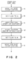
- Figure 2 is a flow chart illustrating an operational sequence of the apparatus of Figure 1.
- Figure 3 is a timing chart illustrating operation of the apparatus of Figure 1 embodiment.
- Figure 4 shows an exposure apparatus according to another embodiment of the present invention.
- Figure 5 shows an exposure apparatus according to a yet further embodiment of the present invention.
- Figure 6 shows a wafer chuck used in the apparatus of Figure 5 embodiment.
- Figure 7 is a timing chart illustrating operation of the apparatus of Figure 5.
- Figure 8 is a top plan view of a wafer showing an order of exposure operations.
- Figure 9 shows another example of the wafer chuck.
- the exposure apparatus comprises a radiation source in the form of, for example, an extra-high pressure mercury lamp, and excimer laser source, a soft-X-ray source or the like, a shutter 2 for controlling the exposure, a wafer chuck 5 for attracting and maintaining at a predetermined exposure position a wafer 4 onto which a pattern of a mask is to be exposure-transferred, a positioning stage 6 for moving and positioning the wafer chuck 5 for aligning sequentially the respective shot areas of the wafer 4 relative to the mask 3, a flow control valve 7 for controlling the flow of a temperature controlling medium, a flow passage 8 for flowing the temperature controlling medium for controlling the temperature of the wafer chuck 5, and a temperature controlling pump 8 for circulating the medium.
- a radiation source in the form of, for example, an extra-high pressure mercury lamp, and excimer laser source, a soft-X-ray source or the like
- a shutter 2 for controlling the exposure
- a wafer chuck 5 for attracting and maintaining at a predetermined exposure position a wa
- the apparatus further comprises a flow controller for controlling the flow controlling valve 7, an exposure controller 11 for supplying control instructions to the radiation source 1, the shutter 2, the stage 6 and the flow controller 10 and others to control the entire apparatus particularly in the process of exposure steps, outlet 12 and inlet 13 for the temperature controlling medium in the wafer chuck 5, and a signal line 14 for supplying from the exposure controller 11 to the flow controller 10 a signal indicative of the operational stage in the exposure sequential operation, more particularly, whether or not the exposure apparatus is performing the exposure operation.
- the cooling medium is fed out by the pump 9.
- the temperature of the medium is controlled within the temperature range of 23 °C ⁇ 2/100 °C, and is recirculated.
- the cooling medium flows through the passage 8 and the inlet 13 into the wafer chuck 5, where it absorbs the heat from the wafer chuck 5 and the wafer 4, and it is discharged through the outlet 12.
- the discharged medium is returned through the flow control valve 7, and is again temperature-controlled to be 20 °C ⁇ 2/100 °C. Then, the medium repeats the circulation.
- the exposure controller 11 transmits through the signal line 14 to the flow controller 10 a signal indicative of whether the apparatus is going to start the exposure operation or is going to end the exposure operation.
- the flow controller 10 includes a two-rate flow controlling valve 7, the flow rate is switched in accordance with the signal.
- the flow control valve 7 controls during the exposure the flow rate to be A with which the vibration of the wafer chuck 5 is within a tolerable range so as not to influence the pattern formation precision.
- the flow is B (A ⁇ B), by which the temperature rise resulting from the accumulation of the exposure energy applied to the wafer 4 and the wafer chuck 5 by the previous exposure or exposures is suppressed within a tolerable range.
- the flow rate A may be zero, but it is preferably not zero, so that a certain degree of the heat is removed from the wafer chuck 5 during the exposure operation, within a limit of the resultant vibration not influencing the pattern formation precision.
- the exposure controller 11 in accordance with a sequence programmed beforehand, controls the radiation source 1, the opening and closing of the shutter 2 and movement of the positioning stage 6.
- FIG 2 there is shown a flow chart of the exposure operation sequence in the exposure apparatus described above.
- the exposure controller 11 drives the positioning stage 6 to align a first shot area of the wafer 4 to the exposure position, more particularly, relative to the mask 3 (step a ) in order to transfer the pattern of the mask 3 onto the first shot area of the wafer 4 which is already carried and attracted on the wafer chuck 5.
- the flow controller 10 sets the degree of opening of the flow controlling valve 7 to change the flow rate from B to A (step b).
- the shutter 2 is opened to effect the exposure of the first shot area (step c ).
- the shutter 2 closed, by which the first shot area exposure operation is completed at the point of time t3 (step d).
- the flow controller 10 sets the degree of opening of the flow control valve 7 back to the flow rate B (step e).
- a second shot area is aligned to the exposure position (step f), the exposure sequence operation for the second shot area is started.
- the above-described steps b, c, d and e are repeated; and further, the exposure for a third shot area is similarly controlled.
- FIG 3 (a) - (d) are time charts showing the temperature, the flow rate, the stage of exposure and amplitude of the vibration of the exposure apparatus with time.
- the flow rate is increased to B to decrease the temperature.
- Figure 4 shows an apparatus according to another embodiment of the present invention, wherein a temperature sensor 15 for sensing the temperature of the wafer chuck 5 is additionally provided. Also, added is a signal line 16 for transmitting the detected temperature to the flow controller 10.
- the flow controller 10 is responsive to the temperature of the wafer chuck 5 at the point of time t3, for example, of Figure 3 which is after the exposure operation to select the degree of the opening of the flow control valve 7 from multi-levels selectable, more particularly, so that the flow rate B during the non-exposure-operation to be one of B1, B2 ..., Bn (B1 ⁇ B2 ⁇ ... ⁇ Bn).
- the flow rate is controlled to be Bn to remove a greater amount of heat from the wafer chuck 5, and if the temperature is not so high, the flow rate may be B1, where B1 may be equal to A. If the temperature is between the above two, one of the flow rates B2, B3, ..., B(n-1) is selected in accordance with the level of the detected temperature.
- Bn the flow rate
- B2 B3, ..., B(n-1) is selected in accordance with the level of the detected temperature.
- the time period T shown in Figure 3 may be reduced as compared with the case where the flow rate is changed from Bn to A, therefore, it is preferable.
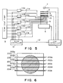
- Figure 5 shows an exposure apparatus according to a further embodiment of the present invention, wherein the exposure apparatus comprises a radiation source 1 for the exposure, and a shutter 2 for controlling the exposure.
- Designated by reference numerals 3 and 4 are a mask having a pattern to be transferred and a wafer on which the pattern of the mask 3 is to be transferred.
- the apparatus further comprises a wafer chuck 5 for attracting the wafer 4 and maintaining it at an unshown exposure position, a positioning stage 6 for sequentially positioning shot areas of the wafer 4 relative to the mask 3, an exposure controller 11 for controlling the exposure process steps, a flow controller 10 for controlling flow control valves 110a - 110e, a temperature control pump for circulating the temperature controlling medium and heat exchanger means not shown to control the medium temperature to be constant.
- the flow control valves 110a, 110b, 110c, 110d and 110e control the rate of flow therethrough.
- the temperature controlling medium flows through pipes 111a, 111b, 111c, 111d and 111e.
- a signal line 112 is effective to transmit the state of exposure operation or the exposure position from the exposure controller 107 to the flow controller 108.
- a temperature sensor 113 monitors the temperature of the wafer chuck.
- FIG. 6 shows details of the wafer chuck 5 used in this embodiment.
- a flow passage 203a is provided with an inlet 201a communicating with the pipe 111a.
- flow passages 203b - 203e are provided with respective inlets 201b - 201e communicating with the pipes 111b - 111e, respectively.
- the flow passage 203a is also provided with an outlet 202a.
- the flow passages 203b - 203e are provided with outlets 202b - 202e, respectively.
- Figure 7 is a timing chart illustrating operations of the apparatus of this embodiment.
- reference (a) shows whether the exposure apparatus is performing the exposure operation or not
- reference (b) shows the shot area of the wafer surface which is being exposed
- reference (c) shows the flow rate of the temperature controlling medium flowing through the pipe 111a.
- the references (d) - (g) designate the flow rates through the pipes 111b - 111e.
- the change of the flow rate is effected, taking the time period T into account, as shown in Figure 3(b).
- Figure 8 shows the order of exposure for the shot areas of the wafer 4 in this embodiment.
- a reference numeral 401 designates an area which can be exposed by one exposure, the same applies to the other areas.
- the temperature control medium is fed out of the temperature control pump 109 in Figure 5.
- the temperature of the medium is controlled to be within the range of 23 °C +2/100 °C and is circulated repeatedly.
- the pump 9 supplies the temperature controlling mediums to the five lines of the pipes 111a - 111e.
- the first line extends from the temperature control pump 9 to the pipe 111a. Through this line, the medium absorbs the heat from the wafer chuck 5 and the wafer 4, and is returned to the temperature control pump through the flow rate control valve 110a, and is again controlled in its temperature to be within the range of 2 °C ⁇ 2/100 °C.
- the second line is constituted by the pipe 111b and the flow rate control valve 110b.
- the third, fourth and fifth lines are constituted by the pipe 111c and the control valve 110c, by the pipe 110 and the control valve 110d, and by the pipe 111e and the control valve 110e, respectively.
- the exposure controller 11 through the signal line 112, supplies the exposure information representing whether the apparatus is going to start the exposure operation or whether it is terminating the exposure operation, and exposure position information representing what shot area of the wafer 4 is being exposed, to the flow controller 10.
- the exposure controller 11 has lay-out data representing how the wafer 4 is divided into shot areas. During the exposure operation, it discriminates the exposure shot on the basis of the lay-out data.
- the exposure information is produced on the basis of the starting and ending signals of the step-movement of the wafer 4 by the stage 6. This can be discriminated on the basis of an ending signal representing the completion of the alignment between the shot area of the wafer 4 and the mask pattern, or on the basis of the starting signal of the shutter 102 operation. In the latter case, however, the flow change by actuation of the valves 110a - 110e is to be quickly completed.
- the flow controller 10 controls the flow rate control valve 110a - 110e in accordance with the exposure information and the exposure position information described above, so as to control the rate of the temperature control medium in three stages (STD, L1 and L2 where STD > L1 > L2).
- the exposure controller 11 leads the wafer chuck 5 temperature from the temperature sensor 113 to predict the temperature of the wafer 4.
- the exposure controller 11 supplies the temperature of the wafer chuck described above or the temperature of the wafer 4 predicted, to the flow controller 10.
- the flow controller makes a correction of the flow rate from a basic or standard rate STD ( Figure 7) which has been predetermined, in accordance with the temperature information.
- the exposure controller 11 operates the positioning stage 6 by an unshown driving mechanism to align a first shot area of the wafer 4 with the mask 3 in order to expose the first shot area of the wafer 4 attracted on the wafer chuck 5 to the pattern of the mask 3. Then, the exposure controller 11 operates an unshown shutter driving mechanism to open the shutter 2 to start the exposure of the first shot area. After a predetermined period of time elapses, or after the predetermined exposure amount is reached, the shutter 2 is closed to complete the first shot area exposure operation.
- the positioning stage 6 is driven to align a second shot area of the wafer 4 relative to the mask 3, and then, similarly to the above-described first shot case, the exposure operation is performed.
- the third and fourth shot areas are sequentially subjected to the aligning and exposure operations until all the shot areas are exposed.
- the flow controller controls the valve 110a to provide the flow rate L1 in the passage 203a, the flow rate L1 is being the one to be set during the exposure operation being performed.
- the flow controller 10 sets the flow rate STD for the passage 203a by the valve 110a.
- the other passages 203b - 203e are similarly controlled, if any is adjacent to the currently exposed shot.
- the flow rate L1 and STD satisfy: STD > L1.
- the exposure shot comes to, or to the neighborhood of, the flow passage 203e.
- the flow rate through the passage 203a becomes L2 during the exposure operation.
- the exposure operation is not performed, it is STD.
- Figure 8 shows the order of exposure step. They are exposed in the order of a1, a2, a3, b1, b2, b3, b4, b5, c1, c2, c3, c4, c5, d1, d2, d3, d4, d5, e1, e2 and e3.
- This is one of typical order, but is not limiting.
- the surface of the wafer is shown as being divided into 21 square areas, but this is not limiting, either.
- Figure 7 is a timing chart illustrating above described operations.
- the flow rates of the passages 203a, 203b, 203c, 203d and 203e are all set to the STD.
- the flow rate of the passage 203a is set to be L1 before the start of the exposure operation for the shot area a1.
- the flow rates of the other passages 203b - 203e are L2.
- the flow rates L1, L2 and STD satisfy STD > L1 > L2, and therefore, the total flow of the medium supplied to the entire wafer chuck 5 is decreasing, and the flow rate of the passage 203a adjacent to the exposed shot area a1 is higher than those of the passages 203b - 203e. Therefore, the vibration of the wafer chuck 5 is decreased, and simultaneously, the temperature rise adjacent to the shot area a1 can be suppressed during the exposure operation to a certain extent.
- the flow rates of all of the passages 203a - 203e are returned to be STD, and the alignment operation for the next shot area a2 is started.
- the flow rate of the passage 203a returns to L1 before the start of the exposure operation of the shot area a2 after the completion of the alignment for the shot area a2.
- the flow rates of the passages 203b - 203e are again L2.
- the exposure operations of the shot areas a2 and a3 are completed, and the flow rates of the passages 203a - 203e are at this point of time are STD.
- the alignment of the shot area b1 is started.
- the flow rate of the passages 203a - 203e are all STD.
- the flow rate of the passage 203b becomes L1 prior to the start of the exposure after completion of the alignment for the shot area b1, and the flow rate of the other passages 203a, 203c - 203e are all L2.
- the flow rate of all of the flow passages 203a - 203e are standard. In the similar manner, the exposure sequential operation are performed.
- the flow rate of the liquid passage faced to the exposure shot area and the flow rate of the passage faced to the other shot areas satisfy STD > L1 > L2, when the temperature of the chuck 5 is controlled.
- STD > L1 > L2 when the temperature of the chuck 5 is controlled.
- the liquid (medium) supply to the position other than the exposure shot area is stopped, whereas the rate of flow which does not result in production of the vibration influential to the exposure operation is supplied only to the flow passage corresponding to the exposure shot area.
- the relationship is not limited to STD > L2, but STD ⁇ L2 is satisfactory.
- Figure 9 shows an apparatus according to a yet further embodiment of the present invention, wherein the flow passage 501 of the wafer chuck 5 is further divided finely, wherein the flow rates of the temperature controlling medium are controlled.
- the flow rate control means is provided to control the flow of the temperature controlling medium through the wafer chuck is provided, and therefore, the flow of the medium can be controlled in accordance with the state of exposure operation. Accordingly, the temperature of the wafer can be maintained within a predetermined tolerable range without reducing the throughput of the exposure process; and the possible degrading of the pattern formation precision due to the vibration stemming from the flow of the medium can be prevented, thus accomplishing the high precision patterning.
Claims (20)
- Procédé de formation précise de motifs, dans lequel un élément (4) est supporté par un plateau de serrage (5), l'élément (4) est exposé à un rayonnement afin d'y définir des motifs précis et un milieu thermostaté est mis en circulation à travers ledit plateau de serrage (5) pour supprimer l'augmentation de la température du plateau de serrage (5) et de l'élément supporté (4), lequel procédé est caractérisé en ce que le débit (A, B; STD, L1, L2), c'est-à-dire la quantité dudit milieu par unité de temps passant à travers ledit plateau de serrage (5), est inférieur (A; L1) durant l'exposition, moyen grâce auquel les vibrations sont abaissées à un niveau tolérable durant l'exposition, ce qui améliore la précision des motifs tout en supprimant l'augmentation de température dans la mesure où la température est contrainte de se situer dans un intervalle tolérable.
- Procédé selon la revendication 1, dans lequel la position du plateau de serrage (5) est modifiée après une exposition et avant une exposition suivante, et le débit (B; STD) est abaissé directement (A; L1, L2) à la suite du réalignement du plateau de serrage (5) qui précède l'exposition suivante.
- Procédé selon la revendication 1, dans lequel l'exposition est commencée par l'ouverture d'un obturateur (2) situé sur le trajet du rayonnement vers ledit élément (4) et le débit (B; STD) est abaissé directement (A; L1, L2) et rapidement à la suite de l'ouverture de l'obturateur (2).
- Procédé selon la revendication 1, dans lequel la température du plateau de serrage est détectée, et le débit, qui a augmenté (Bn) après la fin de l'exposition, a diminué (B1, B2, ...) en fonction de la température du plateau de serrage détectée, ou d'une température d'élément prévue sur laquelle il est basé, avant une exposition suivante.
- Procédé selon la revendication 4, dans lequel le débit (Bn à B2) a diminué en fonction de la température du plateau de serrage détectée, ou d'une température d'élément prévue, comme mentionné ci-dessus, depuis un niveau multiple (Bn, Bn-1, ..B2) à un autre (Bn-1, ..B1).
- Procédé selon la revendication 1, dans lequel le milieu thermostaté est mis en circulation à travers une pluralité de passages (203a à 203e) à travers ledit plateau de serrage (5), le débit (STD, L1, L2) dans chaque passage (203a à 203e) est commandé indépendamment et la quantité totale par unité de temps du milieu thermostaté passant à travers le plateau de serrage (5) est tel qu'il ne génère pas de vibrations interférant avec l'exposition tandis qu'une quantité de chaleur suffisante, à la position d'exposition de l'élément (4), est éliminée afin de supprimer une augmentation de température au-delà de l'intervalle tolérable.
- Procédé selon la revendication 6, dans lequel le débit (A, B; STD, L1, L2) du milieu thermostaté passant à travers le passage (203a, ..., 203e) le plus proche de la position exposée (a1, a2, ..., a3) de l'élément (4) est inférieur (A, L1, L2) pendant l'exposition à ce qu'il est après l'exposition (B ; STD).
- Procédé selon la revendication 7, dans lequel le débit (STD, L2) du milieu thermostaté passant à travers chaque passage (203b,...,203e; 203c, ...203a; ...) différent du passage (203a; 203b; ...) le plus proche de la position exposée (a1, a2, a3; b1, ..., b5; ...) est encore plus bas durant l'exposition que le débit (L1) à travers le passage (203a; 203b; ...) le plus proche de la position exposée (al, a2, a3; b1, ..., b5; ...).
- Procédé selon l'une quelconque des revendications précédentes 6 à 8, dans lequel le débit (STD) de chaque passage (203a à 203b) suivant une exposition est corrigé en fonction de la température du plateau de serrage.
- Appareil d'exposition pour définir des motifs précis dans un élément (4), lequel appareil comprend:
un plateau de serrage (5) pour supporter l'élément (4);
des moyens d'exposition (1 à 3, 6) pour exposer l'élément (4); et
des moyens d'alimentation (9) pour alimenter ledit plateau de serrage (5) en un milieu thermostaté par l'intermédiaire de moyens de passage d'écoulement (8, 203a à 203e; 501) présents dans le plateau de serrage;
lequel appareil d'exposition est caractérisé par:
des moyens de commande de débit (7; 110a à 110e) pour commander le débit (A, B; STD, L1, L2) du milieu thermostaté passant à travers lesdits moyens de passage d'écoulement (8, 203a à 203e; 501); et
un contrôleur de débit (10) qui est disposé pour commander l'opération desdits moyens de commande de débit (7; 110a à 110e) et qui fonctionne en fonction de l'opération d'exposition de façon que le débit (A, B; STD, L1, L2) du milieu thermostaté est inférieur (A; L1, L2) durant l'exposition, et en conséquence les vibrations sont abaissées durant l'exposition, ce qui améliore la précision des motifs tout en maintenant, cependant, la température du plateau de serrage dans un intervalle tolérable. - Appareil d'exposition selon la revendication 10, comprenant un contrôleur d'exposition (11) pour commander la chronologie de l'exposition, ledit contrôleur de débit (10) étant sensible aux signaux délivrés par ledit contrôleur d'exposition (11).
- Appareil d'exposition selon la revendication 11, comprenant des moyens à étages (6) pour déplacer ledit plateau de serrage (5) d'une position d'exposition (a1, a2, ..., e3) à une autre position d'exposition (a2, a3, ...), ledit contrôleur d'exposition (11) fonctionnant pour commander le fonctionnement desdits moyens à étages (6), et ledit contrôleur de débit (10) étant sensible audit contrôleur d'exposition (11) afin d'abaisser le débit (B; STD) lorsque la fin du réalignement dudit plateau de serrage (5) qui suit le mouvement vers la position d'exposition suivante (a, a3, ...), est signalée.
- Appareil d'exposition selon la revendication 11, comprenant un obturateur (2) disposé pour intercepter le rayonnement dirigé vers l'élément (4), ledit contrôleur d'exposition (11) fonctionnant pour commander le fonctionnement dudit obturateur (2), et ledit contrôleur de débit (10) étant sensible audit contrôleur d'exposition (11) afin d'effectuer un abaissement rapide du débit (B; STD) lorsque l'ouverture de l'obturateur (2) est signalée.
- Appareil d'exposition selon la revendication 10, comprenant un capteur de température de plateau de serrage (15), ledit contrôleur de débit (10) étant sensible à ce capteur durant la période de temps qui suit l'exposition afin de diminuer le débit (Bn, Bn-1, ...) en fonction de l'abaissement de la température.
- Appareil d'exposition selon la revendication 14, dans lequel le débit (Bn, Bn-1, ...) diminue niveau par niveau (Bn→Bn-1→...).
- Appareil d'exposition selon la revendication 10, dans lequel lesdits moyens de passage comprennent une pluralité de passages individuellement commandables (203a à 203e), lesdits moyens de commande de débit (110a à 110e) commandent le débit (STD, L1, L2) de chaque passage respectif (203a à 203e), et ledit contrôleur de débit (10) fonctionne de façon que la quantité totale de courant par unité de temps passant à travers le plateau de serrage (5) soit tel qu'il ne génére pas de vibrations interférant avec l'exposition tandis qu'une quantité de chaleur suffisante, à la position (a1, a2, ..., e3) lors de l'exposition de l'élément (4), est éliminée afin de supprimer une augmentation de température au-delà de l'intervalle tolérable.
- Appareil d'exposition selon la revendication 16, dans lequel ledit contrôleur de débit (10) fonctionne de façon que le débit (STD, L1, L2) du milieu thermostaté passant à travers le passage (203a; 203b; ...; 203e) le plus proche de la position exposée (a1, a2, ..., e3) de l'élément (4) est inférieur (L1) pendant l'exposition à ce qu'il est (STD) après l'exposition.
- Appareil d'exposition selon la revendication 17, dans lequel ledit contrôleur de débit (10) fonctionne de façon que le débit (STD, L1, L2) du milieu thermostaté passant à travers chaque passage (203b à 203e; 203c à 203a; ...) différent du passage (203a; 203b; ...) le plus proche de la position exposée (a1, a2, a3; b1, ... b5; ...) est encore plus bas (L2) durant l'exposition que le débit (L1) à travers le passage (203a; 203b; ...) le plus proche de la position exposée (a1, a2, a3; b1, ..., b5; ...).
- Appareil d'exposition selon l'une quelconque des revendications précédentes 16 à 18, comprenant un capteur de température de plateau de serrage (113) et des moyens de correction (11, 10, 110a à 110e) sensibles à ce capteur pour corriger le débit postérieur à une exposition (STD) passant à travers chaque passage (203a à 203e).
- Utilisation du procédé selon l'une quelconque des revendications précédentes 1 à 9 afin de produire des motifs précis dans une plaquette à semiconducteur comme ledit élément (4).
Applications Claiming Priority (4)
| Application Number | Priority Date | Filing Date | Title |
|---|---|---|---|
| JP63218520A JP2745413B2 (ja) | 1988-09-02 | 1988-09-02 | 露光装置 |
| JP218520/88 | 1988-09-02 | ||
| JP1138809A JP2774574B2 (ja) | 1989-05-30 | 1989-05-30 | 露光装置 |
| JP138809/88 | 1989-05-30 |
Publications (3)
| Publication Number | Publication Date |
|---|---|
| EP0357423A2 EP0357423A2 (fr) | 1990-03-07 |
| EP0357423A3 EP0357423A3 (fr) | 1991-02-27 |
| EP0357423B1 true EP0357423B1 (fr) | 1995-03-15 |
Family
ID=26471763
Family Applications (1)
| Application Number | Title | Priority Date | Filing Date |
|---|---|---|---|
| EP89308821A Expired - Lifetime EP0357423B1 (fr) | 1988-09-02 | 1989-08-31 | Dispositif d'exposition |
Country Status (3)
| Country | Link |
|---|---|
| US (1) | US5063582A (fr) |
| EP (1) | EP0357423B1 (fr) |
| DE (1) | DE68921687T2 (fr) |
Cited By (3)
| Publication number | Priority date | Publication date | Assignee | Title |
|---|---|---|---|---|
| US8330935B2 (en) | 2004-01-20 | 2012-12-11 | Carl Zeiss Smt Gmbh | Exposure apparatus and measuring device for a projection lens |
| US8363206B2 (en) | 2006-05-09 | 2013-01-29 | Carl Zeiss Smt Gmbh | Optical imaging device with thermal attenuation |
| US10048602B2 (en) | 2004-02-04 | 2018-08-14 | Nikon Corporation | Exposure apparatus, exposure method, and method for producing device |
Families Citing this family (55)
| Publication number | Priority date | Publication date | Assignee | Title |
|---|---|---|---|---|
| JPH01284793A (ja) * | 1988-05-11 | 1989-11-16 | Canon Inc | 基板支持装置 |
| EP0363098B1 (fr) * | 1988-10-03 | 1995-04-05 | Canon Kabushiki Kaisha | Dispositif de régulation de température |
| US5231291A (en) * | 1989-08-01 | 1993-07-27 | Canon Kabushiki Kaisha | Wafer table and exposure apparatus with the same |
| JP2737010B2 (ja) * | 1989-08-01 | 1998-04-08 | キヤノン株式会社 | 露光装置 |
| US5138643A (en) * | 1989-10-02 | 1992-08-11 | Canon Kabushiki Kaisha | Exposure apparatus |
| US5001423A (en) * | 1990-01-24 | 1991-03-19 | International Business Machines Corporation | Dry interface thermal chuck temperature control system for semiconductor wafer testing |
| JP3168018B2 (ja) * | 1991-03-22 | 2001-05-21 | キヤノン株式会社 | 基板吸着保持方法 |
| US5154661A (en) * | 1991-07-10 | 1992-10-13 | Noah Precision, Inc. | Thermal electric cooling system and method |
| DE69220868T2 (de) * | 1991-09-07 | 1997-11-06 | Canon Kk | System zur Stabilisierung der Formen von optischen Elementen, Belichtungsvorrichtung unter Verwendung dieses Systems und Verfahren zur Herstellung von Halbleitervorrichtungen |
| JP3224157B2 (ja) * | 1992-03-31 | 2001-10-29 | キヤノン株式会社 | X線マスクとその製造方法、並びに該x線マスクを用いたデバイス製造方法とx線露光装置 |
| US5333035A (en) * | 1992-05-15 | 1994-07-26 | Nikon Corporation | Exposing method |
| KR0139039B1 (ko) * | 1993-06-30 | 1998-06-01 | 미타라이 하지메 | 노광장치와 이것을 이용한 디바이스 제조방법 |
| JP3210145B2 (ja) | 1993-07-14 | 2001-09-17 | キヤノン株式会社 | 走査型露光装置及び該装置を用いてデバイスを製造する方法 |
| US5450726A (en) * | 1993-07-16 | 1995-09-19 | Noah Precision, Inc. | Thermal electric air cooling apparatus and method |
| US5696623A (en) * | 1993-08-05 | 1997-12-09 | Fujitsu Limited | UV exposure with elongated service lifetime |
| US5593800A (en) * | 1994-01-06 | 1997-01-14 | Canon Kabushiki Kaisha | Mask manufacturing method and apparatus and device manufacturing method using a mask manufactured by the method or apparatus |
| EP0715215B1 (fr) * | 1994-11-29 | 2001-05-30 | Canon Kabushiki Kaisha | Méthode d'alignement et méthode d'exposition de semi-conducteurs |
| US5679502A (en) * | 1995-03-15 | 1997-10-21 | Wisconsin Alumni Research Foundation | Method and apparatus for micromachining using hard X-rays |
| JP3391940B2 (ja) * | 1995-06-26 | 2003-03-31 | キヤノン株式会社 | 照明装置及び露光装置 |
| JP3487383B2 (ja) * | 1995-07-06 | 2004-01-19 | 株式会社ニコン | 露光装置及びそれを用いる素子製造方法 |
| US5877843A (en) * | 1995-09-12 | 1999-03-02 | Nikon Corporation | Exposure apparatus |
| US6645701B1 (en) | 1995-11-22 | 2003-11-11 | Nikon Corporation | Exposure method and exposure apparatus |
| JP4011643B2 (ja) * | 1996-01-05 | 2007-11-21 | キヤノン株式会社 | 半導体製造装置 |
| US5854819A (en) * | 1996-02-07 | 1998-12-29 | Canon Kabushiki Kaisha | Mask supporting device and correction method therefor, and exposure apparatus and device producing method utilizing the same |
| US5920398A (en) * | 1996-03-01 | 1999-07-06 | Canon Kabushiki Kaisha | Surface position detecting method and scanning exposure method using the same |
| JP3814359B2 (ja) | 1996-03-12 | 2006-08-30 | キヤノン株式会社 | X線投影露光装置及びデバイス製造方法 |
| JP3695000B2 (ja) * | 1996-08-08 | 2005-09-14 | 株式会社ニコン | 露光方法及び露光装置 |
| JP3337921B2 (ja) | 1996-08-23 | 2002-10-28 | キヤノン株式会社 | 投影露光装置および位置合せ方法 |
| JP3372782B2 (ja) * | 1996-10-04 | 2003-02-04 | キヤノン株式会社 | 走査ステージ装置および走査型露光装置 |
| JP3352354B2 (ja) * | 1997-04-28 | 2002-12-03 | キヤノン株式会社 | 露光装置およびデバイス製造方法 |
| JPH11307430A (ja) * | 1998-04-23 | 1999-11-05 | Canon Inc | 露光装置およびデバイス製造方法ならびに駆動装置 |
| US6970228B1 (en) * | 1999-07-16 | 2005-11-29 | Nikon Corporation | Exposure method and system |
| US6445439B1 (en) * | 1999-12-27 | 2002-09-03 | Svg Lithography Systems, Inc. | EUV reticle thermal management |
| TWI238292B (en) * | 2000-02-10 | 2005-08-21 | Asml Netherlands Bv | Lithographic projection apparatus having a temperature controlled heat shield |
| JP3869999B2 (ja) | 2000-03-30 | 2007-01-17 | キヤノン株式会社 | 露光装置および半導体デバイス製造方法 |
| US6967177B1 (en) * | 2000-09-27 | 2005-11-22 | Lsi Logic Corporation | Temperature control system |
| US6954255B2 (en) * | 2001-06-15 | 2005-10-11 | Canon Kabushiki Kaisha | Exposure apparatus |
| EP1276016B1 (fr) * | 2001-07-09 | 2009-06-10 | Canon Kabushiki Kaisha | Appareil d'exposition |
| US6934003B2 (en) | 2002-01-07 | 2005-08-23 | Canon Kabushiki Kaisha | Exposure apparatus and device manufacturing method |
| JP4371822B2 (ja) * | 2004-01-06 | 2009-11-25 | キヤノン株式会社 | 露光装置 |
| US8749762B2 (en) * | 2004-05-11 | 2014-06-10 | Asml Netherlands B.V. | Lithographic apparatus and device manufacturing method |
| US7304715B2 (en) | 2004-08-13 | 2007-12-04 | Asml Netherlands B.V. | Lithographic apparatus and device manufacturing method |
| US7656506B2 (en) * | 2004-12-23 | 2010-02-02 | Asml Netherlands B.V. | Lithographic apparatus and device manufacturing method utilizing a substrate handler |
| JP2006245157A (ja) * | 2005-03-02 | 2006-09-14 | Canon Inc | 露光方法及び露光装置 |
| KR101555707B1 (ko) | 2005-04-18 | 2015-09-25 | 가부시키가이샤 니콘 | 노광 장치 및 노광 방법, 그리고 디바이스 제조 방법 |
| JP4708876B2 (ja) * | 2005-06-21 | 2011-06-22 | キヤノン株式会社 | 液浸露光装置 |
| US20070000441A1 (en) * | 2005-07-01 | 2007-01-04 | Applied Materials, Inc. | Scalable uniform thermal plate |
| US7746447B2 (en) * | 2005-12-22 | 2010-06-29 | Asml Netherlands B.V. | Lithographic apparatus, device manufacturing method and method of calibrating a lithographic apparatus |
| EP1843206B1 (fr) * | 2006-04-06 | 2012-09-05 | ASML Netherlands B.V. | Appareil lithographique et procédé de fabrication d'un dispositif |
| US7916267B2 (en) * | 2006-08-29 | 2011-03-29 | Asml Netherlands B.V. | Lithographic apparatus, and motor cooling device |
| US8767174B2 (en) * | 2010-02-18 | 2014-07-01 | Nikon Corporation | Temperature-controlled holding devices for planar articles |
| JP2014086701A (ja) * | 2012-10-26 | 2014-05-12 | Canon Inc | 保持装置、リソグラフィ装置及び物品の製造方法 |
| US9541846B2 (en) * | 2013-09-06 | 2017-01-10 | Taiwan Semiconductor Manufacturing Co., Ltd. | Homogeneous thermal equalization with active device |
| KR20190126450A (ko) | 2015-10-06 | 2019-11-11 | 에이에스엠엘 홀딩 엔.브이. | 리소그래피 장치의 물체를 유지하는 척과 클램프 및 리소그래피 장치의 클램프에 의해 유지되는 물체의 온도를 제어하는 방법 |
| US11538706B2 (en) * | 2019-05-24 | 2022-12-27 | Applied Materials, Inc. | System and method for aligning a mask with a substrate |
Family Cites Families (14)
| Publication number | Priority date | Publication date | Assignee | Title |
|---|---|---|---|---|
| CH586464A5 (fr) * | 1974-12-06 | 1977-03-31 | Bbc Brown Boveri & Cie | |
| US4072188A (en) * | 1975-07-02 | 1978-02-07 | Honeywell Information Systems Inc. | Fluid cooling systems for electronic systems |
| DD127137B1 (de) * | 1976-08-17 | 1979-11-28 | Elektromat Veb | Vorrichtung zum kompensieren der waermeeinwirkung an justier- und belichtungseinrichtungen |
| US4194233A (en) * | 1978-01-30 | 1980-03-18 | Rockwell International Corporation | Mask apparatus for fine-line lithography |
| DE2837353C2 (de) * | 1978-08-26 | 1986-01-02 | Brown, Boveri & Cie Ag, 6800 Mannheim | Kühleinrichtung zur Kühlung verlustwärmeerzeugender elektronischer Leistungshalbleiterbauelemente mit einem Kühlmittelkreislauf |
| US4514636A (en) * | 1979-09-14 | 1985-04-30 | Eaton Corporation | Ion treatment apparatus |
| US4376581A (en) * | 1979-12-20 | 1983-03-15 | Censor Patent- Und Versuchs-Anstalt | Method of positioning disk-shaped workpieces, preferably semiconductor wafers |
| JPS57169244A (en) * | 1981-04-13 | 1982-10-18 | Canon Inc | Temperature controller for mask and wafer |
| DD160756A3 (de) * | 1981-04-24 | 1984-02-29 | Gudrun Dietz | Anordnung zur verbesserung fotochemischer umsetzungsprozesse in fotoresistschichten |
| US4516253A (en) * | 1983-03-15 | 1985-05-07 | Micronix Partners | Lithography system |
| JPS60158626A (ja) * | 1984-01-30 | 1985-08-20 | Canon Inc | 半導体露光装置 |
| JPS6119129A (ja) * | 1984-07-05 | 1986-01-28 | Nippon Kogaku Kk <Nikon> | 投影光学装置 |
| JPS61160934A (ja) * | 1985-01-10 | 1986-07-21 | Canon Inc | 投影光学装置 |
| US4843563A (en) * | 1985-03-25 | 1989-06-27 | Canon Kabushiki Kaisha | Step-and-repeat alignment and exposure method and apparatus |
-
1989
- 1989-08-31 DE DE68921687T patent/DE68921687T2/de not_active Expired - Fee Related
- 1989-08-31 EP EP89308821A patent/EP0357423B1/fr not_active Expired - Lifetime
-
1991
- 1991-02-20 US US07/658,434 patent/US5063582A/en not_active Expired - Lifetime
Cited By (5)
| Publication number | Priority date | Publication date | Assignee | Title |
|---|---|---|---|---|
| US8330935B2 (en) | 2004-01-20 | 2012-12-11 | Carl Zeiss Smt Gmbh | Exposure apparatus and measuring device for a projection lens |
| US9436095B2 (en) | 2004-01-20 | 2016-09-06 | Carl Zeiss Smt Gmbh | Exposure apparatus and measuring device for a projection lens |
| US10048602B2 (en) | 2004-02-04 | 2018-08-14 | Nikon Corporation | Exposure apparatus, exposure method, and method for producing device |
| US8363206B2 (en) | 2006-05-09 | 2013-01-29 | Carl Zeiss Smt Gmbh | Optical imaging device with thermal attenuation |
| US8902401B2 (en) | 2006-05-09 | 2014-12-02 | Carl Zeiss Smt Gmbh | Optical imaging device with thermal attenuation |
Also Published As
| Publication number | Publication date |
|---|---|
| EP0357423A3 (fr) | 1991-02-27 |
| US5063582A (en) | 1991-11-05 |
| DE68921687T2 (de) | 1995-08-03 |
| EP0357423A2 (fr) | 1990-03-07 |
| DE68921687D1 (de) | 1995-04-20 |
Similar Documents
| Publication | Publication Date | Title |
|---|---|---|
| EP0357423B1 (fr) | Dispositif d'exposition | |
| US5231291A (en) | Wafer table and exposure apparatus with the same | |
| EP0411916B1 (fr) | Table pour plaquette et appareil d'exposition muni d'une telle table | |
| US8638416B2 (en) | Device manufacturing apparatus, including coolant temperature control, and method of manufacturing device | |
| EP1041605A1 (fr) | Procede de reglage de la temperature et graveur a projection auquel il est applique | |
| US8373844B2 (en) | Exposure apparatus having an element to be cooled | |
| EP0359497B1 (fr) | Procédé pour l'exposition | |
| US6791662B2 (en) | Exposure method and apparatus, and device manufacturing method | |
| JPH09270384A (ja) | 温度制御装置及び露光装置 | |
| US7319505B2 (en) | Exposure apparatus and device fabrication method | |
| US7652748B2 (en) | Exposure apparatus and device manufacturing method | |
| JP2774574B2 (ja) | 露光装置 | |
| JP2745413B2 (ja) | 露光装置 | |
| JP4435201B2 (ja) | 温調システムの調整方法 | |
| JP2001244178A (ja) | 露光装置および露光方法ならびにデバイス製造方法 | |
| JP2001244179A (ja) | 温度調節装置を備えた露光装置およびデバイス製造方法 | |
| JP3291882B2 (ja) | 露光方法 | |
| KR0179938B1 (ko) | 반도체 웨이퍼 노광장치 | |
| JPH1154600A (ja) | 温度調整装置、基板処理装置及び塗布現像処理装置 | |
| JP3291811B2 (ja) | 投影露光装置 | |
| KR20050029802A (ko) | 반도체 웨이퍼 베이크 장치 | |
| JPS60258923A (ja) | 半導体製造装置 | |
| KR20050063341A (ko) | 반도체 노광장비 투영렌즈의 온도제어장치 | |
| JP2002222763A (ja) | 露光制御方法及び露光制御装置 | |
| JP2004047518A (ja) | X線露光装置およびデバイスの製造方法 |
Legal Events
| Date | Code | Title | Description |
|---|---|---|---|
| PUAI | Public reference made under article 153(3) epc to a published international application that has entered the european phase |
Free format text: ORIGINAL CODE: 0009012 |
|
| AK | Designated contracting states |
Kind code of ref document: A2 Designated state(s): DE FR GB NL |
|
| PUAL | Search report despatched |
Free format text: ORIGINAL CODE: 0009013 |
|
| AK | Designated contracting states |
Kind code of ref document: A3 Designated state(s): DE FR GB NL |
|
| 17P | Request for examination filed |
Effective date: 19901231 |
|
| 17Q | First examination report despatched |
Effective date: 19930628 |
|
| GRAA | (expected) grant |
Free format text: ORIGINAL CODE: 0009210 |
|
| AK | Designated contracting states |
Kind code of ref document: B1 Designated state(s): DE FR GB NL |
|
| REF | Corresponds to: |
Ref document number: 68921687 Country of ref document: DE Date of ref document: 19950420 |
|
| ET | Fr: translation filed | ||
| PLBE | No opposition filed within time limit |
Free format text: ORIGINAL CODE: 0009261 |
|
| STAA | Information on the status of an ep patent application or granted ep patent |
Free format text: STATUS: NO OPPOSITION FILED WITHIN TIME LIMIT |
|
| 26N | No opposition filed | ||
| RIN2 | Information on inventor provided after grant (corrected) |
Free format text: MORI, TETSUZO * SAKAMOTO, EIJI * HARA, SHINICHI * UDA, KOJI * SHIMODA, ISAMU * UZAWA, SHINICHI * OZAWA, KUNITAKA |
|
| REG | Reference to a national code |
Ref country code: GB Ref legal event code: IF02 |
|
| PGFP | Annual fee paid to national office [announced via postgrant information from national office to epo] |
Ref country code: GB Payment date: 20040817 Year of fee payment: 16 |
|
| PGFP | Annual fee paid to national office [announced via postgrant information from national office to epo] |
Ref country code: FR Payment date: 20040827 Year of fee payment: 16 |
|
| PGFP | Annual fee paid to national office [announced via postgrant information from national office to epo] |
Ref country code: NL Payment date: 20040831 Year of fee payment: 16 |
|
| PGFP | Annual fee paid to national office [announced via postgrant information from national office to epo] |
Ref country code: DE Payment date: 20041028 Year of fee payment: 16 |
|
| PG25 | Lapsed in a contracting state [announced via postgrant information from national office to epo] |
Ref country code: GB Free format text: LAPSE BECAUSE OF NON-PAYMENT OF DUE FEES Effective date: 20050831 |
|
| PG25 | Lapsed in a contracting state [announced via postgrant information from national office to epo] |
Ref country code: NL Free format text: LAPSE BECAUSE OF NON-PAYMENT OF DUE FEES Effective date: 20060301 Ref country code: DE Free format text: LAPSE BECAUSE OF NON-PAYMENT OF DUE FEES Effective date: 20060301 |
|
| GBPC | Gb: european patent ceased through non-payment of renewal fee |
Effective date: 20050831 |
|
| PG25 | Lapsed in a contracting state [announced via postgrant information from national office to epo] |
Ref country code: FR Free format text: LAPSE BECAUSE OF NON-PAYMENT OF DUE FEES Effective date: 20060428 |
|
| NLV4 | Nl: lapsed or anulled due to non-payment of the annual fee |
Effective date: 20060301 |
|
| REG | Reference to a national code |
Ref country code: FR Ref legal event code: ST Effective date: 20060428 |