EP0347970B1 - Procédé de test de mémoire morte et dispositif de mise en application dudit procédé - Google Patents
Procédé de test de mémoire morte et dispositif de mise en application dudit procédé Download PDFInfo
- Publication number
- EP0347970B1 EP0347970B1 EP89201501A EP89201501A EP0347970B1 EP 0347970 B1 EP0347970 B1 EP 0347970B1 EP 89201501 A EP89201501 A EP 89201501A EP 89201501 A EP89201501 A EP 89201501A EP 0347970 B1 EP0347970 B1 EP 0347970B1
- Authority
- EP
- European Patent Office
- Prior art keywords
- test
- memory
- read
- processor
- test program
- Prior art date
- Legal status (The legal status is an assumption and is not a legal conclusion. Google has not performed a legal analysis and makes no representation as to the accuracy of the status listed.)
- Expired - Lifetime
Links
- 230000015654 memory Effects 0.000 title claims description 66
- 238000000034 method Methods 0.000 title claims description 13
- 238000010998 test method Methods 0.000 title claims description 4
- 238000012360 testing method Methods 0.000 claims description 66
- 230000006870 function Effects 0.000 description 2
- 238000004519 manufacturing process Methods 0.000 description 2
- 230000009286 beneficial effect Effects 0.000 description 1
- 238000012937 correction Methods 0.000 description 1
- 238000011161 development Methods 0.000 description 1
- 238000010586 diagram Methods 0.000 description 1
- 238000012545 processing Methods 0.000 description 1
Images

Classifications
-
- G—PHYSICS
- G11—INFORMATION STORAGE
- G11C—STATIC STORES
- G11C29/00—Checking stores for correct operation ; Subsequent repair; Testing stores during standby or offline operation
- G11C29/52—Protection of memory contents; Detection of errors in memory contents
-
- G—PHYSICS
- G11—INFORMATION STORAGE
- G11C—STATIC STORES
- G11C29/00—Checking stores for correct operation ; Subsequent repair; Testing stores during standby or offline operation
- G11C29/04—Detection or location of defective memory elements, e.g. cell constructio details, timing of test signals
- G11C29/08—Functional testing, e.g. testing during refresh, power-on self testing [POST] or distributed testing
- G11C29/12—Built-in arrangements for testing, e.g. built-in self testing [BIST] or interconnection details
- G11C29/1201—Built-in arrangements for testing, e.g. built-in self testing [BIST] or interconnection details comprising I/O circuitry
Definitions
- the invention relates to a method for checking the content of a read-only memory in an integrated circuit, which further contains a processor controlled by the content of the read-only memory with a computing unit and a memory register, the processor being connected to external connections of the integrated circuit and being switchable to a test mode , in which the contents of the read-only memory within the integrated circuit are compared with test data supplied from the outside and an error message is generated if they do not match, and an arrangement for carrying out the method.
- the object of the invention is therefore to provide a method of the type mentioned at the outset with which the content of the read-only memory can be checked within the integrated circuit with as few changes as possible, i.e. can be carried out with as little hardware as possible.
- test program stored in a test program memory is provided, which is activated in the test mode of the processor and when it is executed by the processor the content of the read-only memory is read out in succession and in each case together with the corresponding externally supplied test data of the computing unit Comparison is supplied and an error message that occurs is stored in the memory register, and that this error message is only output at the end of the test program via a connection that acts as a data connection during normal operation of the processor.
- test program memory In this way, only a small additional memory for the test program is required, which only has to comprise a few instructions, while for the rest of the test only elements of the processor or the integrated circuit are used to carry out the test, which are already available for normal operation . In addition to the additional test program memory, practically no changes are required to carry out the test within the integrated circuit, and additional connections, in particular for the error message, are also not required.
- each error message that has occurred is temporarily stored and for the number of error messages to be given to the outside at the end of the test program. This number of error messages can also only be determined, saved and output by program steps of the processor without additional hardware.
- An arrangement for carrying out the method according to the invention with an integrated circuit which contains a processor with a computing unit and at least one memory register and a read-only memory and a number of external connections, at least one of which is connected to a test arrangement providing test data is characterized in that in a test program memory for the integrated circuit Recording of control commands of a test program is provided and that the processor reads out control commands from the test program memory after setting to the test mode and, by means of these control commands, reads the data from the read-only memory in succession and feeds them together with the supplied test data to the arithmetic unit for comparison and, in one, the inequality of the supplied data indicating control signal of the arithmetic unit changes the content of the memory register compared to a predetermined initial state and at the end of the test program supplies the content of the memory register to a connection acting as a data output during normal operation of the integrated circuit.
- the processor it is expedient for the processor to increase the content of the memory register as a binary number by one unit for each control signal of the computing unit that occurs. This can be implemented by means of appropriate commands in the test program.
- the read-only memory and the test program memory are connected to the processor via a switch that is set as a function of the test mode and the sequence of the test program are.
- the changeover switch consists, for example, of the bus switches already present at the output of the memories.
- test program memory can be implemented in various ways. It is expedient that the test program memory is a read-only memory. Its content, like the content of the read-only memory for the program, is then determined during the manufacture of the integrated circuit and cannot be abusively changed.
- the content of the test program memory is faulty, whereby an error in the content of the read-only memory for the program can be simulated, although this is actually correct and the microcontroller is therefore functional since the test program is not used in normal operation. It is therefore expedient that the content of the test program memory is accessible from outside the integrated circuit.
- the content of the test program memory is then first checked, which can be carried out in the usual way by means of a comparison outside the integrated circuit, since the content of the test program memory is of no significant importance to third parties. Only when the test program is flawless can the actual test of the read-only memory for the program be carried out, so that an error message that arises in any case is due to an error in the content of the program memory.
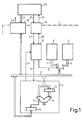
- a microcontroller 1 is indicated in FIG. 1, which is constructed as a monolithically integrated circuit and is connected to a test arrangement 22.
- FIG. 1 A microcontroller 1 is indicated in FIG. 1, which is constructed as a monolithically integrated circuit and is connected to a test arrangement 22.
- the microcontroller 1 only the elements important for the following explanation are shown, while other elements are omitted for the sake of clarity.
- An essential element of the microcontroller 1 is the processor 2, also referred to as the CPU, which contains a number of circuits, of which only the circuits important for the following explanation are also shown here.
- This is the arithmetic-logic processing unit 12, which is generally referred to as ALU.
- a register 14 is specified, the output of which is connected to the one data input of the ALU, while the other input of the ALU 12 and the input of the register are connected to a schematically represented internal bus 3.
- a program memory 4 which contains the program to be executed by the microcontroller in normal operation and which is designed as a read-only memory (ROM), and a further read-only memory 6 which contains the test program.
- the output 5 of the ROM 4 and the output 7 of the test program memory 6 can optionally be connected to the internal bus 3 via a changeover switch 8.
- the addressing of the memories 4 and 6 is not shown separately and is carried out in the usual way by the processor 2 via address lines in the bus 3. If the test program works without loops and jumps, however, the test program memory 6 could also be by one separate address generator, for example a counter, can be controlled.
- a test control circuit 10 is present in any case for testing the integrated circuit 1, regardless of the described test of the content of the ROM 4.
- the microcontroller 1 is connected to a test arrangement 22 for testing via the input / output circuits 18 and 20 which are present anyway.
- the input-output circuits 18 and 20 contain driver circuits for outgoing lines and receive circuits for incoming lines, which are at least partially controllable or switchable. This applies in particular to the input / output circuits 18, via which data words can be exchanged with externally connected devices, in this case with the test arrangement 22.
- the outgoing data lines are often provided with a register in the arrangement 18, so that this data only has to be generated for a short time by the processor 2 and is available to the outside for a long time.
- the test arrangement 22 now sends a signal for setting the test mode via the line 27, which can actually also comprise several lines, which signal is sent via the input / output circuit 20 and the line 21 to the test control circuit 10 is fed.
- both the test arrangement 22 and the microcontroller 1 were set to an initial position via a reset signal (not shown).
- the test control circuit 10 now brings the changeover switch 8 into the position shown via the line 11 and thus feeds the first test command from the test program memory 6 via the bus 3 to the processor 2, where it is stored, for example, in a command register (not shown). This may be followed by further commands which place the processor 2 in a desired state.
- the processor 2 can also be set to the test mode via a connection 9.
- the test control circuit 10 then briefly switches the changeover switch 8 and feeds the first data word from the ROM 4 via the bus 3 to the processor 2, where it is temporarily stored in the register 14 and is present at an input of the ALU 12. Then the switch 8 is switched back to the position shown and a data word generated by the test arrangement 22 on the output line 23, which corresponds to the first correct data word in the ROM 4, via the input-output circuit 18 and the bus 3 to the other input of the ALU 12 supplied, and then the two data words are compared, for example by setting the ALU to subtraction or to a logical comparison function, if this is provided.
- Line 17 merely indicates whether equality or inequality has been determined. In the latter case, i.e. the first word in the ROM 4 does not match the specified content, the corresponding signal is written into the register 16 on the line 17.
- the address for the ROM 4 is increased by 1, and also over the line 13 of the test control circuit 10 is supplied with a signal for the end of a test step, and the test control circuit 10 then sends out via line 19 a synchronizing signal which is supplied to the test arrangement 22 via the input / output circuit 20 and line 29 and there the next comparison value on line-23. Furthermore, the switch 8 is switched back to the position shown via line 11 and the next test step is carried out in the same way. In this way, the content of the ROM 4 is successively compared with corresponding comparison values of the test arrangement 22. If several error signals are generated on line 17, the content of register 16 as a binary number can also be increased by one step by means of appropriate control by CPU 2.
- the test control circuit 10 ends the test and finally switches the switch 8 to the position not shown, and also the content of the register 16, the output of which can be connected in the usual way to the bus 3, output via the input-output circuit 18 at an output 25.
- This is usually a data word in which e.g. the values of certain data bits indicate whether an error signal has occurred during the test or not.
- block 30 the entire arrangement, ie the microcontroller and the test arrangement, is reset to a defined initial state.
- a counter in the test arrangement 22, which successively addresses the test data is set to the initial position, and in block 32 the address of the ROM is set to the initial address.
- the ALU or its associated accumulator register is set to zero in block 33.
- a signal is generated via the input / output circuit, which causes the test arrangement to supply the next test data to the microcontroller.
- the memory location addressed by the processor is read out in the ROM and fed to the processor, and in block 36 the test data generated by the test arrangement is read.
- the address for the ROM is incrementally increased by 1.
- block 40 it is now checked whether the data read from the ROM (block 35) match the data supplied by the test arrangement 22 (block 36). If this is not the case, an error register is set in block 44 or an error counter is counted on and then proceeded to block 41, while if the two data match, the process goes directly to block 41, in which the signal at the output of the microcontroller, the data requests from the test arrangement 22, is reset. Finally, it is checked in block 42 whether the highest address of the ROM has been read out last, i.e. because of block 37 whether the next address provided by the processor is greater than the highest address of the ROM. If this is not the case, the process returns to block 33 and the process is repeated again.
- the content of the error register or error counter can also be given to the outside after block 42, since its content immediately indicates whether an error has occurred.
Landscapes
- Microcomputers (AREA)
- For Increasing The Reliability Of Semiconductor Memories (AREA)
- Read Only Memory (AREA)
- Test And Diagnosis Of Digital Computers (AREA)
- Techniques For Improving Reliability Of Storages (AREA)
Claims (7)
- Procédé de contrôle du contenu d'une mémoire morte (4) dans un circuit intégré (1), qui contient en outre un processeur (2) commandé par le contenu de la mémoire morte (4) comportant une unité de calcul (12) et une unité de mémoire (16), le processeur (2) étant connecté aux connexions externes (23, 29) du circuit intégré (1) et pouvant être commuté dans un mode de contrôle dans lequel le contenu de la mémoire morte (4) à l'intérieur du circuit intégré (1) est comparé à des données de contrôle acheminées de l'extérieur et, en cas de non-coïncidence, un message d'erreur est produit, caractérisé en ce qu'il est prévu un programme de contrôle mémorisé dans une mémoire de programme de contrôle (6) qui est activée dans le mode de contrôle du processeur (2) et, lors de son exécution, le contenu de la mémoire morte (4) est extrait par le processeur (2) successivement et est chaque fois acheminé à l'unité de calcul (12) conjointement avec les données de contrôle correspondantes acheminées de l'extérieur, pour comparaison et un message d'erreur qui apparaît est mémorisé dans le registre de mémoire (16), ce message d'erreur n'étant délivré qu'à la fin du programme du contrôle via une connexion (25) jouant le rôle de connexion de données au cours d'un fonctionnement normal du processeur (2).
- Procédé selon la revendication 1, caractérisé en ce que chaque message d'erreur apparaissant fait l'objet d'un stockage intermédiaire et, à la fin du programme de contrôle, une indication du nombre de messages d'erreur est délivrée à l'extérieur.
- Agencement pour l'exécution du procédé selon la revendication 1 ou 2 avec un circuit intégré (1) qui contient un processeur (2) comportant une unité de calcul (12) et au moins un registre de mémoire (16) et une mémoire morte (4) ainsi qu'un certain nombre de connexions externes (23-29), dont au moins une est connectée à un dispositif de contrôle (22) fournissant des données de contrôle, caractérisé en ce que, dans le circuit intégré (1), il est prévu une mémoire de programme de contrôle (6) pour recevoir des instructions de commande d'un programme de contrôle et le processeur (2), après réglage sur le mode de contrôle, extrait les instructions de commande de la mémoire de programme de contrôle (6) et, sous la commande de ces instructions de commande, extrait les données de la mémoire morte (4) successivement et, conjointement avec les données de contrôle acheminées, les envoie à l'unité de calcul (12) pour comparaison et, dans le cas d'un signal de commande de l'unité de calcul (12) indiquant l'inégalité des données acheminées, modifie le contenu du registre de stockage (16) par rapport à un état de départ prédéterminé et envoie, à la fin du programme de contrôle, le contenu du registre de stockage (16) à une connexion (25) jouant le rôle de sortie de données au cours de l'exploitation normale du circuit intégré (1).
- Agencement selon la revendication 3, caractérisé en ce que le processeur (2) augmente le contenu du registre de stockage (16) d'une unité sous la forme d'un nombre binaire à chaque apparition d'un signal de commande de l'unité de calcul (12).
- Agencement selon la revendication 3 ou 4, caractérisé en ce que la mémoire morte (4) et la mémoire de programme de contrôle (6) sont connectées au processeur (2) via un commutateur (8) réglé en fonction du mode de contrôle et du déroulement du contrôle.
- Agencement selon l'une quelconque des revendications 3 à 5, caractérisé en ce que la mémoire de programme de contrôle (6) est une mémoire morte.
- Agencement selon l'une quelconque des revendications 3 à 6, caractérisé en ce que le contenu de la mémoire de programme de contrôle (6) est accessible de l'extérieur du circuit intégré (1).
Applications Claiming Priority (2)
| Application Number | Priority Date | Filing Date | Title |
|---|---|---|---|
| DE3820728A DE3820728A1 (de) | 1988-06-18 | 1988-06-18 | Verfahren zum pruefen eines festwertspeichers und anordnung zur durchfuehrung des verfahrens |
| DE3820728 | 1988-06-18 |
Publications (3)
| Publication Number | Publication Date |
|---|---|
| EP0347970A2 EP0347970A2 (fr) | 1989-12-27 |
| EP0347970A3 EP0347970A3 (fr) | 1991-04-03 |
| EP0347970B1 true EP0347970B1 (fr) | 1994-02-16 |
Family
ID=6356809
Family Applications (1)
| Application Number | Title | Priority Date | Filing Date |
|---|---|---|---|
| EP89201501A Expired - Lifetime EP0347970B1 (fr) | 1988-06-18 | 1989-06-12 | Procédé de test de mémoire morte et dispositif de mise en application dudit procédé |
Country Status (4)
| Country | Link |
|---|---|
| US (1) | US5048019A (fr) |
| EP (1) | EP0347970B1 (fr) |
| JP (1) | JP2866896B2 (fr) |
| DE (2) | DE3820728A1 (fr) |
Families Citing this family (10)
| Publication number | Priority date | Publication date | Assignee | Title |
|---|---|---|---|---|
| JPH069000B2 (ja) * | 1981-08-27 | 1994-02-02 | キヤノン株式会社 | 音声情報処理方法 |
| JPH0821028B2 (ja) * | 1986-04-23 | 1996-03-04 | 株式会社日立製作所 | デ−タ処理装置 |
| ATE133512T1 (de) * | 1990-05-31 | 1996-02-15 | Siemens Ag | Integrierter halbleiterspeicher |
| JP2806026B2 (ja) * | 1990-09-26 | 1998-09-30 | ヤマハ株式会社 | メモリテスト回路 |
| US5313618A (en) * | 1992-09-03 | 1994-05-17 | Metalink Corp. | Shared bus in-circuit emulator system and method |
| US5428770A (en) * | 1993-08-31 | 1995-06-27 | Motorola, Inc. | Single-chip microcontroller with efficient peripheral testability |
| JP2004152027A (ja) * | 2002-10-30 | 2004-05-27 | Matsushita Electric Ind Co Ltd | 不揮発性メモリ内蔵マイクロコンピュータチップ、及びその検査方法 |
| DE10327284B4 (de) * | 2003-06-17 | 2005-11-03 | Infineon Technologies Ag | Prüflesevorrichtung für Speicher |
| JP4045262B2 (ja) * | 2004-07-02 | 2008-02-13 | 沖電気工業株式会社 | Romテスト方法及びromテスト回路 |
| US10249380B2 (en) * | 2017-01-27 | 2019-04-02 | Qualcomm Incorporated | Embedded memory testing with storage borrowing |
Family Cites Families (10)
| Publication number | Priority date | Publication date | Assignee | Title |
|---|---|---|---|---|
| JPS55128641A (en) * | 1979-03-23 | 1980-10-04 | Nissan Motor Co Ltd | Controlling system for vehicle |
| US4334307A (en) * | 1979-12-28 | 1982-06-08 | Honeywell Information Systems Inc. | Data processing system with self testing and configuration mapping capability |
| US4455654B1 (en) * | 1981-06-05 | 1991-04-30 | Test apparatus for electronic assemblies employing a microprocessor | |
| FR2531230A1 (fr) * | 1982-07-27 | 1984-02-03 | Rank Xerox Sa | Ensemble destine au test automatique centralise de circuits imprimes et procede de test de circuits a microprocesseur faisant application de cet ensemble |
| US4691316A (en) * | 1985-02-14 | 1987-09-01 | Support Technologies, Inc. | ROM emulator for diagnostic tester |
| JPS6267800A (ja) * | 1985-09-20 | 1987-03-27 | Hitachi Ltd | 半導体集積回路装置 |
| JPS6352251A (ja) * | 1986-08-22 | 1988-03-05 | Hitachi Ltd | 半導体集積回路 |
| JPS63108600A (ja) * | 1986-10-27 | 1988-05-13 | Nec Corp | 半導体装置 |
| US4868822A (en) * | 1988-02-19 | 1989-09-19 | John Fluke Mfg. Co., Inc. | Memory emulation method and system for testing and troubleshooting microprocessor-based electronic systems |
| US4933941A (en) * | 1988-06-07 | 1990-06-12 | Honeywell Bull Inc. | Apparatus and method for testing the operation of a central processing unit of a data processing system |
-
1988
- 1988-06-18 DE DE3820728A patent/DE3820728A1/de not_active Withdrawn
-
1989
- 1989-06-12 DE DE89201501T patent/DE58906967D1/de not_active Expired - Fee Related
- 1989-06-12 EP EP89201501A patent/EP0347970B1/fr not_active Expired - Lifetime
- 1989-06-15 US US07/366,571 patent/US5048019A/en not_active Expired - Lifetime
- 1989-06-16 JP JP15247789A patent/JP2866896B2/ja not_active Expired - Fee Related
Also Published As
| Publication number | Publication date |
|---|---|
| DE58906967D1 (de) | 1994-03-24 |
| JP2866896B2 (ja) | 1999-03-08 |
| EP0347970A3 (fr) | 1991-04-03 |
| JPH0237600A (ja) | 1990-02-07 |
| US5048019A (en) | 1991-09-10 |
| EP0347970A2 (fr) | 1989-12-27 |
| DE3820728A1 (de) | 1989-12-21 |
Similar Documents
| Publication | Publication Date | Title |
|---|---|---|
| DE3210816C2 (fr) | ||
| DE69906156T2 (de) | Mikroprozessorvorrichtung mit programmierbaren wartezuständen | |
| DE68925466T2 (de) | Zeitgeberschaltung | |
| DE69331292T2 (de) | Elektronisches Gerät und Verfahren zur festen Informationsmodifikation | |
| DE2619159A1 (de) | Fehlererkennungs- und korrektureinrichtung | |
| DE69120765T2 (de) | Verfahren zum Datentransfer zu oder von Vorrichtungen über eine Boundary-Scan-Test-Schnittstelle | |
| DE3685711T2 (de) | Anordnung zur simulation von rechnerfunktionen von grossrechenanlagen. | |
| DE1901228B2 (de) | Datenverarbeitungsanlage mit einrichtungen zur wiederholung von operationen beim auftreten eines fehlers | |
| DE2753062A1 (de) | Einrichtung zur durchfuehrung programmierter befehle | |
| DE2407241A1 (de) | Verfahren und anordnung zur erhoehung der verfuegbarkeit eines digitalrechners | |
| EP0347970B1 (fr) | Procédé de test de mémoire morte et dispositif de mise en application dudit procédé | |
| DE3751108T2 (de) | Mikroprozessor mit der Fähigkeit, an einen Koprozessor geschaltet zu werden. | |
| DE3507584C2 (fr) | ||
| EP2110995A1 (fr) | Dispositif de transmission des données | |
| DE3317593C2 (de) | Prüfsystem-Speicherarchitektur | |
| DE1185404B (de) | Fehlerermittlungsanlage | |
| DE2927481A1 (de) | Datenverarbeitungsvorrichtung | |
| DE2245284A1 (de) | Datenverarbeitungsanlage | |
| DE3210616A1 (de) | Rechner | |
| DE69122001T2 (de) | Integrierte Schaltung mit einer Standardzelle, einer Anwendungszelle und einer Prüfzelle | |
| EP1278120A1 (fr) | Contrôleur et procédé de commander un CPU pour adressage de mémoire | |
| DE2106731A1 (de) | Diagnoseeinrichtung fur elektronische Datenverarbeitungsanlagen | |
| DE3009121C2 (de) | Mikroprogramm-Steuereinrichtung | |
| DE102004006767A1 (de) | Verfahren und Vorrichtung zum Transport von Datenabschnitten mittels eines DMA-Controllers | |
| DE69431338T2 (de) | Datenverarbeitungssystem mit Busbreite-Wechselfunktion |
Legal Events
| Date | Code | Title | Description |
|---|---|---|---|
| PUAI | Public reference made under article 153(3) epc to a published international application that has entered the european phase |
Free format text: ORIGINAL CODE: 0009012 |
|
| AK | Designated contracting states |
Kind code of ref document: A2 Designated state(s): DE FR GB |
|
| PUAL | Search report despatched |
Free format text: ORIGINAL CODE: 0009013 |
|
| AK | Designated contracting states |
Kind code of ref document: A3 Designated state(s): DE FR GB |
|
| 17P | Request for examination filed |
Effective date: 19910930 |
|
| 17Q | First examination report despatched |
Effective date: 19930511 |
|
| GRAA | (expected) grant |
Free format text: ORIGINAL CODE: 0009210 |
|
| AK | Designated contracting states |
Kind code of ref document: B1 Designated state(s): DE FR GB |
|
| REF | Corresponds to: |
Ref document number: 58906967 Country of ref document: DE Date of ref document: 19940324 |
|
| GBT | Gb: translation of ep patent filed (gb section 77(6)(a)/1977) |
Effective date: 19940504 |
|
| ET | Fr: translation filed | ||
| PLBE | No opposition filed within time limit |
Free format text: ORIGINAL CODE: 0009261 |
|
| STAA | Information on the status of an ep patent application or granted ep patent |
Free format text: STATUS: NO OPPOSITION FILED WITHIN TIME LIMIT |
|
| 26N | No opposition filed | ||
| REG | Reference to a national code |
Ref country code: FR Ref legal event code: CD |
|
| REG | Reference to a national code |
Ref country code: FR Ref legal event code: CD |
|
| REG | Reference to a national code |
Ref country code: GB Ref legal event code: IF02 |
|
| PGFP | Annual fee paid to national office [announced via postgrant information from national office to epo] |
Ref country code: GB Payment date: 20050628 Year of fee payment: 17 Ref country code: FR Payment date: 20050628 Year of fee payment: 17 |
|
| PGFP | Annual fee paid to national office [announced via postgrant information from national office to epo] |
Ref country code: DE Payment date: 20050816 Year of fee payment: 17 |
|
| PG25 | Lapsed in a contracting state [announced via postgrant information from national office to epo] |
Ref country code: GB Free format text: LAPSE BECAUSE OF NON-PAYMENT OF DUE FEES Effective date: 20060612 |
|
| PG25 | Lapsed in a contracting state [announced via postgrant information from national office to epo] |
Ref country code: DE Free format text: LAPSE BECAUSE OF NON-PAYMENT OF DUE FEES Effective date: 20070103 |
|
| GBPC | Gb: european patent ceased through non-payment of renewal fee |
Effective date: 20060612 |
|
| REG | Reference to a national code |
Ref country code: FR Ref legal event code: ST Effective date: 20070228 |
|
| PG25 | Lapsed in a contracting state [announced via postgrant information from national office to epo] |
Ref country code: FR Free format text: LAPSE BECAUSE OF NON-PAYMENT OF DUE FEES Effective date: 20060630 |