EP0342695A2 - Halbleitervorrichtung - Google Patents
Halbleitervorrichtung Download PDFInfo
- Publication number
- EP0342695A2 EP0342695A2 EP89109046A EP89109046A EP0342695A2 EP 0342695 A2 EP0342695 A2 EP 0342695A2 EP 89109046 A EP89109046 A EP 89109046A EP 89109046 A EP89109046 A EP 89109046A EP 0342695 A2 EP0342695 A2 EP 0342695A2
- Authority
- EP
- European Patent Office
- Prior art keywords
- region
- emitter
- transistor
- base region
- another
- Prior art date
- Legal status (The legal status is an assumption and is not a legal conclusion. Google has not performed a legal analysis and makes no representation as to the accuracy of the status listed.)
- Granted
Links
Images


Classifications
-
- H—ELECTRICITY
- H10—SEMICONDUCTOR DEVICES; ELECTRIC SOLID-STATE DEVICES NOT OTHERWISE PROVIDED FOR
- H10D—INORGANIC ELECTRIC SEMICONDUCTOR DEVICES
- H10D84/00—Integrated devices formed in or on semiconductor substrates that comprise only semiconducting layers, e.g. on Si wafers or on GaAs-on-Si wafers
- H10D84/60—Integrated devices formed in or on semiconductor substrates that comprise only semiconducting layers, e.g. on Si wafers or on GaAs-on-Si wafers characterised by the integration of at least one component covered by groups H10D10/00 or H10D18/00, e.g. integration of BJTs
- H10D84/641—Combinations of only vertical BJTs
- H10D84/642—Combinations of non-inverted vertical BJTs of the same conductivity type having different characteristics, e.g. Darlington transistors
-
- H—ELECTRICITY
- H10—SEMICONDUCTOR DEVICES; ELECTRIC SOLID-STATE DEVICES NOT OTHERWISE PROVIDED FOR
- H10D—INORGANIC ELECTRIC SEMICONDUCTOR DEVICES
- H10D84/00—Integrated devices formed in or on semiconductor substrates that comprise only semiconducting layers, e.g. on Si wafers or on GaAs-on-Si wafers
- H10D84/01—Manufacture or treatment
- H10D84/0112—Integrating together multiple components covered by H10D8/00, H10D10/00 or H10D18/00, e.g. integrating multiple BJTs
-
- H—ELECTRICITY
- H10—SEMICONDUCTOR DEVICES; ELECTRIC SOLID-STATE DEVICES NOT OTHERWISE PROVIDED FOR
- H10D—INORGANIC ELECTRIC SEMICONDUCTOR DEVICES
- H10D84/00—Integrated devices formed in or on semiconductor substrates that comprise only semiconducting layers, e.g. on Si wafers or on GaAs-on-Si wafers
- H10D84/01—Manufacture or treatment
- H10D84/02—Manufacture or treatment characterised by using material-based technologies
- H10D84/03—Manufacture or treatment characterised by using material-based technologies using Group IV technology, e.g. silicon technology or silicon-carbide [SiC] technology
- H10D84/038—Manufacture or treatment characterised by using material-based technologies using Group IV technology, e.g. silicon technology or silicon-carbide [SiC] technology using silicon technology, e.g. SiGe
Definitions
- the present invention relates to a semiconductor device such as an IC, LSI, and VLSI, comprising a high-speed transistor and a high-current (or output) transistor formed in a common substrate.
- the semiconductor device generally comprises high-speed bipolar transistors (or field-effect transistors: FETs) for an arithmetic unit, a logic circuit, memory elements, and the like, and high-current bipolar transistors (or FET's) for an output circuit.
- FETs field-effect transistors
- FET's high-current bipolar transistors
- a suitable balance of the static common-emitter current gains h FE of both transistors should be maintained, to ensure a stable operation and enable a simple circuit design for the device.
- a suitable h FE balance is that where the h FE of the high-current bipolar transistor is within ⁇ 30% of that of the high-speed bipolar transistor.
- both bipolar transistors have the same emitter width of several micrometers (i.e., more than 1 ⁇ m) in view of the h FE balance.
- the shallow junction structure is formed by a thermal diffusion of impurities into a silicon substrate (particularly, a silicon epitaxial layer corresponding to a collector region) from a polycrystalline silicon layer doped with the impurities by an ion-implantation process.
- the emitter width is made narrower (less than 1 ⁇ m) for a higher operation speed, shallower shallow junction, lower power consumption, and in view of device miniaturization.
- the high-speed bipolar transistor can operate at 0.1 mA.
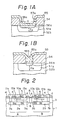
- the emitter width should be wider than that of the high-speed bipolar transistor, but a simultaneous fabrication of the bipolar transistor with a narrow emitter width (Fig. 1B) and the bipolar transistor with a wide emitter width (Fig. 1A) leads to an h FE unbalance.
- base regions 51a and 51b having the same depth are simultaneously formed in collector regions 52a and 52b, which are portions of an epitaxial Si layer on an Si substrate (not shown).
- a wide emitter window 53a having an emitter width X of, e.g., 1.5 ⁇ m, and a narrow emitter window 54b having an emitter width Y of, e.g., 0.5 ⁇ m, are opened in an insulating (SiO2) layer 54 covering the epitaxial layer, and when a polycrystalline silicon layer 55 having a thickness of, e.g., 100 nm, is deposited over the whole surface by a chemical vapor deposition (CVD) process, a portion 55b of the layer 55 filling the window 53b is thicker than a portion 55a filling the window 53a.
- SiO2 insulating
- the polycrystalline silicon layer 55 is then doped with impurities by an ion-implantation process at the projected range R p of, e.g., 50 nm.
- the device is subjected to a heat-treatment at 950°C for 30 minutes, so that emitter regions 56a and 56b are formed in the base region 51a and 52b, respectively.
- the emitter region 56a has a depth of, e.g., 150 nm
- the emitter region 56b has a depth of, e.g., 100 nm.
- the emitter region 56b is shallower (thinner) than the emitter region 56a, because the filling portion 55b includes an undoped portion thicker than that included in the filling portion 55a, and as a result, an active base region thickness Za of the wide emitter is smaller than the Zb of the narrow emitter.
- the h FE is in inverse proportion to the amount of impurities in the active base region, and therefore, as the thickness of the active base becomes thinner, the h FE becomes larger and is not suitably balanced.
- a multi-emitter structure increasing the number of the emitter regions, or an elongation of an emitter length, may be adopted, but this leads to an enlargement of the transistor size, which does not allow a miniaturization of the device and prevents an increase of the degree of integration.
- An object of the present invention is to provide a semiconductor device comprising shallow junction type bipolar transistors, the emitter regions of which have different submicron widths, while maintaining a suitable h FE balance.
- Another object of the present invention is to provide a semiconductor device comprising a high-speed transistor and a high-current transistor, the device miniaturization and integration degree of which are improved.
- a further object of the present invention is to provide a semiconductor device comprising a shallow junction type bipolar transistor and a junction field-effect transistor (JFET) having an impurity-containing layer serving as an impurity diffusion source for a gate region.
- JFET junction field-effect transistor
- Still another object of the present invention is to provide a semiconductor device comprising a high-speed JFET and a high-current JFET, the gate regions of which are formed by a thermal diffusion of impurities from an impurity-containing layer on both transistors.
- a semiconductor device comprising a first (high-current) transistor having a wide emitter width and a second (high-speed) transistor having a narrow emitter width, both transistors being formed in a common semiconductor substrate, and according to a first embodiment of the present invention, a first base region of the first transistor is thicker than a second base region of the second transistor, so that a suitable h FE balance is maintained.
- the first base region is made deeper than the second base region by controlling the ion-implantation energy, with the result that a first active base region thickness under the first emitter region is similar or equal to a second active base region under the second emitter region.
- the wide emitter width is from 0.4 to 4.0 ⁇ m (in particular, 0.45 to 1.0 ⁇ m) and the narrow emitter width is from 0.1 to 0.75 ⁇ m (in particular, 0.2 to 0.4 ⁇ m).
- the semiconductor device according to a second embodiment of the present invention, wherein a first base region of the first transistor has a higher impurity concentration than that of a second base region of the second transistor and has the same depth as that of the second base region, so that a suitable h FE balance is maintained.
- the impurity concentration of the first base region corresponds to a dose of from 3 to 10 (in particular, 4 to 7) x 1013cm ⁇ 2 and that of the second base region corresponds to a dose of from 1 to 8 (in particular, 3 to 6) x 1013cm ⁇ 2.
- the impurity amount of the first active base region is similar or equal to that of the second active base region.
- the base region thickness control and the base region impurity concentration control according to the present invention can be applied to a channel region (or channel regions) of a JFET (or JFETs) included in a semiconductor device comprising a first (high-current transistor and a second (high-speed) transistor.
- a semiconductor device comprising a high-current (output) bipolar transistor A and a high-speed bipolar transistor B according to a first embodiment of the present invention is now explained.
- both of the npn-type transistors A and B are formed in a common semiconductor substrate consisting of a p-type semiconductor (Si) substrate (wafer) 1 and an n-type semiconductor (epitaxial Si) layer 3 having a resistivity of 0.5 ⁇ cm and a thickness of 1.6 ⁇ m, and n+-type buried layers 2a and 2b having a resistivity of 20 ⁇ / and a thickness of 3 ⁇ m are separately formed between the substrate 1 and the epitaxial layer 3.
- the epitaxial layer 3 is covered with a relatively thick insulating layer (field SiO2 layer) 4 having a thickness of 600 nm and a thin insulating layer 5 having a thickness of 50 nm, and is divided into collector regions 3a and 3b by an isolation region 6 composed of a p+-type impurity doped region (or insulator).
- the collector contact (n+-type) regions 7a and 7b extend from the surface of the collector regions 3a and 3b to the buried layers 2a and 2b, respectively.
- p+-type base regions 9a and 9b are formed in the collector regions 3a and 3b, respectively, and N+-type emitter regions 8a and 8b are formed in the base regions 9a and 9b, and covered with impurity-containing layers 10a and 10b of, e.g., polycrystalline silicon, containing donor impurities and having a thickness of 100 nm.
- Electrodes are formed on the collector contact regions 7a, 7b, the impurity-containing layers 10a, 10b and the base regions 9a, 9b, respectively, and accordingly, the high-current bipolar transistor A is composed of the collector region 3a, base region 9a, emitter region 8a, and electrodes 11a, 12a and 13a, and the high-speed bipolar transistor B is composed of the collector region 3b, base region 9b, emitter region 8b, and electrodes 11b, 12b and 13b.
- the base region 9a has a depth of from 0.45 to 0.55 ⁇ m and the base region 9b has a depth of from 0.3 to 0.4 ⁇ m, and thus is shallower than the region 9a.
- the high-current transistor A has a wide emitter width of 2.0 ⁇ m, and accordingly, the emitter region 8a has a depth of 0.25 ⁇ m, and the high-speed transistor B has a narrow emitter width on the order of submicrons (0.6 ⁇ m), and thus the emitter region 8b has a depth of 0.15 ⁇ m, which is less than that of the region 8a.
- the static common-emitter current gains h FE of both transistors A and B can be made roughly equivalent (e.g., an h FE difference between the high-current transistor A and high-speed transistor B can be kept to within ⁇ 30% of the h FE of the high-speed transistor B). Therefore, while maintaining the h FE balance between the high-current transistor A and high-speed transistor B, the emitter width of the high-current transistor A can be suitably expanded, so that the transistor A operates at an operating current of, e.g., 30 mA.
- the high-current power transistor A occupies about half (50%) of the space required by a conventional power transistor having a multi-emitter structure, and this reduction of size of the high-current bipolar transistors contributes to a miniaturization of, and an increase of the integration degree of, an IC device.
- the semiconductor device shown in Fig. 2 is produced as follows and as shown in Figs. 3A to 3C.
- donor impurities e.g., Sb
- the n-type Si layer 3 having a thickness of 600 nm is epitaxially grown on the Si substrate 1 to form the n+-type buried layers 2a and 2b having a thickness of 3 ⁇ m and a resistivity of 20 ⁇ / ⁇ .
- the Si epitaxial layer 3 is thermally and selectively oxidized to the field SiO2 layer 4 having a thickness of 600 nm, by the LOCOS process, donor impurities are selectively introduced into the Si epitaxial layer 3 and acceptor impurities are selectively introduced into the layer 3, and then the Si epitaxial layer 3 is thermally oxidized so that a thin SiO2 layer 5 having a thickness of 50 nm is formed, and simultaneously, an annealing is carried out to form the collector regions 7a and 7b reaching the buried layers 2a and 2b and the p+-type isolation region 6 reaching the Si substrate 1, to divide the Si epitaxial layer into the collector regions 3a and 3b.
- acceptor impurities e.g., boron ions
- acceptor impurities e.g., boron ions
- the same acceptor impurities are introduced into the collector region 3b through the SiO2 layer 5 by an ion-implantation process at an energy of 35 keV and a dose of 5 x 1013 cm ⁇ 2. Therefore, although the doses are the same, the implantation energies are different.
- an annealing (heat-treatment) after ion-implantation is carried out at 900°C for 30 minutes, so that the base region 9a having a depth of from 0.45 to 0.5 ⁇ m and the base region 9b having a depth of from 0.3 to 0.4 ⁇ m are formed in the collector regions 3a and 3b, respectively. Therefore, the base region 9a is thicker than the base region 9b.
- the insulating layer (SiO2 layer) 5 is selectively etched by a conventional lithographic and etching process to form emitter windows 14a and 14b in which the base regions 9a and 9b are exposed, respectively.
- the emitter window 14a has a width of 2.0 ⁇ m and the emitter window 14b for the high-speed transistor has a width of 0.6 ⁇ m.
- a SiO2 layer (not shown) may be additionally deposited over the whole surface by a CVD process.
- a reactive ion etching process is used as the etching process.
- a polycrystalline silicon layer having a thickness of 100 nm is deposited over the whole surface by a CVD process, so that the windows 14a and 14b are completely filled therewith, and donor impurities (e.g., arsenic ions) are introduced into the polycrystalline Si layer only by an ion-implantation process at an energy of 60 keV and a dose of 5 x 1015 cm ⁇ 2, to form the impurity-containing layer 10.
- donor impurities e.g., arsenic ions
- the device is subjected to a heat-treatment at 950°C for 30 minutes, and as a result, as shown in Fig.
- the emitter regions 8a and 8b are formed to depths of 0.25 ⁇ m and 0.15 ⁇ m, respectively.
- the impurity-containing layer 10 is selectively etched by a conventional process to leave the portions 10a and 10b of the layer 10 on the emitter regions 8a and 8b, and the thin SiO2 layer 5 is selectively etched to form contact windows for the collector contact regions 7a and 7b and the base regions 3a and 3b.
- a conductor layer is then deposited over the whole surface and is patterned (selectively etched) to form the electrodes 11a, 11b, 12a, 12b, 13a and 13b, whereby the semiconductor device shown in Fig. 2 is obtained.
- a semiconductor device comprising a high-current bipolar transistor A′ and a high-speed bipolar transistor B′ according to a second embodiment of the present invention is now explained.
- the reference numerals used in Figs. 2 and 3A to 3C are used in Figs. 4A to 4C, these reference numerals indicate the same portions as, or portions corresponding to, those used in Figs. 2 and 3A to 3C.
- both of the npn-type transistor A′ and B′ are formed in a common semiconductor substrate consisting of a p-type semiconductor Si wafer substrate 1 and n-type epitaxial Si layer 3.
- the n+-type buried layers 2a, 2b, the collector regions 3a and 3b, the n+-type collector contact regions 7a, 7b, the emitter regions 8a, 8b, the isolation region 6, the thick insulating (SiO2) layer 4, the thin insulating (SiO2) layer 5, the impurity-containing layer portions 10a, 10b, and the electrodes 11a, 11b, 12a, 12b, 13a, 13b are the same as those of the semiconductor device shown in Fig. 2.
- a p+-type base region 19a of the high-current transistor A′ and a p+-type base region 19b of the high-speed transistor B′ have the same depth of 0.15 ⁇ m, but the former region 19a has an impurity concentration (a dose of 8 x 1013 cm ⁇ 2) higher than that (a dose of 5 x 1013 cm ⁇ 2) of the latter region 19b.
- the base region 19a has a depth deeper than that of the base region 19b, a distance between the emitter-base junction face and the base collector junction face (i.e., an active base region thickness under the emitter region 8a) is smaller (an active base region thickness under the emitter region 8b.
- the impurity concentration of the base region 19a is higher than that of the base region 19b.
- the impurity amount of the active base region of the high-current transistor A′ can become, accordingly, almost equivalent to that of the active base region of the high-speed transistor B′.
- the static common-emitter current gains h FE of the transistors A′ and B′ can be made roughly equivalent, as obtained in the device shown in Fig. 2 of the first embodiment. Therefore, the device shown in Fig. 4C has the same advantages as those of the device of the first embodiment.
- the semiconductor device (shown in Fig. 4C) of the second embodiment of the present invention is produced as follows and as shown in Fig. 3A and Figs. 4A to 4C.
- the n+-type buried layers 2a, 2b, the n-type epitaxial Si layer 3 including the collector regions 3a, 3b, the thick SiO2 layer 4, the thin SiO2 layer 5, the p+-type isolation region 6, and the n+-type collector contact region are formed as explained in the first embodiment.
- the buried layers 2a and 2b have a thickness of 3 ⁇ m and a resistivity of 20 ⁇ / ⁇ , and the epitaxial Si layer has a thickness of 600 nm.
- acceptor impurities e.g., boron ions
- acceptor impurities e.g., boron ions
- the same acceptor impurities are then introduced into the collector region 3a only of the power transistor A′ at the same energy (35 keV) and a dose of 3 x 1013 cm ⁇ 2.
- the p+-type base regions 19a and 19b are formed and the former region 19a has an impurity concentration higher than that of the latter region 19b, but has the same depth as the latter region 19b. It is possible to form the base region 19a with boron ions at a dose of 8 x 1013 cm ⁇ 2 and to form the base region 19b with boron ions at a dose of 5 x 1013 cm ⁇ 2, by respective ion-implantation processes at a constant energy of 35 keV.
- the thin SiO2 layer 5 is selectively etched by a conventional lithographic and etching process to form emitter windows 14a and 14b, to expose portions of the base regions 19a and 19b, in a manner similar to that explained in the first embodiment. Then a polycrystalline silicon layer having a thickness of 100 nm is deposited over the whole surface by a CVD process, to fill the windows 14a and 14b, and donor impurities (e.g., arsenic ions) are introduced into the polycrystalline silicon layer 10 only by an ion-implantation process at an energy of 60 keV, and a dose of 5 x 1015 cm ⁇ 2, to form the impurity-containing layer 10.
- donor impurities e.g., arsenic ions
- the device with the arsenic-containing layer 10 is subjected to a heat-treatment at 950°C for 30 minutes, to form the emitter regions 8a and 8b in the base regions 19a and 19b, respectively.
- the emitter region 8a has a depth of 0.25 ⁇ m and the emitter region 8b has a depth of 0.15 ⁇ m.
- the impurity-containing layer 10 is selectively etched to leave the portions 10a and 10b on the emitter regions 8a and 8b, and the thin SiO2 layer 5 is selectively etched to form contact windows for the electrodes.
- a conductor layer is deposited over the whole surface and is patterned to form the emitter electrodes 11a, 11b, emitter electrodes 12a, 12b, and base electrodes 13a, 13b, and thus the semiconductor device is obtained.
- the emitter width of the high-current bipolar transistor is different from that of the high-speed bipolar transistor, the h FE valves of both transistors are kept at a similar or same level, and the high-current bipolar transistor size is reduced.
- a semiconductor device comprising a shallow junction type bipolar transistor (e.g., a high-speed bipolar transistor B the same as that shown in Fig. 2) and a junction field-effect transistor (JFET) C which serves as a high-current JFET and has a gate region formed by diffusing impurities from an impurity-containing layer.
- a shallow junction type bipolar transistor e.g., a high-speed bipolar transistor B the same as that shown in Fig. 2
- JFET junction field-effect transistor
- the p-channel JFET C comprises a p-type channel region 29, an n+-type top gate region 28, an n-type bottom gate region consisting of an n-type epitaxial layer region 3a, an n+-type buried layer 2a and an n+-type contact region 7a, and electrodes (a bottom gate electrode 21a, a top gate electrode 21b on an impurity-containing layer portion 10a, a sorce electrode 22 and a drain electrode 23).
- the gate electrodes 21a and 21b are electrically connected to each other, and the source and drain electrodes 22 and 23 are brought into contact with the channel region 29 and are arranged on both sides of the top gate electrode 21b.
- the channel region 29 is formed by an ion-implantation process at an energy of 160 keV and a dose of 5 x 1012cm ⁇ 2 of boron ions.
- the top gate region 28 corresponds to the wide emitter region 8a and is formed by a thermal diffusion of donor impurities (arsenic) from the impurity-containing layer portion 10a, as explained in the first embodiment, and thus the top gate region 28 has a depth of 0.25 ⁇ m.
- a semiconductor device comprising a JFET and a bipolar transistor has been proposed in, e.g., Japanese Unexamined Patent Publication (Kokai) No. 49-114882.
- an emitter region has a depth of 2.0 ⁇ m
- an active base region has a thickness of about 0.9 ⁇ m
- a top gate region has a depth of about 2.4 ⁇ m
- an active channel region has a thickness of about 0.6 ⁇ m.
- the bipolar transistor is not a shallow junction type and the semiconductor device does not reach a submicron miniaturization level.
- a semiconductor dervice comprises the high-current JFET C (the same as that shown in Fig. 5) and the high-speed JFET D.
- the reference numerals used in Figs. 2 and 5 are used in Fig. 6, those reference numerals indicate the same portions or the portions corresponding to those used in Fig. 2 and 5.
- the high-speed JFET D comprises a p-type channel region 39, an n+-type top gate region 38, an n-type bottom gate region consisting of an n-type epitaxial layer region 3b, an n+-type buried layer 2b, and an n+-type contact region 7b, and electrodes (a bottom gate electrode 31a, a top gate electrode 31b on an impurity-containing portion 10b, a source electrode 32 and a drain electrode 33).
- the gate electrodes 31a and 31b are electrically connected, and the source and drain electrodes 32 and 33 come into contact with the channel region 39 and are arranged on both sides of the top gate electrode 31b.
- the channel region 39 is formed by an ion-implantation process at an energy of 160 keV and a dose of x 1012cm ⁇ 2 of boron ions.
- the top gate region region 39 corresponds to the narrow emitter region 8b and is formed by a thermal diffusion of donor impurities (arsenic ) from the impurity-containing layer portion 10b, as explained in the first embodiment, and thus the top gate region 39 has a depth of 0.15 ⁇ m.
Landscapes
- Bipolar Transistors (AREA)
- Bipolar Integrated Circuits (AREA)
Applications Claiming Priority (2)
| Application Number | Priority Date | Filing Date | Title |
|---|---|---|---|
| JP124117/88 | 1988-05-20 | ||
| JP63124117A JPH0831473B2 (ja) | 1988-05-20 | 1988-05-20 | 半導体装置 |
Publications (3)
| Publication Number | Publication Date |
|---|---|
| EP0342695A2 true EP0342695A2 (de) | 1989-11-23 |
| EP0342695A3 EP0342695A3 (de) | 1990-11-22 |
| EP0342695B1 EP0342695B1 (de) | 1998-07-29 |
Family
ID=14877346
Family Applications (1)
| Application Number | Title | Priority Date | Filing Date |
|---|---|---|---|
| EP89109046A Expired - Lifetime EP0342695B1 (de) | 1988-05-20 | 1989-05-19 | Halbleitervorrichtung |
Country Status (5)
| Country | Link |
|---|---|
| US (1) | US5151765A (de) |
| EP (1) | EP0342695B1 (de) |
| JP (1) | JPH0831473B2 (de) |
| KR (1) | KR920008422B1 (de) |
| DE (1) | DE68928760T2 (de) |
Cited By (4)
| Publication number | Priority date | Publication date | Assignee | Title |
|---|---|---|---|---|
| US5648676A (en) * | 1990-09-10 | 1997-07-15 | Fujitsu Limited | Semiconductor device with protective element |
| NL1007898C2 (nl) * | 1996-12-26 | 2001-06-07 | Sony Corp | Werkwijze voor het vervaardigen van een halfgeleider-inrichting. |
| EP1229585A1 (de) * | 2001-02-02 | 2002-08-07 | Nec Corporation | Integrierter Schaltkreis mit bipolaren Transistoren unterschiedlicher Emitterweite |
| WO2019209870A1 (en) * | 2018-04-25 | 2019-10-31 | Qualcomm Incorporated | Heterojunction bipolar transistors and method of fabricating the same |
Families Citing this family (5)
| Publication number | Priority date | Publication date | Assignee | Title |
|---|---|---|---|---|
| JP2746499B2 (ja) * | 1992-05-15 | 1998-05-06 | 三菱電機株式会社 | 半導体装置及びその製造方法 |
| US5652153A (en) * | 1994-07-22 | 1997-07-29 | Harris Corporation | Method of making JFET structures for semiconductor devices with complementary bipolar transistors |
| JP3409548B2 (ja) * | 1995-12-12 | 2003-05-26 | ソニー株式会社 | 半導体装置の製造方法 |
| JPH09199513A (ja) * | 1996-01-19 | 1997-07-31 | Mitsubishi Electric Corp | バイポーラトランジスタおよび該バイポーラトランジスタを有する半導体装置 |
| US6555451B1 (en) * | 2001-09-28 | 2003-04-29 | The United States Of America As Represented By The Secretary Of The Navy | Method for making shallow diffusion junctions in semiconductors using elemental doping |
Family Cites Families (11)
| Publication number | Priority date | Publication date | Assignee | Title |
|---|---|---|---|---|
| JPS49114882A (de) * | 1973-02-28 | 1974-11-01 | ||
| JPS54113269A (en) * | 1978-02-24 | 1979-09-04 | Hitachi Ltd | Production of junction-type electronic field effect transistor |
| JPS55138267A (en) * | 1979-04-12 | 1980-10-28 | Matsushita Electric Ind Co Ltd | Manufacture of semiconductor integrated circuit containing resistance element |
| JPS57106160A (en) * | 1980-12-24 | 1982-07-01 | Hitachi Ltd | Semiconductor integrated circuit device and manufacture thereof |
| EP0093304B1 (de) * | 1982-04-19 | 1986-01-15 | Matsushita Electric Industrial Co., Ltd. | Integrierte Halbleiterschaltung und Verfahren zur Herstellung derselben |
| JPS5933860A (ja) * | 1982-08-19 | 1984-02-23 | Toshiba Corp | 半導体装置およびその製造方法 |
| JPS59182571A (ja) * | 1983-03-31 | 1984-10-17 | Fujitsu Ltd | 半導体装置 |
| JPH0682789B2 (ja) * | 1983-10-20 | 1994-10-19 | ローム株式会社 | 半導体装置の製造方法 |
| JPS6167271A (ja) * | 1984-09-10 | 1986-04-07 | Oki Electric Ind Co Ltd | 半導体装置の製造方法 |
| JPS63198367A (ja) * | 1987-02-13 | 1988-08-17 | Toshiba Corp | 半導体装置 |
| JPH01140761A (ja) * | 1987-11-27 | 1989-06-01 | Nec Corp | 半導体装置 |
-
1988
- 1988-05-20 JP JP63124117A patent/JPH0831473B2/ja not_active Expired - Fee Related
-
1989
- 1989-05-19 EP EP89109046A patent/EP0342695B1/de not_active Expired - Lifetime
- 1989-05-19 DE DE68928760T patent/DE68928760T2/de not_active Expired - Fee Related
- 1989-05-19 KR KR1019890006734A patent/KR920008422B1/ko not_active Expired
-
1991
- 1991-04-10 US US07/685,153 patent/US5151765A/en not_active Expired - Lifetime
Cited By (5)
| Publication number | Priority date | Publication date | Assignee | Title |
|---|---|---|---|---|
| US5648676A (en) * | 1990-09-10 | 1997-07-15 | Fujitsu Limited | Semiconductor device with protective element |
| US5670885A (en) * | 1990-09-10 | 1997-09-23 | Fujitsu Limited | Semiconductor device |
| NL1007898C2 (nl) * | 1996-12-26 | 2001-06-07 | Sony Corp | Werkwijze voor het vervaardigen van een halfgeleider-inrichting. |
| EP1229585A1 (de) * | 2001-02-02 | 2002-08-07 | Nec Corporation | Integrierter Schaltkreis mit bipolaren Transistoren unterschiedlicher Emitterweite |
| WO2019209870A1 (en) * | 2018-04-25 | 2019-10-31 | Qualcomm Incorporated | Heterojunction bipolar transistors and method of fabricating the same |
Also Published As
| Publication number | Publication date |
|---|---|
| EP0342695B1 (de) | 1998-07-29 |
| KR890017793A (ko) | 1989-12-18 |
| KR920008422B1 (ko) | 1992-09-28 |
| JPH0831473B2 (ja) | 1996-03-27 |
| EP0342695A3 (de) | 1990-11-22 |
| US5151765A (en) | 1992-09-29 |
| DE68928760D1 (de) | 1998-09-03 |
| JPH01293562A (ja) | 1989-11-27 |
| DE68928760T2 (de) | 1998-12-10 |
Similar Documents
| Publication | Publication Date | Title |
|---|---|---|
| US4637125A (en) | Method for making a semiconductor integrated device including bipolar transistor and CMOS transistor | |
| US3962717A (en) | Oxide isolated integrated injection logic with selective guard ring | |
| US4951102A (en) | Trench gate VCMOS | |
| US6930361B2 (en) | Semiconductor device realizing characteristics like a SOI MOSFET | |
| KR0126230B1 (ko) | 반도체 장치의 제조방법 | |
| US5137837A (en) | Radiation-hard, high-voltage semiconductive device structure fabricated on SOI substrate | |
| US5032529A (en) | Trench gate VCMOS method of manufacture | |
| US5354699A (en) | Method of manufacturing semiconductor integrated circuit device | |
| US4922315A (en) | Control gate lateral silicon-on-insulator bipolar transistor | |
| EP0341821A2 (de) | Verfahren zur Herstellung einer Halbleitervorrichtung | |
| JPH0521726A (ja) | BiCMOS装置及びその製造方法 | |
| US4985744A (en) | Method for forming a recessed contact bipolar transistor and field effect transistor | |
| US5075241A (en) | Method of forming a recessed contact bipolar transistor and field effect device | |
| US5047357A (en) | Method for forming emitters in a BiCMOS process | |
| US3993513A (en) | Combined method for fabricating oxide-isolated vertical bipolar transistors and complementary oxide-isolated lateral bipolar transistors and the resulting structures | |
| JPH04226064A (ja) | 半導体装置用の相互接続体及びその製造方法 | |
| EP0342695A2 (de) | Halbleitervorrichtung | |
| EP0239216A2 (de) | CMOS-compatibler bipolarer Transistor | |
| JPH0799259A (ja) | 縦型バイポーラトランジスタを有するBi−CMOS SOI構造及びその製造方法 | |
| JP2509690B2 (ja) | 半導体装置 | |
| US5057894A (en) | Semiconductor integrated circuit device | |
| US5150184A (en) | Method for forming emitters in a BiCMOS process | |
| JPS60163452A (ja) | バイポーラデバイスおよび電界効果デバイスを有する集積回路およびその製造方法 | |
| JPH0831542B2 (ja) | BiCMOS電界効果トランジスタの製造方法 | |
| US5506156A (en) | Method of fabricating bipolar transistor having high speed and MOS transistor having small size |
Legal Events
| Date | Code | Title | Description |
|---|---|---|---|
| PUAI | Public reference made under article 153(3) epc to a published international application that has entered the european phase |
Free format text: ORIGINAL CODE: 0009012 |
|
| AK | Designated contracting states |
Kind code of ref document: A2 Designated state(s): DE FR GB |
|
| PUAL | Search report despatched |
Free format text: ORIGINAL CODE: 0009013 |
|
| AK | Designated contracting states |
Kind code of ref document: A3 Designated state(s): DE FR GB |
|
| 17P | Request for examination filed |
Effective date: 19901219 |
|
| 17Q | First examination report despatched |
Effective date: 19921223 |
|
| GRAG | Despatch of communication of intention to grant |
Free format text: ORIGINAL CODE: EPIDOS AGRA |
|
| GRAG | Despatch of communication of intention to grant |
Free format text: ORIGINAL CODE: EPIDOS AGRA |
|
| GRAH | Despatch of communication of intention to grant a patent |
Free format text: ORIGINAL CODE: EPIDOS IGRA |
|
| RBV | Designated contracting states (corrected) |
Designated state(s): DE |
|
| GRAH | Despatch of communication of intention to grant a patent |
Free format text: ORIGINAL CODE: EPIDOS IGRA |
|
| GRAA | (expected) grant |
Free format text: ORIGINAL CODE: 0009210 |
|
| AK | Designated contracting states |
Kind code of ref document: B1 Designated state(s): DE |
|
| REF | Corresponds to: |
Ref document number: 68928760 Country of ref document: DE Date of ref document: 19980903 |
|
| PLBE | No opposition filed within time limit |
Free format text: ORIGINAL CODE: 0009261 |
|
| STAA | Information on the status of an ep patent application or granted ep patent |
Free format text: STATUS: NO OPPOSITION FILED WITHIN TIME LIMIT |
|
| 26N | No opposition filed | ||
| PGFP | Annual fee paid to national office [announced via postgrant information from national office to epo] |
Ref country code: DE Payment date: 20050512 Year of fee payment: 17 |
|
| PG25 | Lapsed in a contracting state [announced via postgrant information from national office to epo] |
Ref country code: DE Free format text: LAPSE BECAUSE OF NON-PAYMENT OF DUE FEES Effective date: 20061201 |