EP0341944A2 - Verfahren und Vorrichtungen zur Positionserfassung - Google Patents
Verfahren und Vorrichtungen zur Positionserfassung Download PDFInfo
- Publication number
- EP0341944A2 EP0341944A2 EP89304608A EP89304608A EP0341944A2 EP 0341944 A2 EP0341944 A2 EP 0341944A2 EP 89304608 A EP89304608 A EP 89304608A EP 89304608 A EP89304608 A EP 89304608A EP 0341944 A2 EP0341944 A2 EP 0341944A2
- Authority
- EP
- European Patent Office
- Prior art keywords
- article
- differences
- board
- registration
- surface characteristics
- Prior art date
- Legal status (The legal status is an assumption and is not a legal conclusion. Google has not performed a legal analysis and makes no representation as to the accuracy of the status listed.)
- Withdrawn
Links
Images
Classifications
-
- H—ELECTRICITY
- H05—ELECTRIC TECHNIQUES NOT OTHERWISE PROVIDED FOR
- H05K—PRINTED CIRCUITS; CASINGS OR CONSTRUCTIONAL DETAILS OF ELECTRIC APPARATUS; MANUFACTURE OF ASSEMBLAGES OF ELECTRICAL COMPONENTS
- H05K13/00—Apparatus or processes specially adapted for manufacturing or adjusting assemblages of electric components
- H05K13/08—Monitoring manufacture of assemblages
- H05K13/081—Integration of optical monitoring devices in assembly lines; Processes using optical monitoring devices specially adapted for controlling devices or machines in assembly lines
Definitions
- This invention concerns a method of registering an article in a predetermined disposition prior to manufacturing steps dependant upon the exactly known position of the article.
- One manufacturing procedure in which accurate article registration is necessary is the insertion or onsertion of components in predetermined locations of a printed circuit board (PCB).
- PCB's are produced by methods including photo-fabrication. To this end, they are provided with registration holes which mate with appropriate registration pins at the requisite stages of manufacture. Manufacturing tolerances are such that even when a PCB is mounted in engagement with the registration pins, it may not be sufficiently accurately aligned for subsequent placement of components thereon. This problem has been accentuated by the moves towards greater complexity of layout, increases in the number of components to be placed, size of the components and increases in packing density. A manufacturer must now either take greater care in reducing manufacturing tolerances (thus increasing costs) or alternatively must accept a higher rate of rejects (also increasing costs).
- a method of registration of an article of a series of articles whose surface characteristics must be accurately known for subsequent manufacturing steps comprising positioning a first article of the series on a comparator, comparing the surface characteristics of the article with a desired model, determining the differences between the surface characteristics of the article and the desired model, and storing the differences for subsequent use in manufacturing operations.
- the differences may be stored on a magnetic medium such as a floppy disc readable by subsequent apparatus, a manufacturing operation of which is dependant upon the surface characteristics of the article.
- the method of the invention may be effected as a first step and the differences may be fed in synchronism to subsequent production line stages whereat a manufacturing operation, requiring knowledge of the surface characteristics, is effected.
- a first article may be positioned on a registration plate which is adjustable to a best fit of the article and the model, the movement of the registration plate constituting a vector difference of a mean vector difference, which can be applied in a subsequent manufacturing stage.
- the registration plate may be held in its "best fit" position when a next article of the series of articles is positioned thereon and the surface characteristics of the next article compared with an up-dated model (to which the vector difference or the mean vector difference has been applied) and the registration plate again adjusted to a best fit of the article and up-dated model, the vector difference or the mean vector difference so determined being applied in the comparison of a next article of the series.
- the differences, or the mean difference which may be stored as vectors or a vector may be stored by means of a machine readable code applied to the article for reading by subsequent apparatus during manufacturing operations dependent upon the surface characteristics of the article.
- the article is a printed circuit board for the insertion or onsertion of components by subsequent gluing and/or placing machines
- the surface characteristics compared by the method of the invention are conveniently the individual component locations. The stored differences then permit a gluing and/or placing machine to carry out its operation with greater accuracy.
- the invention also provides article registration means comprising a registration plate whereon a first article of a series of articles may be mounted, means for viewing the surface characteristics of the article on a pixel-by-pixel basis and for comparing the viewed article with a stored desired model, means for determining the difference between each surface characteristic and the corresponding characteristic of the desired model, and means for storing the so ascertained differences.
- the storage means may comprise a magnetic medium such as a floppy disc.
- the viewing means may comprise a video camera for imaging the surface characteristics
- the comparison means may comprise a computer for comparing, on a pixel-by-pixel basis, the surface characteristics of the article with the stored model.
- means for adjusting the registration plate are provided to position the article in a "best fit" position and a subsequent article to be compared may be mounted in the adjusted position of the registration plate before having its surface characteristics compared with the model. Thereafter, the registration plate may be further adjusted in accordance with differences therebetween.
- the article is preferably a printed circuit board (PCB) and the surface characteristics are locations for components.
- the article preferably has registration means for co-operation with registration or data pins on the registration plate.
- the registration plate may comprise an X-Y table having precision adjusting means.
- the X-Y table conveniently is stepped through a program to present different component locations of an article mounted thereon at a viewing station and, in each such location, the surface characteristics of the article are conveniently compared to a model of the surface characteristics of a correctly positioned article at such location, and corresponding adjustments (differences) to the program are made.
- Image processing means are conveniently provided for determining the differences and/or "best fit" between an image of an article on the registration plate and the desired model.
- Conveyor means may be provided for feeding the articles seriatim to the registration plate, and each article is preferably clamped to the registration plate in its registration position.
- PCB's printed circuit boards
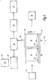
- each PCB 10 of a series of PCB's fed to a station 17 must be in a known orientation.
- the PCB's 10 are provided with registration holes 12 arranged to receive registration or data pins 14 on a table 15 at the station 17. Due to manufacturing tolerances, mere engagement of registration pins in registration holes is insufficient to ensure exact orientation and location of the PCB in accurate subsequent placement of components thereon.
- the station 17 is a viewing and comparing station. Discrepancies between the actual and intended position of the PCB and the location of surface characteristics (component locations) thereon can then be determined.
- the apparatus of the invention provides a feed position 20 whereat a next PCB 10, fed from a store 11, may be located.
- the table 15 is an X-Y table and serves to receive a PCB 10 from the feed position 20 in a position 22 wherein the PCB is mounted with its registration holes 12 engaged by the registration pins 14 of the table 15. The PCB 10 is clamped to the table 15 in such registered position.
- the table 15 carrying the clamped PCB 10 is moved to a position beneath a viewing head 24 and is stepped through a program (corresponding to, for example, the program for placing components on the board 10) which examines the surfaces characteristics e.g. component locations.
- the viewing head 24 comprises a video camera having a field of view matching at least the area of a location where a component is to be placed.
- the output of the camera is fed to a microprocessor where it is digitised on a pixel-by-pixel basis (the pixel size being determined by the degree of accuracy required for board adjustment).
- the pixel digital values are compared in the microprocessor 21 with corresponding values of a model (held in a store 23) of the viewed area of a "perfectly" positioned, zero manufacturing tolerance, board.
- the corresponding values are held in a store 23.
- the X-Y discrepancies, the error values, between the model and the true position of the surface characteristic (the component location) are determined by the microprocessor 21 and stored, for example on a floppy disc 13, the drive of which forms part of the store 23.
- the PCB 10 is then moved from the table 15 to a stack 19 and a next PCB 10 is then fed to the table 15 and its surface characteristics similarly compared, the differences (which may be in vector form) determined and stored on the disc 13, and this PCB 10 is then stacked. The process is repeated until the differences for each PCB 10 of the series has been determined.
- the stack 19 of PCB's 10 and the floppy disc can then be moved to a next stage 25 in the manufacturing process whereat each PCB 10 is placed on a registration table.
- Control means (not shown) reads the vector differences for that PCB, moves the registration table of the stage to position each PCB component location beneath a machine tool head of the stage which performs the appropriate operation e.g.
- the table of the stage 25 is then stepped (with the applied differences) to move the next component location of the PCB 10 beneath the machine tool head of the stage and so on.
- the board 10 is then moved to a next stage 27 of the manufacturing process.
- the mean vector difference between the true position of the board 10 and the desired position of the board 10 is determined. In this way, a "best fit" of the board area is determined. The differences are stored. The table 15 is then stepped through the rest of the program. At each step, discrepancies necessary to zero the position of the board 10 are determined, and stored. A mean vector difference may then be determined. The table 15 is then returned to alignment with the feed position 20.
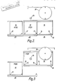
- each PCB 10 of a series of PCB's fed to the station must be in a known orientation.
- the PCB's 10 are again provided with registration holes 12 arranged to received registration or data pins 14 on a table 16 at the station 18.
- a viewing and comparing station 22 is included in the component placing station 18. Discrepancies between the actual and intended position of the PCB can then be determined and used immediately for component placement.
- the apparatus of this embodiment of the invention provides a feed position 20 whereat a next PCB 10, fed from a store (similar to the store 11), may be located.
- the table 16 is an X-Y table and serves to receive a PCB 10 from the feed position 20 in a first position 22 wherein the PCB is mounted with its registration holes 12 engaged by the registration pins 14 of the table 16. The PCB 10 is clamped to the table 16 in such registered position.
- the table 16 carrying the clamped PCB 10 is moved ( Figure 2) to a position beneath a viewing head 24 and is stepped through a program corresponding to the program for placing components on the board 10.
- the viewing head comprises a video camera having a field of view matching the area where a component is to be placed, the output of which is fed to a microprocessor similar to the microprocessor 21 of Figure 1 and digitised, on a pixel-by-pixel basis (the pixel size being determined by the degree of accuracy required for board adjustment).
- the pixel digital values are compared in the microprocessor with corresponding values (held in a store similar to the store 23 of Figure 1) of a model of the viewed area of a "perfectly" positioned, zero manufacturing tolerance, board and the X-Y discrepancies between the model and the viewed component location of the board area determined.
- the discrepancies are stored.
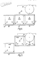
- the table 16 is then stepped through the rest of the program. At each step, discrepancies necessary to zero the position of the board 10 are determined, and stored. The table 16 is then returned to alignment with the feed position 20 ( Figure 4).
- the first board 10 is translated laterally from the first position 22 to a second position 26 and a next board 10 is fed from the feed position 20 to the first position 22.
- the first board 10 In its translation from the first to second position, the first board 10 is displaced in a predetermined direction and by a predetermined amount so that it retains its registration.
- the second board in its movement onto the table 16 from the feed position 20, is clamped into its registration position on the pins 14.
- the table 16 carrying the first board 10 in the second position 26 and the second board 10 in the first position 22 is moved to the position beneath the viewing head 24 and beneath a rotary assembly head 28.
- the table 16 is then stepped through its X-Y program appropriately modified by the stored X-Y discrepancies for each area where a component is to be placed.
- the head 28 is indexable and is arranged to insert components (not shown) into or onto the board 10 at the predetermined locations.
- the second board 10 is viewed by the camera 24 and its surface characteristics (located in the corrected position of the first board by virtue of the adjustment of the X-Y table 16) compared with the model.
- any further discrepancies on the second board between the "correct" position of the first board are noted and summed algebraically with the discrepancies of the first board. This may be effected by direct comparison with the original desired model or with the "stored" position of the first board now incorporated into the X-Y stepping program.
- the table After placement of the components on the first board and determination of X-Y discrepancies of the various locations of the second board, the table is moved back to its feed position. The first board is unclamped and fed therefrom. The second board is moved to the second position 26 and a third board is fed from the feed position 20 to the first position 22. The cycle is then repeated.
- the viewing area is relatively small, for example, 10 or 15mm square, the number of pixels necessary for accurate determination of the discrepancies is correspondingly reduced.
- A/D converters for digitising the pixel information need not be excessively fast to be able to process the viewed image in a time equal to or less than the component placement time. The production line is thus maintained at its normal through rate.
- the store may be temporary e.g. in RAM of the store 23 in which the vector differences can be used in a conjoined apparatus as shown in Figures 2 to 5 or, if a production line of linked apparatus (stages 25, 27 etc.) is provided, the microprocessor 21 may act as controller for all such linked apparatus.
- the vector differences can be stored on a floppy disc for use in subsequent manufacturing operations on separate machines having controllable tables for the PCB's.
- each PCB may have a machine readable print out of the vector differences or the mean vector difference applied thereto.
- each PCB is provided with a machine readable identifier e.g. a bar code number
- the vector differences and the identifier may be stored together (either temporarily in RAM or more permanently or a magnetic storage medium such as a floppy disc) and/or applied as a printed out machine readable label attached to the PCB 10.
- the automatic optical inspection station may be linked to other manufacturing apparatus or may be a stand alone unit. Out-of-tolerance PCB's can then be employed with much fewer rejects either of boards or, more costly, of boards with incorrectly placed components.
- viewing and comparison can be on the basis of the whole article or of a plurality of locations on the article.
- the stored discrepancies may be cumulative without reference to the model (save for the first article viewed).
Landscapes
- Engineering & Computer Science (AREA)
- Operations Research (AREA)
- Manufacturing & Machinery (AREA)
- Microelectronics & Electronic Packaging (AREA)
- Supply And Installment Of Electrical Components (AREA)
- Automatic Assembly (AREA)
Applications Claiming Priority (4)
| Application Number | Priority Date | Filing Date | Title |
|---|---|---|---|
| GB8811005 | 1988-05-10 | ||
| GB888811005A GB8811005D0 (en) | 1988-05-10 | 1988-05-10 | Improvements in/relating to methods/registration |
| GB8908505A GB2218509A (en) | 1988-05-10 | 1989-04-14 | Method of and apparatus for article registration |
| GB8908505 | 1989-04-14 |
Publications (2)
| Publication Number | Publication Date |
|---|---|
| EP0341944A2 true EP0341944A2 (de) | 1989-11-15 |
| EP0341944A3 EP0341944A3 (de) | 1991-06-26 |
Family
ID=26293874
Family Applications (1)
| Application Number | Title | Priority Date | Filing Date |
|---|---|---|---|
| EP19890304608 Withdrawn EP0341944A3 (de) | 1988-05-10 | 1989-05-08 | Verfahren und Vorrichtungen zur Positionserfassung |
Country Status (6)
| Country | Link |
|---|---|
| US (1) | US5134664A (de) |
| EP (1) | EP0341944A3 (de) |
| JP (1) | JPH0265930A (de) |
| DK (1) | DK226689A (de) |
| FI (1) | FI892235L (de) |
| PT (1) | PT90524A (de) |
Cited By (3)
| Publication number | Priority date | Publication date | Assignee | Title |
|---|---|---|---|---|
| EP0650319A1 (de) * | 1993-10-21 | 1995-04-26 | Tenryu Technics Co., Ltd. | Elektronische Bauteildatenschreiber und Bestücker, der diesen Schreiber verwendet |
| FR2741505A1 (fr) * | 1995-11-20 | 1997-05-23 | Magneti Marelli France | Substrat electronique comprenant un pion d'indexation mecanique |
| WO2000015017A1 (de) * | 1998-09-08 | 2000-03-16 | Siemens Production And Logistics Systems Ag | Verfahren und vorrichtung zum bearbeiten von substraten |
Families Citing this family (7)
| Publication number | Priority date | Publication date | Assignee | Title |
|---|---|---|---|---|
| US5495535A (en) * | 1992-01-31 | 1996-02-27 | Orbotech Ltd | Method of inspecting articles |
| US7286696B2 (en) * | 2000-10-18 | 2007-10-23 | Erickson Ronald R | Method and apparatus for utilizing representational images in commercial and other activities |
| US6581202B1 (en) * | 2000-11-10 | 2003-06-17 | Viasystems Group, Inc. | System and method for monitoring and improving dimensional stability and registration accuracy of multi-layer PCB manufacture |
| CN100561487C (zh) * | 2006-11-17 | 2009-11-18 | 鸿富锦精密工业(深圳)有限公司 | 具有多重负载拓扑布线架构的印刷电路板 |
| TWI499109B (zh) * | 2013-07-08 | 2015-09-01 | Chroma Ate Inc | A method of reading and writing fixture, machine table and alignment for flexible conductive circuit board |
| TWI724705B (zh) * | 2019-12-20 | 2021-04-11 | 財團法人工業技術研究院 | 工作件之設計圖像的補償方法及處理系統 |
| CN212990124U (zh) * | 2020-09-28 | 2021-04-16 | 苏州康代智能科技股份有限公司 | 一种pcb板自动读ocr码装置 |
Family Cites Families (13)
| Publication number | Priority date | Publication date | Assignee | Title |
|---|---|---|---|---|
| JPS5390577A (en) * | 1977-01-18 | 1978-08-09 | Matsushita Electric Ind Co Ltd | Apparatus for prepation unmerical control tape |
| JPS57103399A (en) * | 1980-12-18 | 1982-06-26 | Matsushita Electric Industrial Co Ltd | Device for mounting and inspecting leadless electronic part |
| US4481533A (en) * | 1981-11-27 | 1984-11-06 | Lenkeit Industries, Inc. | Method and apparatus for successively positioning sheets of material with precision for punching aligning holes in the sheets enabling the sheets to be used in the manufacture of composite circuit boards |
| GB8320016D0 (en) * | 1983-07-25 | 1983-08-24 | Lloyd Doyle Ltd | Apparatus for inspecting printed wiring boards |
| DE3377934D1 (en) * | 1983-12-28 | 1988-10-13 | Ibm | Process and equipment for the automatic alignment of an object in respect of a reference |
| IT1184602B (it) * | 1985-06-10 | 1987-10-28 | Ezio Curti | Procedimento e mezzi per stampare a registro il tracciato di un circuito elettronico rispetto a fori praticati in una piastra di supproto |
| JPH0679325B2 (ja) * | 1985-10-11 | 1994-10-05 | 株式会社日立製作所 | 位置姿勢判定方法 |
| US4680672A (en) * | 1985-11-08 | 1987-07-14 | Siemens-Allis | Molded case circuit breaker with front accessible control panel |
| US4799268A (en) * | 1985-11-12 | 1989-01-17 | Usm Corporation | Lead sense system for component insertion machine |
| US4821157A (en) * | 1986-02-21 | 1989-04-11 | Hewlett-Packard Co. | System for sensing and forming objects such as leads of electronic components |
| US4783826A (en) * | 1986-08-18 | 1988-11-08 | The Gerber Scientific Company, Inc. | Pattern inspection system |
| JPS6362242A (ja) * | 1986-09-02 | 1988-03-18 | Toshiba Corp | ワイヤボンディング装置 |
| US4811410A (en) * | 1986-12-08 | 1989-03-07 | American Telephone And Telegraph Company | Linescan inspection system for circuit boards |
-
1989
- 1989-05-08 EP EP19890304608 patent/EP0341944A3/de not_active Withdrawn
- 1989-05-09 DK DK226689A patent/DK226689A/da not_active Application Discontinuation
- 1989-05-09 FI FI892235A patent/FI892235L/fi not_active IP Right Cessation
- 1989-05-10 PT PT90524A patent/PT90524A/pt not_active Application Discontinuation
- 1989-05-10 JP JP1117177A patent/JPH0265930A/ja active Pending
-
1991
- 1991-10-22 US US07/780,458 patent/US5134664A/en not_active Expired - Fee Related
Cited By (5)
| Publication number | Priority date | Publication date | Assignee | Title |
|---|---|---|---|---|
| EP0650319A1 (de) * | 1993-10-21 | 1995-04-26 | Tenryu Technics Co., Ltd. | Elektronische Bauteildatenschreiber und Bestücker, der diesen Schreiber verwendet |
| US5646681A (en) * | 1993-10-21 | 1997-07-08 | Tenryu Technics Co., Ltd. | Electronic parts data recorder and a mounter employing the recorder |
| FR2741505A1 (fr) * | 1995-11-20 | 1997-05-23 | Magneti Marelli France | Substrat electronique comprenant un pion d'indexation mecanique |
| WO2000015017A1 (de) * | 1998-09-08 | 2000-03-16 | Siemens Production And Logistics Systems Ag | Verfahren und vorrichtung zum bearbeiten von substraten |
| US6079098A (en) * | 1998-09-08 | 2000-06-27 | Siemens Aktiengesellschaft | Method and apparatus for processing substrates |
Also Published As
| Publication number | Publication date |
|---|---|
| PT90524A (pt) | 1989-11-30 |
| JPH0265930A (ja) | 1990-03-06 |
| FI892235A7 (fi) | 1989-11-11 |
| FI892235L (fi) | 1989-11-11 |
| FI892235A0 (fi) | 1989-05-09 |
| DK226689A (da) | 1989-11-11 |
| DK226689D0 (da) | 1989-05-09 |
| EP0341944A3 (de) | 1991-06-26 |
| US5134664A (en) | 1992-07-28 |
Similar Documents
| Publication | Publication Date | Title |
|---|---|---|
| US6353312B1 (en) | Method for positioning a semiconductor die within a temporary package | |
| US5134664A (en) | Customized alignment for PCB assembly | |
| EP0772381A1 (de) | Verfahren und Vorrichtung zum Bestücken einer Leiterplatte mit elektronischen Bauteilen | |
| US7346420B2 (en) | Component feeder exchange diagnostic tool | |
| US4670981A (en) | Method of mounting electronic parts on the predetermined positions of a printed circuit board | |
| US6861269B2 (en) | Electric-circuit fabricating method and system, and electric-circuit fabricating program | |
| EP1187524B1 (de) | Verfahren und Einrichtung zur Montage von Bauteilen | |
| US20120015458A1 (en) | Mounting apparatus and mounting method | |
| US6647138B1 (en) | Electronic component mounting method and mounting apparatus | |
| US4922434A (en) | Linear interpolation for a component placement robot | |
| US5373633A (en) | Assembling method and apparatus for ink-jet head | |
| JPS63162141A (ja) | ワークピース位置決め方法 | |
| EP1629706B1 (de) | Verfahren zum zusammenbau einer schaltung | |
| US20020040519A1 (en) | Method of detecting position of printed-wiring board, and method and system for effecting working operation on the board, using detected board position | |
| GB2218509A (en) | Method of and apparatus for article registration | |
| US6885905B2 (en) | Electric-circuit fabricating system and method, and electric-circuit fabricating program | |
| CN112276508A (zh) | 一种内存卡的组装设备及组装方法 | |
| CN114993183A (zh) | 测试方法、存储装置、计算机设备及测试设备 | |
| JPH03281130A (ja) | 部品挿着装置 | |
| JP2773256B2 (ja) | 電子部品実装方法 | |
| JP3046283B2 (ja) | インクジェット用ヘッドの組立装置及び組立方法及びインクジェット用ヘッド | |
| US4550494A (en) | Automated printed circuit board assembly method | |
| JP2789761B2 (ja) | 電子部品の自動挿入方法 | |
| WO1998058527A1 (en) | Method for positioning of at least one component on a printed circuit board, method for handling a component and device for carrying out such method | |
| CN115038328A (zh) | 一种插件机的标定方法 |
Legal Events
| Date | Code | Title | Description |
|---|---|---|---|
| PUAI | Public reference made under article 153(3) epc to a published international application that has entered the european phase |
Free format text: ORIGINAL CODE: 0009012 |
|
| AK | Designated contracting states |
Kind code of ref document: A2 Designated state(s): BE DE ES FR GR IT LU NL SE |
|
| PUAL | Search report despatched |
Free format text: ORIGINAL CODE: 0009013 |
|
| AK | Designated contracting states |
Kind code of ref document: A3 Designated state(s): BE DE ES FR GR IT LU NL SE |
|
| 17P | Request for examination filed |
Effective date: 19910830 |
|
| 17Q | First examination report despatched |
Effective date: 19921127 |
|
| STAA | Information on the status of an ep patent application or granted ep patent |
Free format text: STATUS: THE APPLICATION IS DEEMED TO BE WITHDRAWN |
|
| 18D | Application deemed to be withdrawn |
Effective date: 19930907 |