EP0339529A2 - Amplificateur de tension alternative réglable - Google Patents
Amplificateur de tension alternative réglable Download PDFInfo
- Publication number
- EP0339529A2 EP0339529A2 EP19890107306 EP89107306A EP0339529A2 EP 0339529 A2 EP0339529 A2 EP 0339529A2 EP 19890107306 EP19890107306 EP 19890107306 EP 89107306 A EP89107306 A EP 89107306A EP 0339529 A2 EP0339529 A2 EP 0339529A2
- Authority
- EP
- European Patent Office
- Prior art keywords
- voltage
- gate
- effect transistor
- gate field
- amplifier
- Prior art date
- Legal status (The legal status is an assumption and is not a legal conclusion. Google has not performed a legal analysis and makes no representation as to the accuracy of the status listed.)
- Withdrawn
Links
Images

Classifications
-
- H—ELECTRICITY
- H03—ELECTRONIC CIRCUITRY
- H03G—CONTROL OF AMPLIFICATION
- H03G1/00—Details of arrangements for controlling amplification
- H03G1/0005—Circuits characterised by the type of controlling devices operated by a controlling current or voltage signal
- H03G1/0017—Circuits characterised by the type of controlling devices operated by a controlling current or voltage signal the device being at least one of the amplifying solid-state elements
- H03G1/0029—Circuits characterised by the type of controlling devices operated by a controlling current or voltage signal the device being at least one of the amplifying solid-state elements using field-effect transistors [FET]
Definitions
- the invention relates to an AC voltage amplifier, in particular a broadband amplifier for optical communications technology, with a single-gate field-effect transistor, to which the input voltage to be amplified is present on the gate side.
- AC amplifiers are those which contain a dual-gate field-effect transistor which operates in a frequency range from a few hertz to several gigahertz.
- a dual-gate field-effect transistor can be understood as a cascode circuit, represented by two single-gate transistors, the input transistor operating as a source circuit and the output transistor operating as a gate stage in the start-up area. Because of its complicated geometric structure, a dual-gate field-effect transistor achieves a lower cut-off frequency than a corresponding single-gate field-effect transistor if one imagines it to be composed of two single-gate field-effect transistors. In addition, the dual gate field effect transistor has a higher one Input capacitance than the single gate field effect transistor. In a dual-gate transistor, small currents can occur during the control process, which also flow in the gate stage. This reduces the cutoff frequency.
- This AC voltage amplifier does not allow a very large bandwidth and no great dynamics.
- the first object is achieved by an AC voltage amplifier of the type mentioned in the introduction of a first voltage generated from a combination of resistors and a second voltage on the gate side of the single-gate field-effect transistor, that the second voltage is opposite in sign and that the gain of the first single-gate field-effect transistor can be controlled via the second voltage
- any field effect transistor with a high transistor frequency can be used for the single gate field effect transistor, for example a high electron mobility transistor (HEMT).
- HEMT high electron mobility transistor
- the object according to claim 5 is achieved by a multi-stage amplifier in that it is constructed from a plurality of AC voltage amplifiers according to claim 1, each forming a single stage.
- the single-gate field-effect transistors of the individual stages operate at an almost constant drain-source voltage. They are controlled by transistors acting as current sources with a variable drain current in the pinch-off region of the drain-source voltage; the drain current is only dependent on the control voltage with which Transistors can be controlled.
- the basic circuit diagram shown in Fig. 1 contains a single gate field effect transistor F 1 in source circuit. At the same time there is a high-frequency alternating voltage U E and a negative constant voltage -U across a resistor R1 on it on the gate side.
- a resistor Z1 represents the input resistance of the circuit. It is coupled via the capacitor C1 to the gate of the transistor F1.
- a resistor Z2 forms an output load resistor and is connected via a capacitor C2 to the drain of the transistor F1.
- On the drain side via a resistor R D used for decoupling, there is also a positive, variable voltage + U.
- the ohmic resistor R D can be replaced by a broadband coil at higher frequencies; it also serves to adjust the gain.
- the output side voltage U A also contains no DC component due to the capacitor C2.
- Fig. 2 shows a single stage of the amplifier, which in addition to the resistors R1, R D , Z1, Z2 and the capacitors C1, C2 also contains a capacitor C3 and other resistors R2, R3, R4, with which the stage is voltage stabilized.
- part of the drain-source voltage U DS together with the voltage -U, which is an operating voltage -U here, is fed into the single-gate field-effect transistor at the gate and an optimal gate voltage is set at it.
- a capacitor C4 between the resistor R D and the source terminal of a further field effect transistor F ST is connected to the reference potential, so that only a direct voltage is present at the source terminal.
- the positive voltage + U is controlled without power by the field effect transistor F St , whose drain connection is connected to a constant voltage U o , while it is controlled on the gate side by a control voltage U St.
- the field effect transistor F St acts as a voltage source. If the voltage U o is not connected to the drain but to the source, it acts as a current source. In addition to a transistor F St , any other voltage and current sources are conceivable that allow the voltage + U to be controlled.
- This voltage U St can be generated, for example, in a control loop in which a comparison is made between the target and actual values of the output voltage U A.
- the current can also be controlled with a current source.
- a resistor R5 suppresses high-frequency vibrations.
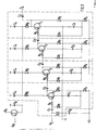
- a multi-stage amplifier (Fig. 3) consists of four stages, each of which contains a single gate field effect transistor F1, F2, F3, F4, each of which is connected via a drain resistor R D to the source terminal of the field effect transistor F St , so that all single-gate field effect transistors F1 to F4 a common, variable positive voltage + U is present. In this way, the dynamics of each single gate field effect transistor F1 to F4 is fully exploited.
- the resistors R3, Z1, Z2 are omitted.
- the drain-side capacitor C2 of each stage coincides with the gate-side capacitor C1 of the subsequent stage.
- Two capacitors C A , C B , and two capacitors C4, C3 set the AC voltage to the reference potential.
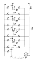
- the single-gate field effect transistors F1, F2, F3, F4 of a further, also four-stage multi-stage amplifier are source side through the drain current flowing through a resistor R7 an n-channel MOSFET enhancement field effect transistor controlled. This itself is controlled by a control voltage U St.
- One capacitor C5 is used on the source side of the single-gate field-effect transistors F1 to F4 for AC decoupling.
- An operating voltage source provides a negative, constant operating voltage -U, which drops to the gate terminals of the field effect transistors F1 to F4 through a resistor R6 and the resistor R5.
- the drain-side resistors R D are each connected in parallel to resistors R9 and with the Reference potential connected.
- a resistor R8 forms the input resistance of the amplifier circuit.
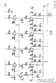
- a third, four-stage multi-stage amplifier (Fig. 5) contains as pnp bipolar transistors designed transistors T1 to T4 in the base circuit, each of which controls a single-gate field-effect transistor F1 to F4 through the respective resistor R D on the drain side.
- transistors T1 to T4 On the base side, transistors T1 to T4 have resistors R10 connected upstream; They are connected to the reference potential via a capacitor C6. Your base voltage is supplied from a control transistor T St collector side, which in turn is controlled by a control voltage U St base side and whose emitter is connected via a resistor R13 to the reference potential.
- the transistors T1 to T4 is on the emitter side via a resistor R11 to the constant voltage + U, which is also applied via a resistor R12 to the collector of the control transistor T St.
- the gate voltage is generated via the resistors R1, R2, R4.
- the capacitor C4 sets the constant, negative voltage -U in terms of AC voltage to the reference potential.
- the field effect transistors F1 to F4 are connected to the reference potential via the resistors R1, R5 and a capacitor C7.
- the AC voltage U E is coupled into the multi-stage amplifier via the capacitor C 1.
- a resistor R14 represents the input resistance of the multi-stage amplifier.
- the drain-source voltage U DS of the single-gate field-effect transistors F1 to F4 is set so that it lies in the pinch-off area; then can be almost completely independent of the drain-source voltage U DS, the drain current impress the transistors T1 to T4.
- field effect transistors or Darlington circuits can also be inserted in the network.
Landscapes
- Amplifiers (AREA)
- Control Of Amplification And Gain Control (AREA)
Applications Claiming Priority (2)
| Application Number | Priority Date | Filing Date | Title |
|---|---|---|---|
| DE3814041 | 1988-04-26 | ||
| DE3814041A DE3814041A1 (de) | 1988-04-26 | 1988-04-26 | Steuerbarer wechselspannungsverstaerker |
Publications (2)
| Publication Number | Publication Date |
|---|---|
| EP0339529A2 true EP0339529A2 (fr) | 1989-11-02 |
| EP0339529A3 EP0339529A3 (fr) | 1991-03-20 |
Family
ID=6352897
Family Applications (1)
| Application Number | Title | Priority Date | Filing Date |
|---|---|---|---|
| EP19890107306 Withdrawn EP0339529A3 (fr) | 1988-04-26 | 1989-04-22 | Amplificateur de tension alternative réglable |
Country Status (5)
| Country | Link |
|---|---|
| US (1) | US4943785A (fr) |
| EP (1) | EP0339529A3 (fr) |
| AU (1) | AU614828B2 (fr) |
| CA (1) | CA1319178C (fr) |
| DE (1) | DE3814041A1 (fr) |
Cited By (1)
| Publication number | Priority date | Publication date | Assignee | Title |
|---|---|---|---|---|
| EP0435048A3 (en) * | 1989-12-23 | 1991-12-04 | Standard Elektrik Lorenz Aktiengesellschaft | Broadband amplifier stage with controllable amplification |
Families Citing this family (3)
| Publication number | Priority date | Publication date | Assignee | Title |
|---|---|---|---|---|
| FI82333C (fi) * | 1989-04-24 | 1991-02-11 | Telenokia Oy | Radiosaendares hoegfrekvensfoerstaerkare. |
| JP3508401B2 (ja) * | 1996-07-12 | 2004-03-22 | 富士通株式会社 | 増幅回路および多段増幅回路 |
| GB0027067D0 (en) * | 2000-11-06 | 2000-12-20 | Nokia Networks Oy | Amplifier linearisation |
Family Cites Families (17)
| Publication number | Priority date | Publication date | Assignee | Title |
|---|---|---|---|---|
| US3286189A (en) * | 1964-01-20 | 1966-11-15 | Ithaco | High gain field-effect transistor-loaded amplifier |
| GB1178232A (en) * | 1966-02-12 | 1970-01-21 | Emi Ltd | Improvements in or relating to gain control circuits. |
| DE1591506A1 (fr) * | 1966-06-13 | |||
| US3462701A (en) * | 1967-01-26 | 1969-08-19 | Honeywell Inc | Biasing circuit for use with field-effect transistors |
| US3914702A (en) * | 1973-06-01 | 1975-10-21 | Rca Corp | Complementary field-effect transistor amplifier |
| GB2002608B (en) * | 1977-08-01 | 1982-03-24 | Pioneer Electronic Corp | Automatic gain control circuit |
| US4255716A (en) * | 1977-09-10 | 1981-03-10 | Tokyo Shibaura Denki Kabushiki Kaisha | Automatic gain control circuit |
| JPS55112010A (en) * | 1979-02-22 | 1980-08-29 | Haruaki Tamaoki | Amplifier circuit by fet |
| NL8001117A (nl) * | 1980-02-25 | 1981-09-16 | Philips Nv | Versterkertrap met regelbare versterkingsfaktor uitgevoerd met veldeffekttransistoren. |
| FR2512292B1 (fr) * | 1981-08-25 | 1986-11-21 | Lmt Radio Professionelle | Amplificateur hyperfrequence a transistors a effet de champ, notamment pour radar doppler |
| DE3204839C2 (de) * | 1982-02-11 | 1984-04-26 | Siemens AG, 1000 Berlin und 8000 München | Fotodiodenverstärker mit großem Dynamikbereich |
| DE3207945A1 (de) * | 1982-03-05 | 1983-09-15 | Licentia Patent-Verwaltungs-Gmbh, 6000 Frankfurt | Regelbarer hochfrequenzverstaerker |
| GB2117583B (en) * | 1982-03-31 | 1986-01-29 | Ferranti Plc | Gain control circuit |
| US4420724A (en) * | 1982-05-17 | 1983-12-13 | Bell Telephone Laboratories, Incorporated | FET Amplifier with wide dynamic range |
| JPS5981113U (ja) * | 1982-11-25 | 1984-06-01 | 日本電気株式会社 | 出力電力制御回路 |
| JPS60235513A (ja) * | 1984-05-08 | 1985-11-22 | Nec Corp | 増幅回路 |
| GB2176962B (en) * | 1985-06-21 | 1988-12-29 | Stc Plc | Pinfet receiver |
-
1988
- 1988-04-26 DE DE3814041A patent/DE3814041A1/de not_active Withdrawn
-
1989
- 1989-04-18 AU AU33103/89A patent/AU614828B2/en not_active Ceased
- 1989-04-19 US US07/340,336 patent/US4943785A/en not_active Expired - Fee Related
- 1989-04-21 CA CA000597395A patent/CA1319178C/fr not_active Expired - Fee Related
- 1989-04-22 EP EP19890107306 patent/EP0339529A3/fr not_active Withdrawn
Cited By (1)
| Publication number | Priority date | Publication date | Assignee | Title |
|---|---|---|---|---|
| EP0435048A3 (en) * | 1989-12-23 | 1991-12-04 | Standard Elektrik Lorenz Aktiengesellschaft | Broadband amplifier stage with controllable amplification |
Also Published As
| Publication number | Publication date |
|---|---|
| AU3310389A (en) | 1989-11-02 |
| CA1319178C (fr) | 1993-06-15 |
| US4943785A (en) | 1990-07-24 |
| EP0339529A3 (fr) | 1991-03-20 |
| DE3814041A1 (de) | 1989-11-09 |
| AU614828B2 (en) | 1991-09-12 |
Similar Documents
| Publication | Publication Date | Title |
|---|---|---|
| DE69022108T2 (de) | Verstärkeranordnung. | |
| DE69506727T2 (de) | Geräuscharme verstärker für mikrofon | |
| DE60132860T2 (de) | Transkonduktanzverstärker | |
| CH625095A5 (fr) | ||
| WO2007118540A1 (fr) | Miroir de courant CMOS rapide | |
| DE2920793C2 (de) | Linearer Gegentakt-B-Verstärker | |
| DE3736380C2 (de) | Verstärker | |
| DE69201297T2 (de) | Ultraschnelle Differenzverstärker. | |
| DE3586368T2 (de) | Hochfrequenzverstaerker. | |
| EP0363714B1 (fr) | Amplificateur de compression intégré avec une tension de seuil programmable | |
| EP0077500A2 (fr) | Diviseur de fréquence intégrable | |
| EP0339529A2 (fr) | Amplificateur de tension alternative réglable | |
| DE69413235T2 (de) | In verschiedene Konfigurationen umschaltbarer Operationsverstärker | |
| EP0685782B1 (fr) | Regulateur de tension | |
| DE19841677B4 (de) | Integrierte, aktive Intergrator-Filterschaltung | |
| DE3436302A1 (de) | Rauschfreie, die bauelementflaeche beeinflussende kaskodenschaltung | |
| DE3721221C2 (de) | Spannungsverstärkerschaltung geringer Klirrverzerrung für widerstandsbehaftete Lasten | |
| DE10241813A1 (de) | Verstärker | |
| DE3624391C2 (fr) | ||
| EP0632580A2 (fr) | Etage de sortie amplificateur | |
| DE3724980A1 (de) | Spannungswiederholerschaltung fuer eine ohmsche komponente aufweisende last mit kompensation der oberwellenverzerrung | |
| DE69228450T2 (de) | Schnelle Pufferschaltung | |
| EP1187315B1 (fr) | Amplificateur opérationnel commutable pour applications dans un amplificateur opérationnel de commutation | |
| DE4431466C1 (de) | Spannungsregler | |
| DE2711520C3 (de) | Belastungsschaltung für eine Signalquelle |
Legal Events
| Date | Code | Title | Description |
|---|---|---|---|
| PUAI | Public reference made under article 153(3) epc to a published international application that has entered the european phase |
Free format text: ORIGINAL CODE: 0009012 |
|
| AK | Designated contracting states |
Kind code of ref document: A2 Designated state(s): AT BE CH DE ES FR GB IT LI NL SE |
|
| PUAL | Search report despatched |
Free format text: ORIGINAL CODE: 0009013 |
|
| AK | Designated contracting states |
Kind code of ref document: A3 Designated state(s): AT BE CH DE ES FR GB IT LI NL SE |
|
| 17P | Request for examination filed |
Effective date: 19910803 |
|
| RAP3 | Party data changed (applicant data changed or rights of an application transferred) |
Owner name: ALCATEL N.V. Owner name: ALCATEL SEL AKTIENGESELLSCHAFT |
|
| 17Q | First examination report despatched |
Effective date: 19940121 |
|
| GRAG | Despatch of communication of intention to grant |
Free format text: ORIGINAL CODE: EPIDOS AGRA |
|
| GRAG | Despatch of communication of intention to grant |
Free format text: ORIGINAL CODE: EPIDOS AGRA |
|
| GRAH | Despatch of communication of intention to grant a patent |
Free format text: ORIGINAL CODE: EPIDOS IGRA |
|
| STAA | Information on the status of an ep patent application or granted ep patent |
Free format text: STATUS: THE APPLICATION IS DEEMED TO BE WITHDRAWN |
|
| 18D | Application deemed to be withdrawn |
Effective date: 19980402 |