EP0339529A2 - Controllable ac-amplifier - Google Patents
Controllable ac-amplifier Download PDFInfo
- Publication number
- EP0339529A2 EP0339529A2 EP19890107306 EP89107306A EP0339529A2 EP 0339529 A2 EP0339529 A2 EP 0339529A2 EP 19890107306 EP19890107306 EP 19890107306 EP 89107306 A EP89107306 A EP 89107306A EP 0339529 A2 EP0339529 A2 EP 0339529A2
- Authority
- EP
- European Patent Office
- Prior art keywords
- voltage
- gate
- effect transistor
- gate field
- amplifier
- Prior art date
- Legal status (The legal status is an assumption and is not a legal conclusion. Google has not performed a legal analysis and makes no representation as to the accuracy of the status listed.)
- Withdrawn
Links
Images

Classifications
-
- H—ELECTRICITY
- H03—ELECTRONIC CIRCUITRY
- H03G—CONTROL OF AMPLIFICATION
- H03G1/00—Details of arrangements for controlling amplification
- H03G1/0005—Circuits characterised by the type of controlling devices operated by a controlling current or voltage signal
- H03G1/0017—Circuits characterised by the type of controlling devices operated by a controlling current or voltage signal the device being at least one of the amplifying solid state elements of the amplifier
- H03G1/0029—Circuits characterised by the type of controlling devices operated by a controlling current or voltage signal the device being at least one of the amplifying solid state elements of the amplifier using FETs
Definitions
- the invention relates to an AC voltage amplifier, in particular a broadband amplifier for optical communications technology, with a single-gate field-effect transistor, to which the input voltage to be amplified is present on the gate side.
- AC amplifiers are those which contain a dual-gate field-effect transistor which operates in a frequency range from a few hertz to several gigahertz.
- a dual-gate field-effect transistor can be understood as a cascode circuit, represented by two single-gate transistors, the input transistor operating as a source circuit and the output transistor operating as a gate stage in the start-up area. Because of its complicated geometric structure, a dual-gate field-effect transistor achieves a lower cut-off frequency than a corresponding single-gate field-effect transistor if one imagines it to be composed of two single-gate field-effect transistors. In addition, the dual gate field effect transistor has a higher one Input capacitance than the single gate field effect transistor. In a dual-gate transistor, small currents can occur during the control process, which also flow in the gate stage. This reduces the cutoff frequency.
- This AC voltage amplifier does not allow a very large bandwidth and no great dynamics.
- the first object is achieved by an AC voltage amplifier of the type mentioned in the introduction of a first voltage generated from a combination of resistors and a second voltage on the gate side of the single-gate field-effect transistor, that the second voltage is opposite in sign and that the gain of the first single-gate field-effect transistor can be controlled via the second voltage
- any field effect transistor with a high transistor frequency can be used for the single gate field effect transistor, for example a high electron mobility transistor (HEMT).
- HEMT high electron mobility transistor
- the object according to claim 5 is achieved by a multi-stage amplifier in that it is constructed from a plurality of AC voltage amplifiers according to claim 1, each forming a single stage.
- the single-gate field-effect transistors of the individual stages operate at an almost constant drain-source voltage. They are controlled by transistors acting as current sources with a variable drain current in the pinch-off region of the drain-source voltage; the drain current is only dependent on the control voltage with which Transistors can be controlled.
- the basic circuit diagram shown in Fig. 1 contains a single gate field effect transistor F 1 in source circuit. At the same time there is a high-frequency alternating voltage U E and a negative constant voltage -U across a resistor R1 on it on the gate side.
- a resistor Z1 represents the input resistance of the circuit. It is coupled via the capacitor C1 to the gate of the transistor F1.
- a resistor Z2 forms an output load resistor and is connected via a capacitor C2 to the drain of the transistor F1.
- On the drain side via a resistor R D used for decoupling, there is also a positive, variable voltage + U.
- the ohmic resistor R D can be replaced by a broadband coil at higher frequencies; it also serves to adjust the gain.
- the output side voltage U A also contains no DC component due to the capacitor C2.
- Fig. 2 shows a single stage of the amplifier, which in addition to the resistors R1, R D , Z1, Z2 and the capacitors C1, C2 also contains a capacitor C3 and other resistors R2, R3, R4, with which the stage is voltage stabilized.
- part of the drain-source voltage U DS together with the voltage -U, which is an operating voltage -U here, is fed into the single-gate field-effect transistor at the gate and an optimal gate voltage is set at it.
- a capacitor C4 between the resistor R D and the source terminal of a further field effect transistor F ST is connected to the reference potential, so that only a direct voltage is present at the source terminal.
- the positive voltage + U is controlled without power by the field effect transistor F St , whose drain connection is connected to a constant voltage U o , while it is controlled on the gate side by a control voltage U St.
- the field effect transistor F St acts as a voltage source. If the voltage U o is not connected to the drain but to the source, it acts as a current source. In addition to a transistor F St , any other voltage and current sources are conceivable that allow the voltage + U to be controlled.
- This voltage U St can be generated, for example, in a control loop in which a comparison is made between the target and actual values of the output voltage U A.
- the current can also be controlled with a current source.
- a resistor R5 suppresses high-frequency vibrations.
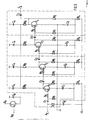
- a multi-stage amplifier (Fig. 3) consists of four stages, each of which contains a single gate field effect transistor F1, F2, F3, F4, each of which is connected via a drain resistor R D to the source terminal of the field effect transistor F St , so that all single-gate field effect transistors F1 to F4 a common, variable positive voltage + U is present. In this way, the dynamics of each single gate field effect transistor F1 to F4 is fully exploited.
- the resistors R3, Z1, Z2 are omitted.
- the drain-side capacitor C2 of each stage coincides with the gate-side capacitor C1 of the subsequent stage.
- Two capacitors C A , C B , and two capacitors C4, C3 set the AC voltage to the reference potential.
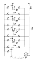
- the single-gate field effect transistors F1, F2, F3, F4 of a further, also four-stage multi-stage amplifier are source side through the drain current flowing through a resistor R7 an n-channel MOSFET enhancement field effect transistor controlled. This itself is controlled by a control voltage U St.
- One capacitor C5 is used on the source side of the single-gate field-effect transistors F1 to F4 for AC decoupling.
- An operating voltage source provides a negative, constant operating voltage -U, which drops to the gate terminals of the field effect transistors F1 to F4 through a resistor R6 and the resistor R5.
- the drain-side resistors R D are each connected in parallel to resistors R9 and with the Reference potential connected.
- a resistor R8 forms the input resistance of the amplifier circuit.
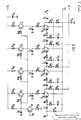
- a third, four-stage multi-stage amplifier (Fig. 5) contains as pnp bipolar transistors designed transistors T1 to T4 in the base circuit, each of which controls a single-gate field-effect transistor F1 to F4 through the respective resistor R D on the drain side.
- transistors T1 to T4 On the base side, transistors T1 to T4 have resistors R10 connected upstream; They are connected to the reference potential via a capacitor C6. Your base voltage is supplied from a control transistor T St collector side, which in turn is controlled by a control voltage U St base side and whose emitter is connected via a resistor R13 to the reference potential.
- the transistors T1 to T4 is on the emitter side via a resistor R11 to the constant voltage + U, which is also applied via a resistor R12 to the collector of the control transistor T St.
- the gate voltage is generated via the resistors R1, R2, R4.
- the capacitor C4 sets the constant, negative voltage -U in terms of AC voltage to the reference potential.
- the field effect transistors F1 to F4 are connected to the reference potential via the resistors R1, R5 and a capacitor C7.
- the AC voltage U E is coupled into the multi-stage amplifier via the capacitor C 1.
- a resistor R14 represents the input resistance of the multi-stage amplifier.
- the drain-source voltage U DS of the single-gate field-effect transistors F1 to F4 is set so that it lies in the pinch-off area; then can be almost completely independent of the drain-source voltage U DS, the drain current impress the transistors T1 to T4.
- field effect transistors or Darlington circuits can also be inserted in the network.
Abstract
Description
Die Erfindung betrifft einen Wechselspannungsverstärker, insbesondere Breitbandverstärker für die optische Nachrichtentechnik, mit einem Single-Gate-Feldeffekttransistor, an dem gateseitig die zu verstärkende Eingangsspannung anliegt.The invention relates to an AC voltage amplifier, in particular a broadband amplifier for optical communications technology, with a single-gate field-effect transistor, to which the input voltage to be amplified is present on the gate side.
Als Wechselspannungsverstärker sind solche bekannt, die einen Dual-Gate-Feldeffekttransistor enthalten, welcher etwa in einem Frequenzbereich von wenigen Hertz bis zu mehreren Gigahertz arbeitet.Known as AC amplifiers are those which contain a dual-gate field-effect transistor which operates in a frequency range from a few hertz to several gigahertz.
Ein Dual-Gate-Feldeffekttransistor läßt sich auffassen als Kaskodeschaltung, dargestellt durch zwei Single-Gate-Transistoren, wobei der Eingangstransistor in Sourceschaltung, der Ausgangstransistor als Gatestufe im Anlaufbereich arbeitet. Ein Dual-Gate-Feldeffekttransistor erreicht wegen seiner komplizierten geometrischen Struktur eine kleinere Grenzfrequenz als ein entsprechender Single-Gate-Feldeffekttransistor, wenn man sich ihn als aus zwei Single-Gate-Feldeffekttransistoren zusammengesetzt vorstellt. Außerdem hat der Dual-Gate-Feldeffekttransistor eine höhere Eingangskapazität als der Single-Gate-Feldeffekttransistor. In einem Dual-Gate-Transistor können beim Steuervorgang kleine Ströme auftreten, die auch in der Gatestufe fließen. Dadurch geht die Grenzfrequenz zurück.A dual-gate field-effect transistor can be understood as a cascode circuit, represented by two single-gate transistors, the input transistor operating as a source circuit and the output transistor operating as a gate stage in the start-up area. Because of its complicated geometric structure, a dual-gate field-effect transistor achieves a lower cut-off frequency than a corresponding single-gate field-effect transistor if one imagines it to be composed of two single-gate field-effect transistors. In addition, the dual gate field effect transistor has a higher one Input capacitance than the single gate field effect transistor. In a dual-gate transistor, small currents can occur during the control process, which also flow in the gate stage. This reduces the cutoff frequency.
Dieser Wechselspannungsverstärker läßt keine sehr große Bandbreite und keine große Dynamik zu.This AC voltage amplifier does not allow a very large bandwidth and no great dynamics.
Es ist die erste Aufgabe der Erfindung, einen Wechselspannungsverstärker zu schaffen, der steuerbar ist und nicht die Nachteile eines Wechselspannungsverstärkers mit einem Dual-Gate-Feldeffekttransistor hat.It is the first object of the invention to provide an AC amplifier that is controllable and does not have the disadvantages of an AC amplifier with a dual gate field effect transistor.
Außerdem ist es die Aufgabe der Erfindung, einen steuerbaren Mehrstufenverstärker zu schaffen.It is also an object of the invention to provide a controllable multi-stage amplifier.
Die erste Aufgabe wird durch einen Wechselspannungsverstärker der eingangs genannten Art dadurch gelöst, daß an dem Single-Gate-Feldeffekttransistor gateseitig eine erste, aus einer Widerstandkombination erzeugte Spannung und drainseitig eine zweite Spannung anliegen, daß die zweite Spannung der ersten Spannung im Vorzeichen entgegengesetzt ist und daß über die zweite Spannung die Verstärkung des ersten Single-Gate-Feldeffekttransistors Steuerbar istThe first object is achieved by an AC voltage amplifier of the type mentioned in the introduction of a first voltage generated from a combination of resistors and a second voltage on the gate side of the single-gate field-effect transistor, that the second voltage is opposite in sign and that the gain of the first single-gate field-effect transistor can be controlled via the second voltage
Vorteilhaft ist, daß sich für den Single-Gate-Feldeffekttransistor jeder Feldeffekttransistor mit einer hohen Transistorfrequenz einsetzen läßt, z.B. ein High Electon Mobility Transistor (HEMT)It is advantageous that any field effect transistor with a high transistor frequency can be used for the single gate field effect transistor, for example a high electron mobility transistor (HEMT).
Weiterbildungen ergeben sich aus den Unteransprüchen 2 bis 4.Further developments result from subclaims 2 to 4.
Vorteilhaft ist, daß der an diesem Wechselspannungsverstärker anliegende Lastwiderstand nahezu frequenzunabhängig ist. Während sich die Grenzfrequenz als Funktion der Spannung in einer Kaskodenschaltung, wie sie der Dual-Gate-Feldeffekttransistor darstellt, zweifach ändert, wird gemäß der Erfindung nur ein einziger Transistor höherer Grenzfrequenz gesteuert.It is advantageous that the load resistance applied to this AC voltage amplifier is almost independent of frequency. While the cut-off frequency changes twice as a function of the voltage in a cascode circuit, as represented by the dual-gate field-effect transistor, only a single transistor of a higher cut-off frequency is controlled according to the invention.
Außerdem wird die Aufgabe nach Anspruch 5 durch einen Mehrstufenverstärker dadurch gelöst, daß er aus mehreren, je eine Einzelstufe bildenden Wechselspannungsverstärkern nach Anspruch 1 aufgebaut ist.In addition, the object according to
Eine Weiterbildung ergibt sich aus Unteranspruch 6.A further development results from subclaim 6.
Weitere Mehrstufenverstärker ergeben sich aus den Ansprüchen 7 und 8.Further multi-stage amplifiers result from claims 7 and 8.
Gemäß Anspruch 8 arbeiten die Single-Gate-Feldeffekttransistoren der einzelnen Stufen bei nahezu konstanter Drain-Source-Spannung. Sie werden von als Stromquellen wirkenden Transistoren mit einem veränderbaren Drain-Strom im Abschnürbereich der Drain-Source-Spannung gesteuert; der Drain-Strom ist nur davon abhängig, mit welcher Steuerspannung die Transistoren gesteuert werden.According to claim 8, the single-gate field-effect transistors of the individual stages operate at an almost constant drain-source voltage. They are controlled by transistors acting as current sources with a variable drain current in the pinch-off region of the drain-source voltage; the drain current is only dependent on the control voltage with which Transistors can be controlled.
Die Erfindung wird anhand der Figuren in Beispielen erläutert. Es zeigen:
- Fig 1 das Prinzip der Verstärkerschaltung mit einem Single-Gate-Feldeffekttransistor in Sourceschaltung;
- Fig 2 ein Ausführungsbeispiel des Verstärkers in einer Einzelstufe, den Single-Gate-Feldeffekttransistor aus Fig. 1 enthaltend, mit einem weiteren Feldeffekttransistor zur Spannungssteuerung;
- Fig 3 einen Mehrstufenverstärker mit vier Einzelstufen, deren jede einen Single-Gate-Feldeffekttransistor aus Fig. 2 enthält, und mit dem Feldeffekttransistor zur drainseitigen Steuerung;
- Fig 4 einen Mehrstufenverstärker mit vier Einzelstufen, deren jede einen Single-Gate-Feldeffekttransistor aus Fig. 2 enthält, und mit dem Feldeffekttransistor zur sourceseitigen Steuerung und
- Fig 5 einen Mehrstufenverstärker mit vier Einzelstufen, deren jede einen Single-Gate-Feldeffekttransistor aus Fig. 2 und einen Bipolartransistor als Stromquelle zur drainseitigen Steuerung enthält.
- 1 shows the principle of the amplifier circuit with a single-gate field-effect transistor in a source circuit;
- 2 shows an exemplary embodiment of the amplifier in a single stage, containing the single-gate field-effect transistor from FIG. 1, with a further field-effect transistor for voltage control;
- 3 shows a multistage amplifier with four individual stages, each of which contains a single-gate field-effect transistor from FIG. 2, and with the field-effect transistor for drain-side control;
- 4 shows a multi-stage amplifier with four individual stages, each of which contains a single-gate field-effect transistor from FIG. 2, and with the field-effect transistor for control on the source side and
- 5 shows a multi-stage amplifier with four individual stages, each of which has a single-gate field-effect transistor from FIG. 2 and a bipolar transistor as a current source control on the drain side.
Das in Fig. 1 gezeigte Prinzipschaltbild enthält einen Single-Gate-Feldeffekttransistor F₁ in Sourceschaltung. Gleichzeitig liegen an ihm gateseitig über einen Kondensator C₁ eine hochfrequente Wechselspannung UE und über einen Widerstand R₁ eine negative, konstante Spannung -U an. Ein Widerstand Z₁ stellt den Eingangswiderstand der Schaltung dar. Er wird über den Kondensator C₁ an das Gate des Transistors F₁ angekoppelt. Ein Widerstand Z₂ bildet einen Ausgangslastwiderstand und ist über einen Kondensator C₂ mit dem Drainanschluß des Transistors F₁ verbunden. Drainseitig, über einen zur Entkopplung dienenden Widerstand RD, liegt ferner eine positive, veränderliche Spannung +U an. Der ohmsche Widerstand RD kann bei höheren Frequenzen durch eine Breitbandspule ersetzt werden; er dient zudem zur Verstärkungseinstellung.The basic circuit diagram shown in Fig. 1 contains a single gate field
Daß die Spannungen +U, -U positiv bzw. negativ sind, gilt nur im Fall eines n-Kanal-Single-Gate-Feldeffekttransistors F₁; bei einem p-Kanal-Transistor müssen sie umgekehrte Polaritäten haben.That the voltages + U, -U are positive or negative applies only in the case of an n-channel single-gate field-effect transistor F₁; with a p-channel transistor, they must have opposite polarities.
Die ausgangsseitige Spannung UA enthält wegen des Kondensators C₂ ebenfalls keinen Gleichstromanteil.The output side voltage U A also contains no DC component due to the capacitor C₂.
Fig. 2 zeigt eine Einzelstufe des Verstärkers, die neben den Widerständen R₁, RD, Z₁, Z₂ sowie den Kondensatoren C₁, C₂ noch einen Kondensator C₃ und weitere Widerstände R₂, R₃, R₄ enthält, mit denen die Stufe spannungsstabilisiert wird. Auf diese Weise wird ein Teil der Drain-Source-Spannung UDS zusammen mit der Spannung -U, die hier eine Betriebsspannung -U ist, gateseitig in den Single-Gate-Feldeffekttransistor eingespeist und eine optimale Gatespannung an ihm eingestellt. Ein Kondensator C₄ zwischen dem Widerstand RD und dem Soureeanschluß eines weiteren Feldeffekttransistors FST ist mit dem Bezugspotential verbunden, so daß an dem Sourceanschluß nur eine Gleichspannung an liegt.Fig. 2 shows a single stage of the amplifier, which in addition to the resistors R₁, R D , Z₁, Z₂ and the capacitors C₁, C₂ also contains a capacitor C₃ and other resistors R₂, R₃, R₄, with which the stage is voltage stabilized. In this way part of the drain-source voltage U DS together with the voltage -U, which is an operating voltage -U here, is fed into the single-gate field-effect transistor at the gate and an optimal gate voltage is set at it. A capacitor C₄ between the resistor R D and the source terminal of a further field effect transistor F ST is connected to the reference potential, so that only a direct voltage is present at the source terminal.
Die positive Spannung +U wird in diesem Fall von dem Feldeffekttransistor FSt leistungslos gesteuert, dessen Drainanschluß mit einer konstanten Spannung Uo verbunden ist, während er gateseitig durch eine Steuerspannung USt gesteuert wird.In this case, the positive voltage + U is controlled without power by the field effect transistor F St , whose drain connection is connected to a constant voltage U o , while it is controlled on the gate side by a control voltage U St.
In diesem Fall wirkt der Feldeffekttransistor FSt als Spannungsquelle. Wenn die Spannung Uo nicht drain-, sondern sourceseitig angeschlossen ist, wirkt er als Stromquelle. Außer einem Transistor FSt sind beliebige andere Spannungs- und Stromquellen denkbar, die die Steuerung der Spannung +U gestatten. Diese Spannung USt kann etwa in einem Regelkreis erzeugt werden, in welchem ein Vergleich zwischen Soll- und Ist-Wert der Ausgangsspannung UA erfolgt.In this case, the field effect transistor F St acts as a voltage source. If the voltage U o is not connected to the drain but to the source, it acts as a current source. In addition to a transistor F St , any other voltage and current sources are conceivable that allow the voltage + U to be controlled. This voltage U St can be generated, for example, in a control loop in which a comparison is made between the target and actual values of the output voltage U A.
Ein Ändern der Spannung +U mittels des Feldeffekttransistors FSt bewirkt, daß der Drain-Strom am Single-Gate-Feldeffekttransistor F₁ ebenfalls variiert wird. Dieser arbeitet dann in einem Bereich variabler Steilheit
Anstelle der Spannungssteuerung durch den Feldeffekttransistor FST läßt sich mit einer Stromquelle auch der Strom steuern.Instead of the voltage control by the field effect transistor F ST , the current can also be controlled with a current source.
Ein Widerstand R₅ unterdrückt hochfrequente Schwingungen.A resistor R₅ suppresses high-frequency vibrations.
Ein Mehrstufenverstärker (Fig. 3) besteht aus vier Stufen, deren jede einen Single-Gate-Feldeffekttransistor F₁, F₂, F₃, F₄ enthält, der jeweils über einen drainseitigen Widerstand RD mit dem Sourceanschluß des Feldeffekttransistors FSt verbunden ist, so daß an allen Single-Gate-Feldeffekttransistoren F₁ bis F₄ eine gemeinsame, veränderliche positive Spannung +U anliegt. Auf diese Weise wird die Dynamik jedes einzelnen Single-Gate-Feldeffekttransistors F₁ bis F₄ voll ausgeschöpft.A multi-stage amplifier (Fig. 3) consists of four stages, each of which contains a single gate field effect transistor F₁, F₂, F₃, F₄, each of which is connected via a drain resistor R D to the source terminal of the field effect transistor F St , so that all single-gate field effect transistors F₁ to F₄ a common, variable positive voltage + U is present. In this way, the dynamics of each single gate field effect transistor F₁ to F₄ is fully exploited.
Bis auf den Widerstand Z₁ vor der ersten Stufe entfallen die Widerstände R₃, Z₁, Z₂. Der drainseitige Kondensator C₂ jeder Stufe fällt mit dem gateseitigen Kondensator C₁ der jeweils nachfolgenden Stufe zusammen.Except for the resistor Z₁ before the first stage, the resistors R₃, Z₁, Z₂ are omitted. The drain-side capacitor C₂ of each stage coincides with the gate-side capacitor C₁ of the subsequent stage.
Zwei Kondensatoren CA, CB, sowie je Stufe zwei Kondensatoren C₄, C₃ legen die Wechselspannung auf das Bezugspotential.Two capacitors C A , C B , and two capacitors C₄, C₃ set the AC voltage to the reference potential.
Die Single-Gate-Feldeffekttransistoren F₁, F₂, F₃, F₄ eines weiteren, ebenfalls vierstufigen Mehrstufenverstärkers (Fig. 4) werden sourceseitig durch den über einen Widerstand R₇ fließenden Drainstrom eines n-Kanal-MOSFET-Anreicherungs-Feldeffekttransistors gesteuert. Dieser selbst wird durch eine Steuerspannung USt gesteuert. Je ein Kondensator C₅ dient an der Sourceseite der Single-Gate-Feldeffekttransistoren F₁ bis F₄ zur Wechselspannungsentkopplung. Eine Betriebsspannungsquelle liefert die eine negative, konstante Betriebsspannung -U , die zu den Gateanschlüssen der Feldeffekttransistoren F₁ bis F₄ jeweils über einen Widerstand R₆ und den Widerstand R₅ abfällt. Die drainseitigen Widerstände RD sind jeweils zu Widerständen R₉ parallel geschaltet und mit dem
Bezugspotential verbunden.The single-gate field effect transistors F₁, F₂, F₃, F₄ of a further, also four-stage multi-stage amplifier (Fig. 4) are source side through the drain current flowing through a resistor R₇ an n-channel MOSFET enhancement field effect transistor controlled. This itself is controlled by a control voltage U St. One capacitor C₅ is used on the source side of the single-gate field-effect transistors F₁ to F₄ for AC decoupling. An operating voltage source provides a negative, constant operating voltage -U, which drops to the gate terminals of the field effect transistors F₁ to F₄ through a resistor R₆ and the resistor R₅. The drain-side resistors R D are each connected in parallel to resistors R₉ and with the
Reference potential connected.
Mit Hilfe der Betriebsspannung -U und der durch die Widerstände R₂, R₉ gebildeten Spannungsteilers wird die negative, konstante Gate-Spannung erzeugt. Ein Widerstand R₈ bildet den Eingangswiderstand der Verstärkerschaltung.With the help of the operating voltage -U and the voltage divider formed by the resistors R₂, R₉, the negative, constant gate voltage is generated. A resistor R₈ forms the input resistance of the amplifier circuit.
Ein dritter, vierstufiger Mehrstufenverstärker (Fig. 5) enthält als pnp-Bipolartransistoren ausgebildete Transistoren T₁ bis T₄ in Basisschaltung, deren jeder jeweils einen Single-Gate-Feldeffekttransistor F₁ bis F₄ über den jeweiligen Widerstand RD drainseitig steuert. Basisseitig sind den Transistoren T₁ bis T₄ Widerstände R₁₀ vorgeschaltet; über einen Kondensator C₆ sind sie mit dem Bezugspotential verbunden. Ihre Basisspannung wird von einem Steuer-Transistor TSt kollektorseitig geliefert, der wiederum von einer Steuerspannung USt basisseitig gesteuert wird und dessen Emitter über einen Widerstand R₁₃ mit dem Bezugspotential verbunden ist.A third, four-stage multi-stage amplifier (Fig. 5) contains as pnp bipolar transistors designed transistors T₁ to T₄ in the base circuit, each of which controls a single-gate field-effect transistor F₁ to F₄ through the respective resistor R D on the drain side. On the base side, transistors T₁ to T₄ have resistors R₁₀ connected upstream; They are connected to the reference potential via a capacitor C₆. Your base voltage is supplied from a control transistor T St collector side, which in turn is controlled by a control voltage U St base side and whose emitter is connected via a resistor R₁₃ to the reference potential.
An den Transistoren T₁ bis T₄ liegt emitterseitig über je einem Widerstand R₁₁ die konstante Spannung +U an, die ebenso über einen Widerstand R₁₂ an dem Kollektor des Steuer-Transistors TSt anliegt. Über die Widerstände R₁, R₂, R₄ wird die Gate-Spannung erzeugt. Der Kondensator C₄ legt die konstante, negative Spannung -U wechselspannungsmäßig auf das Bezugspotential.At the transistors T₁ to T₄ is on the emitter side via a resistor R₁₁ to the constant voltage + U, which is also applied via a resistor R₁₂ to the collector of the control transistor T St. The gate voltage is generated via the resistors R₁, R₂, R₄. The capacitor C₄ sets the constant, negative voltage -U in terms of AC voltage to the reference potential.
Gateseitig sind die Feldeffekttransistoren F₁ bis F₄ über die Widerstände R₁, R₅ sowie über je einen Kondensator C₇ mit dem Bezugspotential verbunden.On the gate side, the field effect transistors F₁ to F₄ are connected to the reference potential via the resistors R₁, R₅ and a capacitor C₇.
Über den Kondensator C₁ wird die Wechselspannung UE in den Mehrstufenverstärker eingekoppelt.The AC voltage U E is coupled into the multi-stage amplifier via the
Ein Widerstand R₁₄ stellt den Eingangswiderstand des Mehrstufenverstärkers dar.A resistor R₁₄ represents the input resistance of the multi-stage amplifier.
In dieser Schaltung wird die Drain-Source-Spannung UDS der Single-Gate-Feldeffekttransistoren F₁ bis F₄ so eingestellt, daß sie im Abschnürbereich liegt; dann läßt sich fast völlig unabhängig von der Drain-Source-Spannung UDS der Drainstrom den Transistoren T₁ bis T₄ einprägen. An Stelle der Transistoren T₁ bis T₄ lassen sich auch Feldeffekttransistoren oder Darlington-Schaltungen in der Netzwerk einfügen.In this circuit, the drain-source voltage U DS of the single-gate field-effect transistors F₁ to F₄ is set so that it lies in the pinch-off area; then can be almost completely independent of the drain-source voltage U DS, the drain current impress the transistors T₁ to T₄. Instead of the transistors T₁ to T Feld, field effect transistors or Darlington circuits can also be inserted in the network.
In den hier dargestellten vierstufigen Mehrstufenverstärkern ist eine Dynamik in der Verstärkung von bis zu 40 dB im GHz-Bereich möglich. Da jede Stufe einzeln gesteuert wird, ist das Übersteuerungsverhalten günstig.In the four-stage multi-stage amplifiers shown here, a dynamic range of up to 40 dB in the GHz range is possible. Since each stage is controlled individually, the oversteer behavior is favorable.
Claims (8)
dadurch gekennzeichnet,
daß an dem Single-Gate-Feldeffekttransistor (F₁) gateseitig eine erste, aus einer Widerstandskombination (R₁, C₁) erzeugte Spannung (-U) und drainseitig eine zweite Spannung (+U) anliegen, daß die zweite Spannung (+U) der ersten Spannung (-U) im Vorzeichen entgegengesetzt ist und daß über die zweite Betriebsspannung (+U) die Verstärkung des Single-Gate-Feldeffekttransistors (F₁) steuerbar ist.1. AC voltage amplifier, in particular broadband amplifier for optical communications technology, with a single-gate field-effect transistor whose drain-source voltage can be changed and to which the input voltage to be amplified is present on the gate side,
characterized,
that on the single-gate field-effect transistor (F₁) on the gate side a first, from a resistor combination (R₁, C₁) generated voltage (-U) and on the drainside a second voltage (+ U) that the second voltage (+ U) of the first Voltage (-U) is opposite in sign and that the gain of the single-gate field-effect transistor (F 1) can be controlled via the second operating voltage (+ U).
dadurch gekennzeichnet,
daß gateseitig an dem Single-Gate-Feldeffekttransistor (F₁) eine Wechselspannung (UE) anliegt, die über eine Kombination von mehreren Widerständen (R₁, R₂, R₃, R₄) aus der ersten Spannung (-U) und der Drain-Source-Spannung (UDS) gebildet wird.2. AC voltage amplifier according to claim 1,
characterized,
that on the gate side of the single-gate field-effect transistor (F₁) an AC voltage (U E ) is present, which is a combination of several resistors (R₁, R₂, R₃, R₄) from the first voltage (-U) and the drain-source Voltage (U DS ) is formed.
dadurch gekennzeichnet,
daß ein weiterer Transistor, insbesondere ein zweiter Single-Gate-Feldeffekttransistor (FSt), vorhanden ist, der die zweite Spannung (+U) erzeugt, dessen Gate leistungslos durch eine Steuerspannung (USt) gesteuert wird und an dessen Drainanschluß eine konstante Spannung (Uo) anliegt.3. AC voltage amplifier according to claim 1,
characterized,
that a further transistor, in particular a second single-gate field-effect transistor (F St ), is present which generates the second voltage (+ U), the gate of which is controlled without power by a control voltage (U St ) and a constant voltage at its drain connection (U o ) is present.
dadurch gekennzeichnet, daß ein weiterer Transistor, insbesondere ein zweiter Feldeffekttransistor (FSt), vorhanden ist, der die zweite Spannung (+U) erzeugt, dessen Gate leistungslos durch eine Steuerspannung (USt) gesteuert wird und an dessen Sourceanschluß eine konstante Spannung (Uo) anliegt.4. AC voltage amplifier according to claim 1,
characterized in that there is a further transistor, in particular a second field effect transistor (F St ), which generates the second voltage (+ U), the gate of which is controlled without power by a control voltage (U St ) and at whose source connection a constant voltage ( U o ) is present.
dadruch gekennzeichnet,
daß er aus mehreren, je eine Einzelstufe bildenden Wechselspannungsverstärkern nach Anspruch 1 aufgebaut ist.5. multi-stage amplifier,
marked,
that it is constructed from several, each forming a single stage AC voltage amplifier according to claim 1.
dadurch gekennzeichnet,
daß die zweite Spannung (+U) an allen Single-Gate-Feldeffekttransistoren (F₁, F₂, F₃, F₄) gemeinsam anliegt.6. Multi-stage amplifier according to claim 5,
characterized,
that the second voltage (+ U) is common to all single-gate field-effect transistors (F₁, F₂, F₃, F₄).
dadurch gekennzeichnet,
daß an den Single-Gate-Feldeffekttransistoren (F₁, F₂, F₃, F₄) gateseitig die erste, Spannung (-U) anliegt, daß die Single-Gate-Feldeffekttransistoren (F₁, F₂, F₃, F₄) drainseitig über je einen Widerstand (RD) mit dem Bezugspotential verbunden sind und daß sie sourceseitig über den Drainstrom eines steuerbaren Leistungs-Feldeffekttransistors (FSt) steuerbar sind.7. Multi-stage amplifier consisting of several AC amplifiers, each forming a single stage according to the preamble of claim 1,
characterized,
that the first voltage (-U) is applied to the gate side of the single-gate field-effect transistors (F₁, F₂, F₃, F₄), that the single-gate field-effect transistors (F₁, F₂, F₃, F₄) each have a resistor on the drain side ( R D ) are connected to the reference potential and that they can be controlled on the source side via the drain current of a controllable power field effect transistor (F St ).
dadurch gekennzeichnet,
daß an den Single-Gate-Feldeffekttransistoren (F₁, F₂, F₃, F₄) drainseitig die erste, Spannung (-U) und die zweite, Spannung (+U) über je einen Transistor (T₁, T₂, T₃, T₄) und je einen Widerstand (RD) veränderlich anliegen und daß die Drain-Source-Spannung (UDS) der Single-Gate-Feldeffekttransistoren (F₁, F₂, F₃, F₄) über Widerstände (R₁, R₂, R₄) mittels der ersten Spannung (-U) einstellbar ist.8. Multi-stage amplifier consisting of several AC amplifiers, each forming a single stage according to the preamble of claim 1,
characterized,
that on the single-gate field-effect transistors (F₁, F₂, F₃, F₄) drainseiten the first, voltage (-U) and the second, voltage (+ U) via a transistor (T₁, T₂, T₃, T₄) and each a resistor (R D ) is variable and that the drain-source voltage (U DS ) of the single-gate field-effect transistors (F₁, F₂, F₃, F₄) via resistors (R₁, R₂, R₄) by means of the first voltage (- U) is adjustable.
Applications Claiming Priority (2)
| Application Number | Priority Date | Filing Date | Title |
|---|---|---|---|
| DE3814041A DE3814041A1 (en) | 1988-04-26 | 1988-04-26 | CONTROLLABLE AC VOLTAGE AMPLIFIER |
| DE3814041 | 1988-04-26 |
Publications (2)
| Publication Number | Publication Date |
|---|---|
| EP0339529A2 true EP0339529A2 (en) | 1989-11-02 |
| EP0339529A3 EP0339529A3 (en) | 1991-03-20 |
Family
ID=6352897
Family Applications (1)
| Application Number | Title | Priority Date | Filing Date |
|---|---|---|---|
| EP19890107306 Withdrawn EP0339529A3 (en) | 1988-04-26 | 1989-04-22 | Controllable ac-amplifier |
Country Status (5)
| Country | Link |
|---|---|
| US (1) | US4943785A (en) |
| EP (1) | EP0339529A3 (en) |
| AU (1) | AU614828B2 (en) |
| CA (1) | CA1319178C (en) |
| DE (1) | DE3814041A1 (en) |
Cited By (1)
| Publication number | Priority date | Publication date | Assignee | Title |
|---|---|---|---|---|
| EP0435048A2 (en) * | 1989-12-23 | 1991-07-03 | Alcatel SEL Aktiengesellschaft | Broadband amplifier stage with controllable amplification |
Families Citing this family (3)
| Publication number | Priority date | Publication date | Assignee | Title |
|---|---|---|---|---|
| FI82333C (en) * | 1989-04-24 | 1991-02-11 | Telenokia Oy | Radio transmitters high frequency amplifier |
| JP3508401B2 (en) * | 1996-07-12 | 2004-03-22 | 富士通株式会社 | Amplifier circuit and multi-stage amplifier circuit |
| GB0027067D0 (en) * | 2000-11-06 | 2000-12-20 | Nokia Networks Oy | Amplifier linearisation |
Citations (5)
| Publication number | Priority date | Publication date | Assignee | Title |
|---|---|---|---|---|
| US3286189A (en) * | 1964-01-20 | 1966-11-15 | Ithaco | High gain field-effect transistor-loaded amplifier |
| DE1512683A1 (en) * | 1966-02-12 | 1969-08-07 | Emi Ltd | Amplifier with controllable gain |
| US3914702A (en) * | 1973-06-01 | 1975-10-21 | Rca Corp | Complementary field-effect transistor amplifier |
| US4255716A (en) * | 1977-09-10 | 1981-03-10 | Tokyo Shibaura Denki Kabushiki Kaisha | Automatic gain control circuit |
| DE3204839A1 (en) * | 1982-02-11 | 1983-09-01 | Siemens AG, 1000 Berlin und 8000 München | Photodiode amplifier with a wide dynamic range |
Family Cites Families (12)
| Publication number | Priority date | Publication date | Assignee | Title |
|---|---|---|---|---|
| DE1591506A1 (en) * | 1966-06-13 | |||
| US3462701A (en) * | 1967-01-26 | 1969-08-19 | Honeywell Inc | Biasing circuit for use with field-effect transistors |
| DE2833266A1 (en) * | 1977-08-01 | 1979-03-01 | Pioneer Electronic Corp | AUTOMATIC GAIN CONTROL |
| JPS55112010A (en) * | 1979-02-22 | 1980-08-29 | Haruaki Tamaoki | Amplifier circuit by fet |
| NL8001117A (en) * | 1980-02-25 | 1981-09-16 | Philips Nv | AMPLIFIER STAGE WITH ADJUSTABLE AMPLIFYING FACTOR EQUIPPED WITH FIELD-EFFECT TRANSISTORS. |
| FR2512292B1 (en) * | 1981-08-25 | 1986-11-21 | Lmt Radio Professionelle | MICROWAVE AMPLIFIER WITH FIELD EFFECT TRANSISTORS, PARTICULARLY FOR DOPPLER RADAR |
| DE3207945A1 (en) * | 1982-03-05 | 1983-09-15 | Licentia Patent-Verwaltungs-Gmbh, 6000 Frankfurt | Controllable radio-frequency amplifier |
| GB2117583B (en) * | 1982-03-31 | 1986-01-29 | Ferranti Plc | Gain control circuit |
| US4420724A (en) * | 1982-05-17 | 1983-12-13 | Bell Telephone Laboratories, Incorporated | FET Amplifier with wide dynamic range |
| JPS5981113U (en) * | 1982-11-25 | 1984-06-01 | 日本電気株式会社 | Output power control circuit |
| JPS60235513A (en) * | 1984-05-08 | 1985-11-22 | Nec Corp | Amplifier circuit |
| GB2176962B (en) * | 1985-06-21 | 1988-12-29 | Stc Plc | Pinfet receiver |
-
1988
- 1988-04-26 DE DE3814041A patent/DE3814041A1/en not_active Withdrawn
-
1989
- 1989-04-18 AU AU33103/89A patent/AU614828B2/en not_active Ceased
- 1989-04-19 US US07/340,336 patent/US4943785A/en not_active Expired - Fee Related
- 1989-04-21 CA CA000597395A patent/CA1319178C/en not_active Expired - Fee Related
- 1989-04-22 EP EP19890107306 patent/EP0339529A3/en not_active Withdrawn
Patent Citations (5)
| Publication number | Priority date | Publication date | Assignee | Title |
|---|---|---|---|---|
| US3286189A (en) * | 1964-01-20 | 1966-11-15 | Ithaco | High gain field-effect transistor-loaded amplifier |
| DE1512683A1 (en) * | 1966-02-12 | 1969-08-07 | Emi Ltd | Amplifier with controllable gain |
| US3914702A (en) * | 1973-06-01 | 1975-10-21 | Rca Corp | Complementary field-effect transistor amplifier |
| US4255716A (en) * | 1977-09-10 | 1981-03-10 | Tokyo Shibaura Denki Kabushiki Kaisha | Automatic gain control circuit |
| DE3204839A1 (en) * | 1982-02-11 | 1983-09-01 | Siemens AG, 1000 Berlin und 8000 München | Photodiode amplifier with a wide dynamic range |
Non-Patent Citations (1)
| Title |
|---|
| TELECOMMUNICATIONS AND RADIO ENGINEERING, Band 27/28, Nr. 2, Februar 1973, Seiten 42-45, Washington, US; M.N. BOYCHUK et al.: "Generation, amplification and transformation of signals" * |
Cited By (2)
| Publication number | Priority date | Publication date | Assignee | Title |
|---|---|---|---|---|
| EP0435048A2 (en) * | 1989-12-23 | 1991-07-03 | Alcatel SEL Aktiengesellschaft | Broadband amplifier stage with controllable amplification |
| EP0435048A3 (en) * | 1989-12-23 | 1991-12-04 | Standard Elektrik Lorenz Aktiengesellschaft | Broadband amplifier stage with controllable amplification |
Also Published As
| Publication number | Publication date |
|---|---|
| CA1319178C (en) | 1993-06-15 |
| DE3814041A1 (en) | 1989-11-09 |
| US4943785A (en) | 1990-07-24 |
| AU614828B2 (en) | 1991-09-12 |
| EP0339529A3 (en) | 1991-03-20 |
| AU3310389A (en) | 1989-11-02 |
Similar Documents
| Publication | Publication Date | Title |
|---|---|---|
| DE60132860T2 (en) | transconductance amplifier | |
| CH625095A5 (en) | ||
| DE2920793C2 (en) | Linear push-pull B amplifier | |
| WO2007118540A1 (en) | Fast cmos current mirror | |
| DE3736380C2 (en) | amplifier | |
| EP0363714B1 (en) | Integrated compression amplifier with a programmable threshold | |
| EP0339529A2 (en) | Controllable ac-amplifier | |
| DE102005055415B4 (en) | Circuit arrangement with a gate drive circuit for a power transistor | |
| DE10042170A1 (en) | Differential, complementary amplifier | |
| EP0685782B1 (en) | Voltage regulator | |
| DE3436302A1 (en) | NOISE-FREE CASCODE CONTROL INFLUENCING THE COMPONENT SURFACE | |
| DE3721221C2 (en) | Low distortion distortion voltage amplifier circuit for resistive loads | |
| DE10241813A1 (en) | amplifier | |
| DE2950596C2 (en) | ||
| DE3624391C2 (en) | ||
| DE69732552T2 (en) | Low-noise amplification arrangement | |
| DE102019132693A1 (en) | Amplifier circuit with a current-voltage converter for reading out a photodiode of an electron microscope | |
| EP0534134B1 (en) | Amplifier circuit with bipolar and field effect transistors | |
| EP1187315B1 (en) | Switchable operational amplifier for switched-opamp-applications | |
| DE2755827A1 (en) | CIRCUIT ARRANGEMENT WITH A FREQUENCY RESPONSE THAT CAN BE CHANGED BY A CONTROL VOLTAGE | |
| DE4431466C1 (en) | Voltage regulator e.g. for Hall element supply, motor vehicle applications etc. | |
| EP1310850A2 (en) | Switchable current source | |
| DE3514052A1 (en) | Active antenna having an extremely linear amplifier | |
| DE3737862C2 (en) | ||
| DE2823662A1 (en) | CIRCUIT ARRANGEMENT FOR WORK POINT STABILIZATION OF AN AMPLIFIER FIELD EFFECT TRANSISTOR |
Legal Events
| Date | Code | Title | Description |
|---|---|---|---|
| PUAI | Public reference made under article 153(3) epc to a published international application that has entered the european phase |
Free format text: ORIGINAL CODE: 0009012 |
|
| AK | Designated contracting states |
Kind code of ref document: A2 Designated state(s): AT BE CH DE ES FR GB IT LI NL SE |
|
| PUAL | Search report despatched |
Free format text: ORIGINAL CODE: 0009013 |
|
| AK | Designated contracting states |
Kind code of ref document: A3 Designated state(s): AT BE CH DE ES FR GB IT LI NL SE |
|
| 17P | Request for examination filed |
Effective date: 19910803 |
|
| RAP3 | Party data changed (applicant data changed or rights of an application transferred) |
Owner name: ALCATEL N.V. Owner name: ALCATEL SEL AKTIENGESELLSCHAFT |
|
| 17Q | First examination report despatched |
Effective date: 19940121 |
|
| GRAG | Despatch of communication of intention to grant |
Free format text: ORIGINAL CODE: EPIDOS AGRA |
|
| GRAG | Despatch of communication of intention to grant |
Free format text: ORIGINAL CODE: EPIDOS AGRA |
|
| GRAH | Despatch of communication of intention to grant a patent |
Free format text: ORIGINAL CODE: EPIDOS IGRA |
|
| STAA | Information on the status of an ep patent application or granted ep patent |
Free format text: STATUS: THE APPLICATION IS DEEMED TO BE WITHDRAWN |
|
| 18D | Application deemed to be withdrawn |
Effective date: 19980402 |