EP0337684A2 - Taktschaltgerät einer IC-Karte - Google Patents
Taktschaltgerät einer IC-Karte Download PDFInfo
- Publication number
- EP0337684A2 EP0337684A2 EP89303478A EP89303478A EP0337684A2 EP 0337684 A2 EP0337684 A2 EP 0337684A2 EP 89303478 A EP89303478 A EP 89303478A EP 89303478 A EP89303478 A EP 89303478A EP 0337684 A2 EP0337684 A2 EP 0337684A2
- Authority
- EP
- European Patent Office
- Prior art keywords
- clock signal
- external
- card
- signal
- circuit
- Prior art date
- Legal status (The legal status is an assumption and is not a legal conclusion. Google has not performed a legal analysis and makes no representation as to the accuracy of the status listed.)
- Granted
Links
Images


Classifications
-
- G—PHYSICS
- G06—COMPUTING OR CALCULATING; COUNTING
- G06K—GRAPHICAL DATA READING; PRESENTATION OF DATA; RECORD CARRIERS; HANDLING RECORD CARRIERS
- G06K19/00—Record carriers for use with machines and with at least a part designed to carry digital markings
- G06K19/06—Record carriers for use with machines and with at least a part designed to carry digital markings characterised by the kind of the digital marking, e.g. shape, nature, code
- G06K19/067—Record carriers with conductive marks, printed circuits or semiconductor circuit elements, e.g. credit or identity cards also with resonating or responding marks without active components
- G06K19/07—Record carriers with conductive marks, printed circuits or semiconductor circuit elements, e.g. credit or identity cards also with resonating or responding marks without active components with integrated circuit chips
Definitions
- the present invention relates to a clock signal switching device of an IC card. More particularly, the present invention relates to a clock signal switching device of an IC card for switching from an internal clock signal to an external clock signal supplied from a terminal unit, whereby an IC card operable in response to the internal clock signal can operate by the external clock signal in place of the internal clock signal when the IC card is attached to the terminal unit.
- an IC card provided with displays are utilized in various fields these days.
- Such an IC card is operable not only as a single body of a card but also in the form attached to a terminal unit.
- an IC card contains a battery, an internal clock signal generating circuit for generating an internal clock signal, and a processing circuit and, in the form of the single body of the card, the processing circuit operates in response to the internal clock signal.
- Methods for such determination include a method of detecting a mechanical contact of an external terminal provided in the IC card, and a method of detecting a difference between the voltage of the battery contained in the IC card and that of the internal power supplied when the card is attached to the terminal unit.
- a principal object of the present invention is to provide a clock signal switching device of an IC card, which can be operated stably irrespective of whether the IC card is utilized as a single body or it is attached to a terminal unit.
- an IC card which contains containing a battery and a clock signal generating circuit for generating an internal clock signal and operates in response to the internal clock signal and to which electric power and an external clock signal are supplied from a terminal unit when it is attached to the terminal unit, pulses of the external clock signal supplied from the terminal unit are counted and in response to the count of a predetermined number of pulses of the external clock signal, the external clock signal is selected and outputted in place of the internal clock signal.
- the present invention it can be correctly determined whether the IC card is operated as a single body or it is attached to a terminal unit.
- an internal clock signal is outputted in place of the external clock signal after an elapse of a predetermined period in response to detection of no input of the external clock signal and input of the internal clock signal.
- the internal clock signal is selected after the elapse of the predetermined period after the external clock signal is not inputted, and accordingly an abrupt change from the external clock signal to the internal clock signal does not occur and there is no fear of disorder in the program contained in the IC card.
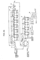
- Figs. 1A and 1B are block diagrams showing an entire construction of an embodiment of the present invention.
- An IC card 1 has an external terminal set 2. This external terminal set is used to electrically connect the IC card 1 to a terminal unit 30 when the card 1 is attached thereto.
- An external power, an external clock signal and an external reset signal are applied from the terminal unit 30 through respective terminals 2a, 2b and 2c of the external terminal set 2. Those external power, the external clock signal and the external reset signal are applied to a clock switching circuit 3.
- An internal oscillation circuit 4 is provided to generate an internal clock signal.
- the clock switching circuit 3 switches between an internal clock signal generated from the internal oscillation circuit 4 and the external clock signal inputted through the external terminal set 2 and applies the signal selected by the switching to an internal circuit 5.
- electric power is supplied from a battery 28 to the clock switching circuit 3, the internal oscillation circuit 4 and the internal circuit 5.
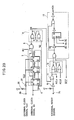
- Figs. 2A and 2B are specific definite electric circuit diagrams of the embodiment of the invention.
- a counter 17 is provided to output signals Q ⁇ 4 and Q ⁇ 5 for outputting a signal ⁇ p of a low (L) level from a NAND gate 18 and a signal ⁇ p of a high (H) level from an inverter 19 in response to the count of a predetermined number of pulses of an external clock signal f out .
- a switching circuit 20 is used to switch between an internal clock signal f in and the external clock signal f out in response to the signal ⁇ p, so that either clock signal is outputted as a system clock ⁇ to the internal circuit 5 shown in Fig. 1 and to a counter 21.
- the counter 21 is provided to output signals F1 to F4 for forming timing signals ACLR and ACL′ by means of gates 22 and 23 and a latch circuit 24.
- a counter circuit 7 is reset by an external clock signal f out , counts pulses of the internal clock signal f in and generates timing signals ARQ0 to ARQ2 for forming a signal AR.
- a latch circuit 12 is latched by an external reset signal and it is reset by a signal ACLR which attains H level after several cycles from the switching from the internal clock signal f in to the external clock signal f out .
- a synchronizing circuit 13 is provided to generate a signal ACL1 which synchronizes the output of the latch circuit 12 with clock signals ⁇ 3 and ⁇ 4 generated from the system clock ⁇ .
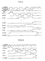
- Figs. 3, 4 and 5 are timing charts for explaining a definite operation of this embodiment.
- a power supply switch (not shown) provided in the IC card 1 is operated and then a power-on reset signal POR is applied to a reset input terminal of the counter 17 through an OR gate 16 shown in Fig. 2A, whereby the counter 17 is reset.
- the power-on reset signal POR is also applied to the counter 21 through an OR gate 25, whereby the counter 21 is reset.
- the outputs Q ⁇ 4 and Q ⁇ 5 of the counter 17 are lowered to L level and the respective outputs are supplied to the NAND gate 18.
- the signal ⁇ p outputted from the NAND gate 18 rises to H level and it is applied to one input terminal of the NAND gate 15. In consequence, this NAND gate 15 is opened. Further, the signal ⁇ p is inverted by the inverter 19 to the signal ⁇ p of L level, which is applied to the switching circuit 20. In response to this signal ⁇ p, the switching circuit 20 selects the internal clock signal f in and outputs this signal as the system clock pulse ⁇ to the internal circuit 5 shown in Fig. 1. Then, in response to the system clock pulse ⁇ , the internal circuit 5 carries out predetermined operation.
- the external power, the external clock signal f out and the external reset signal are applied from the terminal unit 30 to the external terminal set 2 of the card 1.
- the external reset signal of L level is inverted by the inverter 10 as shown in Fig. 2B and it is supplied as the signal ACL of H level to the OR circuit 11 as shown in (c) of Fig. 3.
- the OR circuit 11 outputs a signal ACLx of H level and in response to this signal, the latch circuit 12 is latched.
- the output of the latch circuit 12 is supplied to the synchronizing circuit 13 and the synchronizing circuit 13 synchronizes the clock pulses ⁇ 3 and ⁇ 4 with the output of the latch circuit 12 and outputs the signal ACL1 as shown in (j) of Fig. 3.
- This signal ACL1 is applied to one input terminal of the NAND gate 14.
- the NAND gate 14 is opened.
- the external clock signal f out as shown in Fig. (b) of Fig. 3 is applied to the other input terminal of the NAND gate 14.
- the external clock signal f out is applied to the NAND gate 15 through the NAND gate 14.
- the counter 17 is reset by the application of the signal ACLx outputted from the OR circuit 11 shown in Fig. 2B through the OR circuit 16 and, as shown in (f) and (g) of Fig. 3, the outputs Q ⁇ 4 and Q ⁇ 5 are respectively at L level.
- the signal ⁇ p outputted from the NAND gate 18 rises to H level as shown in (h) of Fig. 3, so that the NAND gate 15 is opened.
- the external clock signal f out is applied to the counter 17 through the NAND gate 15.
- the counter 17 starts counting pulses of the external clock signal f out .
- the signal ⁇ p of L level is inverted by the inverter 19 to H level and the signal of H level is applied to the switching circuit 20.
- the switching circuit 20 outputs the external clock signal f out as the system clock ⁇ to the internal circuit 5.
- the system clock ⁇ is applied to the counter 21, so that the counter 21 outputs the timing signals F1 to F3 as shown in (c), (d) and (e) of Fig. 5.
- the AND gate 22 outputs the signal ACLR of H level as shown in (k) of Fig. 3 and (f) of Fig. 5 and the latch circuit 12 shown in Fig. 2B is reset by the signal ACLR.
- the synchronizing circuit 13 When the latch circuit 12 is reset, the synchronizing circuit 13 outputs the signal ACL1 falling to L level as shown in (j) of Fig. 3.
- the NAND gate 14 is closed by the signal ACL1 and the external clock signal f out is not applied to the NAND 15.
- the signal ACL1 is used to enable the internal circuit 5. More specifically, the internal circuit 5 is initialized in a period of H level of the signal ACL1 and after the signal ACL1 falls to L level, the internal circuit 5 operates. Thus, as shown in (j) of Fig. 3, since the signal ACL1 falls to L level after several cycles from the switching from the internal clock signal f in to the external clock signal f out , the internal circuit 5 operates stably and erroneous operation can be prevented.
- the switching circuit 20 selects the internal clock signal f in and outputs it to the internal circuit 5.
- the IC card 1 is forcedly ejected from the terminal unit 30, switching occurs from the external clock signal f out to the internal clock signal f in and thereafter the signal ACL1 falls to L level, whereby the internal circuit 5 starts operation.
- the IC card when the IC card is attached to a terminal unit, pulses of the external clock signal supplied from the terminal unit are counted and, in response to counting of a predetermined number of pulses of the external clock signal, the external clock signal is selected and outputted in place of the internal clock signal. Accordingly, it can be correctly determined whether the IC card is operated in the form of a single body or in the form attached to any terminal unit.
Landscapes
- Engineering & Computer Science (AREA)
- Computer Hardware Design (AREA)
- Microelectronics & Electronic Packaging (AREA)
- Physics & Mathematics (AREA)
- General Physics & Mathematics (AREA)
- Theoretical Computer Science (AREA)
- Credit Cards Or The Like (AREA)
Applications Claiming Priority (2)
| Application Number | Priority Date | Filing Date | Title |
|---|---|---|---|
| JP63087996A JPH0610830B2 (ja) | 1988-04-09 | 1988-04-09 | Icカードのクロック信号切換装置 |
| JP87996/88 | 1988-04-09 |
Publications (3)
| Publication Number | Publication Date |
|---|---|
| EP0337684A2 true EP0337684A2 (de) | 1989-10-18 |
| EP0337684A3 EP0337684A3 (en) | 1990-12-27 |
| EP0337684B1 EP0337684B1 (de) | 1995-07-19 |
Family
ID=13930410
Family Applications (1)
| Application Number | Title | Priority Date | Filing Date |
|---|---|---|---|
| EP89303478A Expired - Lifetime EP0337684B1 (de) | 1988-04-09 | 1989-04-07 | Taktschaltgerät einer IC-Karte |
Country Status (4)
| Country | Link |
|---|---|
| US (1) | US4968899A (de) |
| EP (1) | EP0337684B1 (de) |
| JP (1) | JPH0610830B2 (de) |
| DE (1) | DE68923475T2 (de) |
Cited By (5)
| Publication number | Priority date | Publication date | Assignee | Title |
|---|---|---|---|---|
| GB2321744A (en) * | 1997-01-30 | 1998-08-05 | Motorola Inc | Portable data carrier and method for selecting an operating mode thereof |
| WO2001061638A1 (de) * | 2000-02-17 | 2001-08-23 | Orga Kartensysteme Gmbh | Chipkarte zur erfassung von messdaten |
| WO2001061639A1 (de) * | 2000-02-17 | 2001-08-23 | Orga Kartensysteme Gmbh | Chipkarte |
| WO2005109552A3 (de) * | 2004-04-30 | 2007-04-05 | Micronas Gmbh | Chip mit versorgungseinrichtung |
| DE102007039226A1 (de) | 2007-08-20 | 2009-02-26 | Giesecke & Devrient Gmbh | Echtzeitmessung auf einem portablen Datenträger |
Families Citing this family (11)
| Publication number | Priority date | Publication date | Assignee | Title |
|---|---|---|---|---|
| JP2723296B2 (ja) * | 1989-06-06 | 1998-03-09 | 株式会社東芝 | 携帯可能媒体 |
| US5313619A (en) * | 1991-05-16 | 1994-05-17 | Gerard J. Severance | External clock unit for a computer |
| US5155443A (en) * | 1990-12-19 | 1992-10-13 | Emhart Industries, Inc. | Machine for inspecting the wall thickness of glass containers |
| JPH04336308A (ja) * | 1991-05-13 | 1992-11-24 | Nec Corp | マイクロコンピュータ |
| US5483185A (en) * | 1994-06-09 | 1996-01-09 | Intel Corporation | Method and apparatus for dynamically switching between asynchronous signals without generating glitches |
| US5801561A (en) * | 1995-05-01 | 1998-09-01 | Intel Corporation | Power-on initializing circuit |
| JP3493096B2 (ja) * | 1996-06-07 | 2004-02-03 | 株式会社東芝 | 半導体集積回路、icカード、及びicカードシステム |
| DE10057477B4 (de) * | 2000-11-20 | 2007-05-24 | Sagem Orga Gmbh | Chipkarte |
| US7081780B2 (en) * | 2004-06-01 | 2006-07-25 | Randall Don Briggs | Reset circuitry for an integrated circuit |
| JP5166927B2 (ja) * | 2007-06-12 | 2013-03-21 | ルネサスエレクトロニクス株式会社 | 処理装置 |
| JP5742910B2 (ja) * | 2013-10-23 | 2015-07-01 | 大日本印刷株式会社 | Icチップ、icカード、及びicチップの動作方法 |
Family Cites Families (8)
| Publication number | Priority date | Publication date | Assignee | Title |
|---|---|---|---|---|
| GB2080585B (en) * | 1980-07-22 | 1984-07-04 | Tokyo Shibaura Electric Co | Semiconductor integrated circuit with reduced power consumption |
| JPS59193366A (ja) * | 1983-04-19 | 1984-11-01 | Ricoh Co Ltd | 交流電源の瞬断検知装置 |
| US4651277A (en) * | 1983-09-16 | 1987-03-17 | Sanyo Electric Co., Ltd. | Control system for a magnetic disk drive unit |
| EP0160163B1 (de) * | 1984-04-02 | 1988-06-08 | Mitsubishi Denki Kabushiki Kaisha | Steuersystem für eine frequenzvariable Stromversorgung |
| US4675539A (en) * | 1985-09-17 | 1987-06-23 | Codex Corporation | Backup power system |
| JPS62237592A (ja) * | 1986-04-08 | 1987-10-17 | Casio Comput Co Ltd | Icカ−ドにおけるクロツク切換方式 |
| EP0257648B1 (de) * | 1986-08-29 | 1992-07-15 | Kabushiki Kaisha Toshiba | Tragbarer Datenträger |
| US4850000A (en) * | 1987-11-05 | 1989-07-18 | Dallas Semiconductor Corporation | Gated shift register |
-
1988
- 1988-04-09 JP JP63087996A patent/JPH0610830B2/ja not_active Expired - Fee Related
-
1989
- 1989-04-07 EP EP89303478A patent/EP0337684B1/de not_active Expired - Lifetime
- 1989-04-07 DE DE68923475T patent/DE68923475T2/de not_active Expired - Lifetime
- 1989-04-07 US US07/334,566 patent/US4968899A/en not_active Expired - Lifetime
Cited By (8)
| Publication number | Priority date | Publication date | Assignee | Title |
|---|---|---|---|---|
| GB2321744A (en) * | 1997-01-30 | 1998-08-05 | Motorola Inc | Portable data carrier and method for selecting an operating mode thereof |
| GB2321744B (en) * | 1997-01-30 | 2000-05-17 | Motorola Inc | Portable data carrier and method for selecting operating mode thereof |
| US6138918A (en) * | 1997-01-30 | 2000-10-31 | Motorlola, Inc. | Portable data carrier and method for selecting operating mode thereof |
| WO2001061638A1 (de) * | 2000-02-17 | 2001-08-23 | Orga Kartensysteme Gmbh | Chipkarte zur erfassung von messdaten |
| WO2001061639A1 (de) * | 2000-02-17 | 2001-08-23 | Orga Kartensysteme Gmbh | Chipkarte |
| WO2005109552A3 (de) * | 2004-04-30 | 2007-04-05 | Micronas Gmbh | Chip mit versorgungseinrichtung |
| CN100552703C (zh) * | 2004-04-30 | 2009-10-21 | 迈克纳斯公司 | 具有供电装置的芯片 |
| DE102007039226A1 (de) | 2007-08-20 | 2009-02-26 | Giesecke & Devrient Gmbh | Echtzeitmessung auf einem portablen Datenträger |
Also Published As
| Publication number | Publication date |
|---|---|
| JPH0610830B2 (ja) | 1994-02-09 |
| JPH01259480A (ja) | 1989-10-17 |
| US4968899A (en) | 1990-11-06 |
| EP0337684B1 (de) | 1995-07-19 |
| DE68923475T2 (de) | 1996-02-15 |
| DE68923475D1 (de) | 1995-08-24 |
| EP0337684A3 (en) | 1990-12-27 |
Similar Documents
| Publication | Publication Date | Title |
|---|---|---|
| US4968899A (en) | Clock signal switching device of an IC Card | |
| KR920005171A (ko) | 테스트 모드 진입을 위한 연속적으로 클럭크된 호출 코드들을 가진 반도체 메모리 | |
| KR920005167A (ko) | 테스트 모드 진입을 위한 복수의 클럭킹을 가진 반도체 메모리 | |
| US5632680A (en) | Method and apparatus for controlling a computer game | |
| US4384326A (en) | Memory security circuit using the simultaneous occurance of two signals to enable the memory | |
| KR920003446B1 (ko) | 단일 출력단에서 정부 펄스를 발생하는 출력회로 | |
| US5479420A (en) | Clock fault monitoring circuit | |
| EP0158512A2 (de) | Rücksetzschaltung | |
| JPH0129093B2 (de) | ||
| EP0022458B1 (de) | Hierarchisches Datenverarbeitungssystem für eine Eingangskontrolle | |
| US3843893A (en) | Logical synchronization of test instruments | |
| EP3595174A2 (de) | Komparatorschaltung mit rückkopplung und verfahren zum betrieb | |
| US4198579A (en) | Input circuit for portable electronic devices | |
| JP3813994B2 (ja) | 差キャプチャ・タイマ | |
| US4365203A (en) | Multi-frequency clock generator with error-free frequency switching | |
| US4887071A (en) | Digital activity loss detector | |
| US5966034A (en) | Method and device for the filtering of a pulse signal | |
| US4010423A (en) | Multi-function remote control ic | |
| EP0005946A1 (de) | Periodenkomparator | |
| SU1049838A1 (ru) | Устройство контрол интегральных схем | |
| KR100365406B1 (ko) | 액정 디스플레이 컨트롤러의 자동 리셋 회로 | |
| EP0570143B1 (de) | Schnittstellenverfahren und -vorrichtung für serielles Datensignal | |
| JP2556038B2 (ja) | 混成集積回路 | |
| JPH0119545B2 (de) | ||
| KR910006702Y1 (ko) | 피포를 이용한 클럭소스의 안정도 측정회로 |
Legal Events
| Date | Code | Title | Description |
|---|---|---|---|
| PUAI | Public reference made under article 153(3) epc to a published international application that has entered the european phase |
Free format text: ORIGINAL CODE: 0009012 |
|
| AK | Designated contracting states |
Kind code of ref document: A2 Designated state(s): DE FR GB |
|
| PUAL | Search report despatched |
Free format text: ORIGINAL CODE: 0009013 |
|
| AK | Designated contracting states |
Kind code of ref document: A3 Designated state(s): DE FR GB |
|
| 17P | Request for examination filed |
Effective date: 19901214 |
|
| 17Q | First examination report despatched |
Effective date: 19930210 |
|
| GRAA | (expected) grant |
Free format text: ORIGINAL CODE: 0009210 |
|
| AK | Designated contracting states |
Kind code of ref document: B1 Designated state(s): DE FR GB |
|
| REF | Corresponds to: |
Ref document number: 68923475 Country of ref document: DE Date of ref document: 19950824 |
|
| ET | Fr: translation filed | ||
| PLBE | No opposition filed within time limit |
Free format text: ORIGINAL CODE: 0009261 |
|
| STAA | Information on the status of an ep patent application or granted ep patent |
Free format text: STATUS: NO OPPOSITION FILED WITHIN TIME LIMIT |
|
| 26N | No opposition filed | ||
| REG | Reference to a national code |
Ref country code: GB Ref legal event code: IF02 |
|
| PGFP | Annual fee paid to national office [announced via postgrant information from national office to epo] |
Ref country code: DE Payment date: 20080411 Year of fee payment: 20 Ref country code: FR Payment date: 20080312 Year of fee payment: 20 |
|
| PGFP | Annual fee paid to national office [announced via postgrant information from national office to epo] |
Ref country code: GB Payment date: 20080409 Year of fee payment: 20 |
|
| REG | Reference to a national code |
Ref country code: GB Ref legal event code: PE20 Expiry date: 20090406 |
|
| PG25 | Lapsed in a contracting state [announced via postgrant information from national office to epo] |
Ref country code: GB Free format text: LAPSE BECAUSE OF EXPIRATION OF PROTECTION Effective date: 20090406 |