EP0158512A2 - Rücksetzschaltung - Google Patents
Rücksetzschaltung Download PDFInfo
- Publication number
- EP0158512A2 EP0158512A2 EP85302372A EP85302372A EP0158512A2 EP 0158512 A2 EP0158512 A2 EP 0158512A2 EP 85302372 A EP85302372 A EP 85302372A EP 85302372 A EP85302372 A EP 85302372A EP 0158512 A2 EP0158512 A2 EP 0158512A2
- Authority
- EP
- European Patent Office
- Prior art keywords
- reset
- internal circuit
- circuit
- signal
- reset signal
- Prior art date
- Legal status (The legal status is an assumption and is not a legal conclusion. Google has not performed a legal analysis and makes no representation as to the accuracy of the status listed.)
- Ceased
Links
- 230000001052 transient effect Effects 0.000 claims abstract description 5
- 230000004044 response Effects 0.000 claims description 5
- 239000003990 capacitor Substances 0.000 abstract description 11
- 238000010586 diagram Methods 0.000 description 15
- 230000007704 transition Effects 0.000 description 10
- 230000007547 defect Effects 0.000 description 1
- 230000008034 disappearance Effects 0.000 description 1
- 230000006872 improvement Effects 0.000 description 1
- 230000002401 inhibitory effect Effects 0.000 description 1
- 230000007257 malfunction Effects 0.000 description 1
- 230000002093 peripheral effect Effects 0.000 description 1
Images


Classifications
-
- G—PHYSICS
- G06—COMPUTING; CALCULATING OR COUNTING
- G06F—ELECTRIC DIGITAL DATA PROCESSING
- G06F1/00—Details not covered by groups G06F3/00 - G06F13/00 and G06F21/00
- G06F1/24—Resetting means
Definitions
- the present invention relates to a reset circuit. More particularly, the present invention relates to an improvement of a reset circuit to be utilized in an electronic apparatus using a microcomputer.
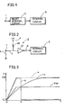
- Fig. 1 is a schematic block diagram showing structure of a conventional reset circuit
- Fig. 2 is a diagram showing a specific example of the conventional reset circuit shown in Fig. 1
- Fig. 3 is a waveform diagram showing operation of the Fig. 2 reset circuit at the time of turning on of the power source.
- a reset circuit as shown in Fig. 1 is employed for the purpose of resetting an internal logical circuit and the like.
- an input signal is supplied to a reset internal circuit 2 through an input terminal 1, a reset signal is generated from the reset internal circuit 2 so as to be supplied to an internal circuit 3.
- the internal circuit 3 is reset by this reset signal.
- the reset internal circuit 2 comprises as shown in Fig. 2, an inverter 21 for inverting the polarity of the input signal.
- An input terminal of the inverter 21 is connected to a DC power source (not shown)through a resistor 22.
- the input terminal 1 is connected in a reference potential, that is, a ground level for example, through a capacitor 4.
- the resistor 22 and the inverter 21 are contained in an integrated circuit, while the capacitor 4 is attached externally. Consequently, the reset internal circuit 2 shown in Fig. 1 contains the resistor 22 and the inverter 21.
- the reset circuit shown in Fig. 2 performs reset operation at the rise of DC voltage at the time of turning on of the power source. In the following, the reset operation will be described, with reference to Fig. 3.
- Fig. 3 shows waveforms concerning DC voltage a at the time of turning on of the power source, output voltage b of the inverter 21, voltage c in the reset input terminal 1 and transition voltage V TR1 of the inverter 21, the abscissa representing time t and the ordinate representing voltage V.
- the DC voltage a rises.
- the resistor 22 and the capacitor 4 constitute an RC series circuit
- the voltage c of the reset input terminal 1 increases with a time constant determined by the resistor 22 and the capacitor 4.
- the transition voltage V TR1 of the inverter 21 rises in proportion to the rise of the DC voltage a.
- the inverter 21 provides an "H” level when the input applied thereto is lower than the transition voltage V TR1 , and it provides an "L” level when the input applied thereto is higher than the transition voltage V TR1' Accordingly, in a period from t 0 to t 1 when the input voltage of the inverter 21, namely, the voltage c of the reset input terminal 1 is smaller than the transition voltage V TR1 , the output voltage b of the inverter 21 increases toward the "H" level so as to be maintained in the "H” level.
- the output voltage b of the inverter 21 descends to the "L" level to be maintained thereafter in the "L” level. Accordingly, the output voltage b of the inverter 21 has a pulse shape and the internal circuit 3 is reset in a period of the "H" level of the pulse shape.
- Fig. 4 is a schematic block diagram of a microcomputer circuit in which the conventional reset circuit shown in Figs. 1 and 2 is applied.
- an internal circuit 3 comprises a programmable counter 31, a programmable ROM 32, an arithmetic and logic unit (ALU) 33, a RAM 34, an input-output control circuit 35, an input-output port 36 and an external transistor 37.
- ALU arithmetic and logic unit
- RAM 34 RAM 34
- an input-output control circuit 35 an input-output port 36 and an external transistor 37.
- a reset signal is supplied from the inverter 21.
- the programmable counter 31 After the programmable counter 31 is reset in response to a reset signal, the programmable counter 31 counts clock pulses and supplies the output of the count to the programmable ROM 32 as an address signal.
- The, programmable ROM 32 reads out a program from a predetermined address according to the address signal to supply the program to the arithmetic and logic unit (ALU) 33.
- the ALU 33 performs processing operation based on the program and stores the data in the RAM 34.
- the input-output control circuit 35 is reset in response to a reset signal to control the external transistor 37 through the input-output port 36.
- the collector output of the external transistor 37 serves as a control signal for turning on and off the power source of a television receiver for example.
- the input-output port 36 shown in Fig. 4 serves as an input port and an output port and if this port serves as an output port at the time of turning on of the power source, an unfavorable influence might be exerted on an external system. More specifically stated, since the logical level of each circuit is not fixed till the ALU 33 executed the program of the programmable ROM 32 to set the internal state, the logical level is either the "H" level or the "L” level in case of the output state of the input-output port 36. If the input-output port 36 which is to operate as an input port is in the output state, an external signal output and an output of the microcomputer will be connected within the input-output port 36. If these outputs have different potentials, it is feared that a large current flows, causing damage to the microcomputer or the peripheral circuits.
- the input-output port 36 is controlled by the input-output control circuit 35 so that it serves as an input port in a period in which the output voltage of the inverter 21 is of the "H" level after the power source is turned on.
- the output voltage of the inverter 21 becomes the "L" level and in consequence the microcomputer performs an initializing routine set in the programmable ROM 32.
- the microcomputer sets the respective components in the initial state and sets the input-output port 36 to serve as an output port.
- the microcomputer advances to the main routine to repeat the operation in the main routine so that a normal state of operation of the system is maintained.
- a primary object of the present invention is to provide a reset circuit which will never makes erroneous operation due to external noise and other unfavorable influences.
- a reset signal for resetting an internal circuit is generated in response to an enabling signal applied to an input terminal. Then, it is determined whether the internal circuit is in a predetermined enabled state or not, and if the internal circuit is in the predetermined enabled state, application of the reset signal to the internal circuit is inhibited by reset inhibit means.
- a reset signal is generated based on transient phenomena at the time of turning on of the DC power source and the internal circuit generates a pulse signal indicating the predetermined enabled state so that the pulse signal is integrated. If the integrated pulse signal is within a predetermined level, it is determined that the internal circuit is in the enabled state and a decision signal is supplied to a gate circuit so that the gate is closed. Thus, the reset signal is inhibited from being supplied to the internal circuit.
- FIG. 5 is a schematic block diagram showing structure of an embodiment of the present invention.
- a reset circuit shown in Fig. 5 comprises a reset internal circuit 20 and a decision circuit 6 as is different from the above described reset circuit shown in Fig. 1.
- the reset internal circuit 20 receives an input signal from a reset input terminal 1 and generates a reset signal according to the input signal. The reset signal thus generated is supplied to an internal circuit 3.
- a microcomputer as shown in Fig. 4 or the like is employed.
- the internal circuit 3 When the internal circuit 3 is in a predetermined enabled state, it generates a signal indicating the enabled state and supplies the signal to the decision circuit 6.
- the decision circuit 6 receives the signal from the internal circuit 3 and determines whether the internal circuit 3 is in the predetermined enabled state. If the internal circuit 3 is in the predetermined enabled state, the decision circuit 6 supplies a reset inhibit signal to the reset internal circuit 20.
- the reset inhibit signal is supplied to the reset internal circuit 20, it functions to inhibit application of the reset signal to the internal circuit 3.
- Fig. 6 is a specific electrical circuit diagram of the embodiment shown in Fig. 5. Referring to Fig. 6, the structure of the embodiment will be described.
- the reset internal circuit 20 comprises an inverter 21, a resistor 22 and an AND gate 23.
- the inverter 21 and the resistor 22 are the same as those shown in Fig. 2.
- An output of the inverter 21 is supplied to one input terminal of the AND gate 23.
- a pulse signal a is generated.
- the pulse signal a is supplied to the decision circuit 6.
- the decision circuit 6 is structured by an integrating circuit comprising a resistor 61 and a capacitor 62 as well as by an inverter 63.
- the integrating circuit comprising the resistor 61 and the.
- the capacitor 62 serves to integrate the pulse signal a from the internal circuit 3 so as to provide a signal of a DC level.
- the signal thus integrated is supplied to the inverter 63.
- the inverter 63 it is determined whether the DC level of the pulse signal a integrated by the itegrating circuit comprising the resistor 61 and the capacitor 62 is higher than the transition voltage V TR1' If the D C level is lower than the transition voltage V TR1 , the inverter 63 provides a signal of the "H" level and if the DC level of the integrated signal is higher than the transition voltage V TR1 , it provides a reset inhibit signal c of the "L” level so that the signal c is supplied to the other input terminal of the above described AND gate 23. An output of the AND gate 23 is supplied to the internal circuit 3.
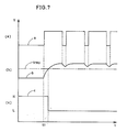
- Fig. 7 is a diagram showing waveforms of the respective components shown in Fig. 6. Referring to Fig. 7, the operation of the reset circuit shown in Fig. 6 will be described. Since the operation at the time of turning on of the power source takes almost the same waveforms as the previously described waveforms shown in Fig. 3, description of the operation will be made by partially utilizing Fig. 3. First, when the DC power source turns on at the time t 0 , the output of the inverter 21 becomes the "H" level as a result of the operation utilizing transient phenomena and after that, the output of the inverter 21 becomes the "L" level at the time t 1 . The operation performed hetherto is the same as in the conventional reset internal circuit shown in Fig. 3.
- the output a thereof takes a pulse shape as shown in Fig. 7(a).
- the pulse signal a from the internal circuit 3 is integrated by the integrating circuit comprising the resistor 61 and the capacitor 62 included in the decision circuit 6 and as shown in Fig. 7(b), the integrated output b becomes in a high level. If the circuit is preset such that the integrated output b is higher than the transition voltage V TR2 of the inverter 63, the integrated output b is applied to the inverter 63 as the "H" level. Then, the polarity of the integrated output b is inverted by the inverter 63 so that the output becomes the "L" level as shown in Fig. 7(c).
- the output c of the inverter 63 is maintained in the "L” level.
- the other input of the AND gate 23 is maintained in the "L” level during the operation of the internal circuit 3 and the gate is kept closed. Accordingly, if the voltage in the reset input terminal 1 becomes the “L” level because of mixing of noise and the output of the inverter 21 becomes in consequence the "H” level, the output of the AND gate 23 never becomes the "H” level. In other words, if a reset signal is applied to the internal circuit 3 during the operation due to noise, erroneous operation of the internal circuit 3 can be effectively prevented.
- the decision circuit 6 and the reset internal circuit 20 were shown in a specified manner, the present invention is not limited to those circuits. Other structure may be adopted as far as the necessary precision for the system is attained and the function of determining the enabled state of the internal circuit 3 and the function of inhibiting the reset thereof are performed.
Landscapes
- Engineering & Computer Science (AREA)
- Theoretical Computer Science (AREA)
- Physics & Mathematics (AREA)
- General Engineering & Computer Science (AREA)
- General Physics & Mathematics (AREA)
- Electronic Switches (AREA)
Applications Claiming Priority (2)
| Application Number | Priority Date | Filing Date | Title |
|---|---|---|---|
| JP59069406A JPS60212028A (ja) | 1984-04-05 | 1984-04-05 | リセツト回路 |
| JP69406/84 | 1984-04-05 |
Publications (2)
| Publication Number | Publication Date |
|---|---|
| EP0158512A2 true EP0158512A2 (de) | 1985-10-16 |
| EP0158512A3 EP0158512A3 (de) | 1987-11-19 |
Family
ID=13401686
Family Applications (1)
| Application Number | Title | Priority Date | Filing Date |
|---|---|---|---|
| EP85302372A Ceased EP0158512A3 (de) | 1984-04-05 | 1985-04-03 | Rücksetzschaltung |
Country Status (3)
| Country | Link |
|---|---|
| US (1) | US4670676A (de) |
| EP (1) | EP0158512A3 (de) |
| JP (1) | JPS60212028A (de) |
Cited By (4)
| Publication number | Priority date | Publication date | Assignee | Title |
|---|---|---|---|---|
| EP0323221A2 (de) * | 1987-12-28 | 1989-07-05 | Nec Corporation | Detektor für den augenblicklichen Spannungsabfall für Gleichstromquellen |
| AU630674B2 (en) * | 1989-03-23 | 1992-11-05 | Alcatel Australia Limited | Watchdog timer circuit |
| EP0665488A2 (de) * | 1994-01-27 | 1995-08-02 | Rockwell International Corporation | Schaltung zur Unterscheidung der Versorgung mit Rücksetzdetektion beim Einschalten |
| EP0825518A1 (de) * | 1996-08-20 | 1998-02-25 | Compaq Computer Corporation | PCI-Busbrückerücksetzschaltung |
Families Citing this family (19)
| Publication number | Priority date | Publication date | Assignee | Title |
|---|---|---|---|---|
| DE3510524A1 (de) * | 1985-03-22 | 1986-10-02 | Siemens AG, 1000 Berlin und 8000 München | Vorrichtung zur eigenueberwachung einer schaltungsanordnung mit einem mikrocomputer |
| US4803702A (en) * | 1986-08-05 | 1989-02-07 | Advanced Micro Devices, Inc. | Reset and synchronization interface circuit |
| JPH0797721B2 (ja) * | 1987-10-08 | 1995-10-18 | 原田工業株式会社 | 自動車用アンテナ制御装置 |
| US4860289A (en) * | 1987-10-19 | 1989-08-22 | John Fluke Mfg. Co., Inc. | Reset circuit for electrically isolated circuits communicating via uart |
| JPH01137853A (ja) * | 1987-11-25 | 1989-05-30 | Toshiba Corp | 通信制御システム |
| US5048017A (en) * | 1988-12-29 | 1991-09-10 | Breneman Brian H | Watchdog timer |
| JPH0312338U (de) * | 1989-06-20 | 1991-02-07 | ||
| US5148051A (en) * | 1990-12-14 | 1992-09-15 | Dallas Semiconductor Corporation | Power up circuit |
| FR2684206B1 (fr) * | 1991-11-25 | 1994-01-07 | Sgs Thomson Microelectronics Sa | Circuit de lecture de fusible de redondance pour memoire integree. |
| JPH07160666A (ja) * | 1993-12-10 | 1995-06-23 | Zexel Corp | マイクロコンピュータのリセット装置 |
| US5567993A (en) * | 1994-06-23 | 1996-10-22 | Dallas Semiconductor Corporation | Programmable power supply system and methods |
| US5537360A (en) * | 1994-09-16 | 1996-07-16 | Dallas Semiconductor Corporation | Programmable power supply systems and methods providing a write protected memory having multiple interface capability |
| DE69609530T2 (de) * | 1995-12-29 | 2001-03-29 | Advanced Micro Devices Inc | Rücksetzschaltung für eine batterie-getriebene integrierte schaltung und verfahren zum rücksetzen dieser integrierten schaltung |
| KR0174484B1 (ko) * | 1996-03-13 | 1999-04-01 | 김광호 | 고속 모드 변환 기능을 갖는 모뎀용 리셋장치 |
| JP3520662B2 (ja) * | 1996-04-09 | 2004-04-19 | 日産自動車株式会社 | 電子コントロールユニットの監視装置 |
| US5959926A (en) * | 1996-06-07 | 1999-09-28 | Dallas Semiconductor Corp. | Programmable power supply systems and methods providing a write protected memory having multiple interface capability |
| JP2001228936A (ja) * | 2000-02-18 | 2001-08-24 | Mitsubishi Electric Corp | 内部リセット信号生成回路を備えるマイクロコンピュータ |
| JP4294503B2 (ja) * | 2003-07-31 | 2009-07-15 | 富士通マイクロエレクトロニクス株式会社 | 動作モード制御回路、動作モード制御回路を含むマイクロコンピュータ及びそのマイクロコンピュータを利用した制御システム |
| JP4811640B2 (ja) * | 2005-08-04 | 2011-11-09 | 奥村遊機株式会社 | パチンコ機 |
Citations (2)
| Publication number | Priority date | Publication date | Assignee | Title |
|---|---|---|---|---|
| US4296338A (en) * | 1979-05-01 | 1981-10-20 | Motorola, Inc. | Power on and low voltage reset circuit |
| EP0096531A1 (de) * | 1982-06-09 | 1983-12-21 | Fujitsu Limited | Ein-Chip-Halbleitervorrichtung, die eine Versorgungsspannungsdetektorschaltung mit Rücksetzfunktion enthält |
Family Cites Families (11)
| Publication number | Priority date | Publication date | Assignee | Title |
|---|---|---|---|---|
| US3894247A (en) * | 1973-12-26 | 1975-07-08 | Rockwell International Corp | Circuit for initalizing logic following power turn on |
| JPS55150026A (en) * | 1979-05-09 | 1980-11-21 | Fujitsu Ltd | Power-on clearing circuit |
| US4367422A (en) * | 1980-10-01 | 1983-01-04 | General Electric Company | Power on restart circuit |
| DE3040326C1 (de) * | 1980-10-25 | 1981-10-08 | Eurosil GmbH, 8000 München | Mikroprozessor mit Ruecksetz-Schaltanordnung |
| JPS57155601A (en) * | 1981-03-20 | 1982-09-25 | Nippon Denso Co Ltd | Car safety device |
| DE3119117C2 (de) * | 1981-05-14 | 1993-10-21 | Bosch Gmbh Robert | Vorrichtung zum Rücksetzen von Recheneinrichtungen |
| US4410991A (en) * | 1981-06-03 | 1983-10-18 | Gte Laboratories Incorporated | Supervisory control apparatus |
| JPS58140649A (ja) * | 1982-02-16 | 1983-08-20 | Fujitsu Ltd | 電圧検出回路 |
| JPS58158726A (ja) * | 1982-03-12 | 1983-09-21 | Fuji Xerox Co Ltd | マイクロコンピユ−タ用制御装置 |
| JPS58201154A (ja) * | 1982-05-19 | 1983-11-22 | Nissan Motor Co Ltd | アンチスキッド制御装置用マイクロコンピュータのモード監視制御装置 |
| US4438357A (en) * | 1982-06-17 | 1984-03-20 | Baxter Travenol Laboratories, Inc. | Level sensitive reset circuit for digital logic |
-
1984
- 1984-04-05 JP JP59069406A patent/JPS60212028A/ja active Pending
-
1985
- 1985-01-15 US US06/691,762 patent/US4670676A/en not_active Expired - Fee Related
- 1985-04-03 EP EP85302372A patent/EP0158512A3/de not_active Ceased
Patent Citations (2)
| Publication number | Priority date | Publication date | Assignee | Title |
|---|---|---|---|---|
| US4296338A (en) * | 1979-05-01 | 1981-10-20 | Motorola, Inc. | Power on and low voltage reset circuit |
| EP0096531A1 (de) * | 1982-06-09 | 1983-12-21 | Fujitsu Limited | Ein-Chip-Halbleitervorrichtung, die eine Versorgungsspannungsdetektorschaltung mit Rücksetzfunktion enthält |
Non-Patent Citations (2)
| Title |
|---|
| IBM TECHNICAL DISCLOSURE BULLETIN, vol. 23, no. 7A, December 1980, page 2666, New York, US; J.W. FREEMAN: "Controlling trap interrupts" * |
| IBM TECHNICAL DISCLOSURE BULLETIN, vol. 24, no. 1A, June 1981, page 220, New York, US; D.C. Cole et al.: "Inhibiting reset of buffered log during I/O resets" * |
Cited By (7)
| Publication number | Priority date | Publication date | Assignee | Title |
|---|---|---|---|---|
| EP0323221A2 (de) * | 1987-12-28 | 1989-07-05 | Nec Corporation | Detektor für den augenblicklichen Spannungsabfall für Gleichstromquellen |
| EP0323221A3 (en) * | 1987-12-28 | 1990-09-26 | Nec Corporation | Instantaneous voltage drop detector for dc power source |
| AU630674B2 (en) * | 1989-03-23 | 1992-11-05 | Alcatel Australia Limited | Watchdog timer circuit |
| EP0665488A2 (de) * | 1994-01-27 | 1995-08-02 | Rockwell International Corporation | Schaltung zur Unterscheidung der Versorgung mit Rücksetzdetektion beim Einschalten |
| EP0665488A3 (de) * | 1994-01-27 | 1999-01-27 | Rockwell International Corporation | Schaltung zur Unterscheidung der Versorgung mit Rücksetzdetektion beim Einschalten |
| EP0825518A1 (de) * | 1996-08-20 | 1998-02-25 | Compaq Computer Corporation | PCI-Busbrückerücksetzschaltung |
| US5867676A (en) * | 1996-08-20 | 1999-02-02 | Compaq Computer Corp. | Reset circuit for a peripheral component interconnect bus |
Also Published As
| Publication number | Publication date |
|---|---|
| US4670676A (en) | 1987-06-02 |
| JPS60212028A (ja) | 1985-10-24 |
| EP0158512A3 (de) | 1987-11-19 |
Similar Documents
| Publication | Publication Date | Title |
|---|---|---|
| US4670676A (en) | Reset circuit | |
| US4766567A (en) | One-chip data processing device including low voltage detector | |
| EP0205163B1 (de) | Zeitüberwachungsschaltung geeignet für Gebrauch in Mikrorechner | |
| US4479191A (en) | Integrated circuit with interruptable oscillator circuit | |
| EP0096531B1 (de) | Ein-Chip-Halbleitervorrichtung, die eine Versorgungsspannungsdetektorschaltung mit Rücksetzfunktion enthält | |
| KR910001327B1 (ko) | Cmos 입 출력회로 | |
| US4558233A (en) | CMOS power-on reset pulse generating circuit with extended reset pulse duration | |
| US4148099A (en) | Memory device having a minimum number of pins | |
| US6297751B1 (en) | Low-voltage joystick port interface | |
| AU612090B2 (en) | Power source control apparatus | |
| US5349689A (en) | Apparatus for maintaining reset on microprocessor until after electrical chattering from connection of removable memory cartridge has ceased | |
| US5717907A (en) | Method and apparatus for generating a reset pulse responsive to a threshold voltage and to a system clock | |
| US4560889A (en) | Automatic clear circuit | |
| EP0388116A1 (de) | Zeitgeberschaltung | |
| US4737666A (en) | Integrated circuit semiconductor device with reduced power dissipation in a power-down mode | |
| CN110992866A (zh) | 显示面板的驱动电路和电子设备的逻辑电路 | |
| KR940011660B1 (ko) | 워치독 회로 | |
| JPH05143211A (ja) | 入力インタフエース回路 | |
| JP2563565B2 (ja) | マイクロコンピュータ用リセット制御回路 | |
| KR200299465Y1 (ko) | 마이크로프로세서의 파워 다운 웨이크 업 회로 | |
| JPH0556042B2 (de) | ||
| KR890003753Y1 (ko) | 마이콤의 오동작시 자동 리세트회로 | |
| JPH0224287Y2 (de) | ||
| KR930002026Y1 (ko) | 주변장치의 프로그램을 위한 리세트회로 | |
| JPS6120077B2 (de) |
Legal Events
| Date | Code | Title | Description |
|---|---|---|---|
| PUAI | Public reference made under article 153(3) epc to a published international application that has entered the european phase |
Free format text: ORIGINAL CODE: 0009012 |
|
| AK | Designated contracting states |
Designated state(s): DE FR GB |
|
| PUAL | Search report despatched |
Free format text: ORIGINAL CODE: 0009013 |
|
| AK | Designated contracting states |
Kind code of ref document: A3 Designated state(s): DE FR GB |
|
| 17P | Request for examination filed |
Effective date: 19880503 |
|
| 17Q | First examination report despatched |
Effective date: 19890823 |
|
| STAA | Information on the status of an ep patent application or granted ep patent |
Free format text: STATUS: THE APPLICATION HAS BEEN REFUSED |
|
| 18R | Application refused |
Effective date: 19910616 |
|
| RIN1 | Information on inventor provided before grant (corrected) |
Inventor name: NISHITANI, KAZUHARUC/O MITSUBISHI DENKI K.K. |