EP0337658A1 - Selektive Plattierung durch Abtragen mittels eines Lasers - Google Patents
Selektive Plattierung durch Abtragen mittels eines Lasers Download PDFInfo
- Publication number
- EP0337658A1 EP0337658A1 EP89303386A EP89303386A EP0337658A1 EP 0337658 A1 EP0337658 A1 EP 0337658A1 EP 89303386 A EP89303386 A EP 89303386A EP 89303386 A EP89303386 A EP 89303386A EP 0337658 A1 EP0337658 A1 EP 0337658A1
- Authority
- EP
- European Patent Office
- Prior art keywords
- resist
- substrate
- plating
- laser
- selective
- Prior art date
- Legal status (The legal status is an assumption and is not a legal conclusion. Google has not performed a legal analysis and makes no representation as to the accuracy of the status listed.)
- Granted
Links
Images
Classifications
-
- C—CHEMISTRY; METALLURGY
- C25—ELECTROLYTIC OR ELECTROPHORETIC PROCESSES; APPARATUS THEREFOR
- C25D—PROCESSES FOR THE ELECTROLYTIC OR ELECTROPHORETIC PRODUCTION OF COATINGS; ELECTROFORMING; APPARATUS THEREFOR
- C25D5/00—Electroplating characterised by the process; Pretreatment or after-treatment of workpieces
- C25D5/34—Pretreatment of metallic surfaces to be electroplated
-
- C—CHEMISTRY; METALLURGY
- C23—COATING METALLIC MATERIAL; COATING MATERIAL WITH METALLIC MATERIAL; CHEMICAL SURFACE TREATMENT; DIFFUSION TREATMENT OF METALLIC MATERIAL; COATING BY VACUUM EVAPORATION, BY SPUTTERING, BY ION IMPLANTATION OR BY CHEMICAL VAPOUR DEPOSITION, IN GENERAL; INHIBITING CORROSION OF METALLIC MATERIAL OR INCRUSTATION IN GENERAL
- C23C—COATING METALLIC MATERIAL; COATING MATERIAL WITH METALLIC MATERIAL; SURFACE TREATMENT OF METALLIC MATERIAL BY DIFFUSION INTO THE SURFACE, BY CHEMICAL CONVERSION OR SUBSTITUTION; COATING BY VACUUM EVAPORATION, BY SPUTTERING, BY ION IMPLANTATION OR BY CHEMICAL VAPOUR DEPOSITION, IN GENERAL
- C23C18/00—Chemical coating by decomposition of either liquid compounds or solutions of the coating forming compounds, without leaving reaction products of surface material in the coating; Contact plating
- C23C18/16—Chemical coating by decomposition of either liquid compounds or solutions of the coating forming compounds, without leaving reaction products of surface material in the coating; Contact plating by reduction or substitution, e.g. electroless plating
- C23C18/1601—Process or apparatus
- C23C18/1603—Process or apparatus coating on selected surface areas
- C23C18/1605—Process or apparatus coating on selected surface areas by masking
-
- C—CHEMISTRY; METALLURGY
- C23—COATING METALLIC MATERIAL; COATING MATERIAL WITH METALLIC MATERIAL; CHEMICAL SURFACE TREATMENT; DIFFUSION TREATMENT OF METALLIC MATERIAL; COATING BY VACUUM EVAPORATION, BY SPUTTERING, BY ION IMPLANTATION OR BY CHEMICAL VAPOUR DEPOSITION, IN GENERAL; INHIBITING CORROSION OF METALLIC MATERIAL OR INCRUSTATION IN GENERAL
- C23C—COATING METALLIC MATERIAL; COATING MATERIAL WITH METALLIC MATERIAL; SURFACE TREATMENT OF METALLIC MATERIAL BY DIFFUSION INTO THE SURFACE, BY CHEMICAL CONVERSION OR SUBSTITUTION; COATING BY VACUUM EVAPORATION, BY SPUTTERING, BY ION IMPLANTATION OR BY CHEMICAL VAPOUR DEPOSITION, IN GENERAL
- C23C18/00—Chemical coating by decomposition of either liquid compounds or solutions of the coating forming compounds, without leaving reaction products of surface material in the coating; Contact plating
- C23C18/16—Chemical coating by decomposition of either liquid compounds or solutions of the coating forming compounds, without leaving reaction products of surface material in the coating; Contact plating by reduction or substitution, e.g. electroless plating
- C23C18/1601—Process or apparatus
- C23C18/1603—Process or apparatus coating on selected surface areas
- C23C18/1607—Process or apparatus coating on selected surface areas by direct patterning
- C23C18/1608—Process or apparatus coating on selected surface areas by direct patterning from pretreatment step, i.e. selective pre-treatment
-
- C—CHEMISTRY; METALLURGY
- C23—COATING METALLIC MATERIAL; COATING MATERIAL WITH METALLIC MATERIAL; CHEMICAL SURFACE TREATMENT; DIFFUSION TREATMENT OF METALLIC MATERIAL; COATING BY VACUUM EVAPORATION, BY SPUTTERING, BY ION IMPLANTATION OR BY CHEMICAL VAPOUR DEPOSITION, IN GENERAL; INHIBITING CORROSION OF METALLIC MATERIAL OR INCRUSTATION IN GENERAL
- C23C—COATING METALLIC MATERIAL; COATING MATERIAL WITH METALLIC MATERIAL; SURFACE TREATMENT OF METALLIC MATERIAL BY DIFFUSION INTO THE SURFACE, BY CHEMICAL CONVERSION OR SUBSTITUTION; COATING BY VACUUM EVAPORATION, BY SPUTTERING, BY ION IMPLANTATION OR BY CHEMICAL VAPOUR DEPOSITION, IN GENERAL
- C23C18/00—Chemical coating by decomposition of either liquid compounds or solutions of the coating forming compounds, without leaving reaction products of surface material in the coating; Contact plating
- C23C18/16—Chemical coating by decomposition of either liquid compounds or solutions of the coating forming compounds, without leaving reaction products of surface material in the coating; Contact plating by reduction or substitution, e.g. electroless plating
- C23C18/1601—Process or apparatus
- C23C18/1603—Process or apparatus coating on selected surface areas
- C23C18/1607—Process or apparatus coating on selected surface areas by direct patterning
- C23C18/1612—Process or apparatus coating on selected surface areas by direct patterning through irradiation means
-
- C—CHEMISTRY; METALLURGY
- C23—COATING METALLIC MATERIAL; COATING MATERIAL WITH METALLIC MATERIAL; CHEMICAL SURFACE TREATMENT; DIFFUSION TREATMENT OF METALLIC MATERIAL; COATING BY VACUUM EVAPORATION, BY SPUTTERING, BY ION IMPLANTATION OR BY CHEMICAL VAPOUR DEPOSITION, IN GENERAL; INHIBITING CORROSION OF METALLIC MATERIAL OR INCRUSTATION IN GENERAL
- C23C—COATING METALLIC MATERIAL; COATING MATERIAL WITH METALLIC MATERIAL; SURFACE TREATMENT OF METALLIC MATERIAL BY DIFFUSION INTO THE SURFACE, BY CHEMICAL CONVERSION OR SUBSTITUTION; COATING BY VACUUM EVAPORATION, BY SPUTTERING, BY ION IMPLANTATION OR BY CHEMICAL VAPOUR DEPOSITION, IN GENERAL
- C23C18/00—Chemical coating by decomposition of either liquid compounds or solutions of the coating forming compounds, without leaving reaction products of surface material in the coating; Contact plating
- C23C18/16—Chemical coating by decomposition of either liquid compounds or solutions of the coating forming compounds, without leaving reaction products of surface material in the coating; Contact plating by reduction or substitution, e.g. electroless plating
- C23C18/1601—Process or apparatus
- C23C18/1633—Process of electroless plating
- C23C18/1635—Composition of the substrate
- C23C18/1637—Composition of the substrate metallic substrate
-
- C—CHEMISTRY; METALLURGY
- C23—COATING METALLIC MATERIAL; COATING MATERIAL WITH METALLIC MATERIAL; CHEMICAL SURFACE TREATMENT; DIFFUSION TREATMENT OF METALLIC MATERIAL; COATING BY VACUUM EVAPORATION, BY SPUTTERING, BY ION IMPLANTATION OR BY CHEMICAL VAPOUR DEPOSITION, IN GENERAL; INHIBITING CORROSION OF METALLIC MATERIAL OR INCRUSTATION IN GENERAL
- C23C—COATING METALLIC MATERIAL; COATING MATERIAL WITH METALLIC MATERIAL; SURFACE TREATMENT OF METALLIC MATERIAL BY DIFFUSION INTO THE SURFACE, BY CHEMICAL CONVERSION OR SUBSTITUTION; COATING BY VACUUM EVAPORATION, BY SPUTTERING, BY ION IMPLANTATION OR BY CHEMICAL VAPOUR DEPOSITION, IN GENERAL
- C23C18/00—Chemical coating by decomposition of either liquid compounds or solutions of the coating forming compounds, without leaving reaction products of surface material in the coating; Contact plating
- C23C18/16—Chemical coating by decomposition of either liquid compounds or solutions of the coating forming compounds, without leaving reaction products of surface material in the coating; Contact plating by reduction or substitution, e.g. electroless plating
- C23C18/18—Pretreatment of the material to be coated
- C23C18/1803—Pretreatment of the material to be coated of metallic material surfaces or of a non-specific material surfaces
- C23C18/1813—Pretreatment of the material to be coated of metallic material surfaces or of a non-specific material surfaces by radiant energy
- C23C18/182—Radiation, e.g. UV, laser
-
- C—CHEMISTRY; METALLURGY
- C23—COATING METALLIC MATERIAL; COATING MATERIAL WITH METALLIC MATERIAL; CHEMICAL SURFACE TREATMENT; DIFFUSION TREATMENT OF METALLIC MATERIAL; COATING BY VACUUM EVAPORATION, BY SPUTTERING, BY ION IMPLANTATION OR BY CHEMICAL VAPOUR DEPOSITION, IN GENERAL; INHIBITING CORROSION OF METALLIC MATERIAL OR INCRUSTATION IN GENERAL
- C23C—COATING METALLIC MATERIAL; COATING MATERIAL WITH METALLIC MATERIAL; SURFACE TREATMENT OF METALLIC MATERIAL BY DIFFUSION INTO THE SURFACE, BY CHEMICAL CONVERSION OR SUBSTITUTION; COATING BY VACUUM EVAPORATION, BY SPUTTERING, BY ION IMPLANTATION OR BY CHEMICAL VAPOUR DEPOSITION, IN GENERAL
- C23C18/00—Chemical coating by decomposition of either liquid compounds or solutions of the coating forming compounds, without leaving reaction products of surface material in the coating; Contact plating
- C23C18/54—Contact plating, i.e. electroless electrochemical plating
-
- C—CHEMISTRY; METALLURGY
- C25—ELECTROLYTIC OR ELECTROPHORETIC PROCESSES; APPARATUS THEREFOR
- C25D—PROCESSES FOR THE ELECTROLYTIC OR ELECTROPHORETIC PRODUCTION OF COATINGS; ELECTROFORMING; APPARATUS THEREFOR
- C25D5/00—Electroplating characterised by the process; Pretreatment or after-treatment of workpieces
- C25D5/02—Electroplating of selected surface areas
- C25D5/022—Electroplating of selected surface areas using masking means
-
- C—CHEMISTRY; METALLURGY
- C25—ELECTROLYTIC OR ELECTROPHORETIC PROCESSES; APPARATUS THEREFOR
- C25D—PROCESSES FOR THE ELECTROLYTIC OR ELECTROPHORETIC PRODUCTION OF COATINGS; ELECTROFORMING; APPARATUS THEREFOR
- C25D5/00—Electroplating characterised by the process; Pretreatment or after-treatment of workpieces
- C25D5/02—Electroplating of selected surface areas
- C25D5/024—Electroplating of selected surface areas using locally applied electromagnetic radiation, e.g. lasers
-
- H—ELECTRICITY
- H05—ELECTRIC TECHNIQUES NOT OTHERWISE PROVIDED FOR
- H05K—PRINTED CIRCUITS; CASINGS OR CONSTRUCTIONAL DETAILS OF ELECTRIC APPARATUS; MANUFACTURE OF ASSEMBLAGES OF ELECTRICAL COMPONENTS
- H05K3/00—Apparatus or processes for manufacturing printed circuits
- H05K3/22—Secondary treatment of printed circuits
- H05K3/24—Reinforcing the conductive pattern
- H05K3/243—Reinforcing the conductive pattern characterised by selective plating, e.g. for finish plating of pads
-
- H—ELECTRICITY
- H05—ELECTRIC TECHNIQUES NOT OTHERWISE PROVIDED FOR
- H05K—PRINTED CIRCUITS; CASINGS OR CONSTRUCTIONAL DETAILS OF ELECTRIC APPARATUS; MANUFACTURE OF ASSEMBLAGES OF ELECTRICAL COMPONENTS
- H05K2201/00—Indexing scheme relating to printed circuits covered by H05K1/00
- H05K2201/10—Details of components or other objects attached to or integrated in a printed circuit board
- H05K2201/10613—Details of electrical connections of non-printed components, e.g. special leads
- H05K2201/10742—Details of leads
- H05K2201/10886—Other details
- H05K2201/10924—Leads formed from a punched metal foil
-
- H—ELECTRICITY
- H05—ELECTRIC TECHNIQUES NOT OTHERWISE PROVIDED FOR
- H05K—PRINTED CIRCUITS; CASINGS OR CONSTRUCTIONAL DETAILS OF ELECTRIC APPARATUS; MANUFACTURE OF ASSEMBLAGES OF ELECTRICAL COMPONENTS
- H05K3/00—Apparatus or processes for manufacturing printed circuits
- H05K3/0011—Working of insulating substrates or insulating layers
- H05K3/0017—Etching of the substrate by chemical or physical means
- H05K3/0026—Etching of the substrate by chemical or physical means by laser ablation
- H05K3/0032—Etching of the substrate by chemical or physical means by laser ablation of organic insulating material
-
- Y—GENERAL TAGGING OF NEW TECHNOLOGICAL DEVELOPMENTS; GENERAL TAGGING OF CROSS-SECTIONAL TECHNOLOGIES SPANNING OVER SEVERAL SECTIONS OF THE IPC; TECHNICAL SUBJECTS COVERED BY FORMER USPC CROSS-REFERENCE ART COLLECTIONS [XRACs] AND DIGESTS
- Y10—TECHNICAL SUBJECTS COVERED BY FORMER USPC
- Y10S—TECHNICAL SUBJECTS COVERED BY FORMER USPC CROSS-REFERENCE ART COLLECTIONS [XRACs] AND DIGESTS
- Y10S430/00—Radiation imagery chemistry: process, composition, or product thereof
- Y10S430/146—Laser beam
Definitions
- This invention relates to a method for laser treating a resist covered metal substrate to effect the removal of such resist over an extended area of the substrate area, preferably by a single laser shot, on which said laser pulse is imaged.
- the present invention relates to a method to permit the selective plating of a metal substrate, such as an electrical contact.
- the selective plating thereof such as by plating with a precious metal, is achieved herein by selectively removing a plating resist covering said substrate.
- Such removal is accomplished by matching or coupling the laser wavelength, preferably one operating in the U.V. range, such as an excimer laser, with the plating resist and metal substrate.
- a preferred embodiment of this invention is the selective plating of electrical terminals.
- such terminals are stamped and formed from metal strip and are attached to a carrier strip which is useful for strip feeding the terminals through successive manufacturing operations.
- One necessary manufacturing operation involves plating; i.e., electroplating, the electrical contact surfaces of the strip fed terminals with precious metal or semi-precious metal, such as gold or alloys thereof.
- precious metal or semi-precious metal such as gold or alloys thereof.
- Such metals are characterized by good electrical conductivity and little or no formation of oxides that reduce said conductivity. Therefore these metals, when applied as plating, will improve conductivity of the terminals.
- the high cost of these metals has necessitated precision deposition on the contact surfaces of the terminals, and not on surfaces of the terminals on which plating is not necessary.
- the present invention achieves this result by a method not found nor reported on in the prior art.
- U.S. Patent No. 4,348,263 to Draper et al and directed to a process for surface melting of a substrate prior to plating teaches a method of making an electrical contact by the steps of applying a first protective layer to a substrate, subjecting said protective layer and a portion of said substrate to melting by means of an electron beam or laser prior to the deposition.
- a related work by Draper, published in the Gold Bulletin , 1986, 19, entitled “Laser Surface Alloying of Gold,” contains an illustrated showing on the mechanism of laser surface alloying by the use of focussed laser pulsing.
- the reason for the residual layer is believed to be a fundamental boundary condition on electromagnetic waves outside a metal surface. It is known that as a result of such condition, there is a decrease of the transverse electric field to small values as the metal surface is approached, thus ensuring insufficient direct heating of the polymer immediately adjoining the metal. This effect is further aggravated by the heat-sinking effect of the cold metal substrate surface underlying the polymer. To compensate, if a polymer is selected to have a very high absorption coefficient at the high wavelength of the laser to combat this effect, only a thin layer comparable to the optical absorption depth is removed with a single laser shot. As a consequence, multiple shots are required.
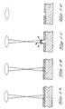
- This invention is directed to a method for the selective plating of a metal substrate on which a thin polymeric plating resist is first applied, followed by the selective removal of said resist to expose portions of said substrate to plating, and plating. More particularly, the method hereof includes the steps of selecting a laser wavelength which is strongly absorbed by the metal substrate, i.e.
- a polymer based plating resist having a low optical coefficient of absorption to a laser wavelength, typically between about 248 to 360 nm, curing said resist, preferably subjecting selective areas of said resist to a single excimer laser shot, having a wavelength between about 248 to 360 nm, to heat the metal substrate and thereby cause ablative removal of the resist over the selective areas of said substrate, and subjecting said exposed portions of said substrate to metal plating.
- the selective plating according to the practice of this invention is achieved by removing portions of the plating resist by directing a single excimer laser shot or optionally multiple shots, at the resist. By laser ablation, a selective portion of the resist is removed to expose a clean substrate suitable for plating.
- excimer lasers form a group of pulsed high-pressure gas lasers which emit various ultraviolet wavelengths, depending on the lasing medium, such as 193 nm, 248 nm, 308 nm and 351 nm.
- the lasing medium such as 193 nm, 248 nm, 308 nm and 351 nm.
- operating in the infrared region are such lasers whose laser sources are carbon dioxide (CO2), and neodymium doped yttrium-aluminum garnet (Nd:YAG).
- typical wavelengths for the three commercial laser units are as follows: Excimer 193, 248, 308, 351nm CO2 10,600nm ND:YAG 1,064nm
- Excimer 193, 248, 308, 351nm CO2 10,600nm ND:YAG 1,064nm The criticality of the proper selection of laser unit, by virtue of the precise wavelength range to which this invention relates, will become clearer from a further reading of these specifications.
- the plating resist selected to practice this invention must have a low optical absorption coefficient, e.g. with absorption coefficient preferably no greater than about 1000cm for a 3 micron film thickness.
- a suitable plating resist for use at laser wavelengths between, for instance about 300 to 360 nm, is a styrene acrylic copolymer, marketed under the designation WS5230, manufactured by Thiele-Engdahl.
- the optical absorption coefficient is wavelength related as illustrated in the following data of TABLE I.
- the optical absorption coefficient of a typical polymer resist is quite high, see Table I, such that all energy of the laser beam is absorbed in the outermost layer, i.e. 0.5 microns, of the resist. If the resist is greater than about 0.5 microns, then multiple laser shots are required. Thus, there is a critical window of wavelengths which must be achieved to successfuly ablate a plating resist in a single shot.
- both copper and nickel reveal reflectivity values within a 35 to 50% range for the lower wavelengths, values which are well suited to practice this invention.
- the metal substrate should reflect no more than about 70%, i.e. absorbing 30%. In such practice, it will be understood that the laser beam is primarily absorbed by the metal substrate which transmits energy to the overlying plating resist, primarily by conduction.
- an energy density level of at least about 0.90 J/cm2 is needed to achieve single shot ablation of the plating resist of 5.0 ⁇ in thickness.
- higher energy densities on the order of about 2.5 J/cm2, or higher, are required.
- This process thus achieves single-shot removal of films more than twenty times the greatest thickness per shot removed by conventional ablation, such as described earlier by Srinivasan and Cole, and their co-workers.
- the polymer can be removed without any readily detectable alteration of the metal.
- Nickel plated flat stock, and stamped electrical contacts were sprayed electrostatically with plating resists (WS5229 or WS5230), both of which have the same resin basis, an acrylic styrene co-polymer.
- the samples were dried in an infrared oven at about 275°F for one minute.
- the dried samples has a nominal thickness of 150 microinches. However, as noted previously, the resist coating thickness is not a significant process variable.
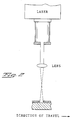
- the sprayed and dried samples were ablated by the excimer laser* in a setup shown in Figure 2.
- the ablated area was defined through an aperture and a lens.
- a transport mechanism was used to move the parts and ablate the parts continuously. Synchronization between the parts and the laser was obtained by adjusting the repetition rate of the laser and the transport speed, or by the use of an optical detector system.
- Immersion plating is very sensitive to the surface cleanliness. For example, the presence of a thin organic coating such as residual polymer, which may result from incomplete ablation, will inhibit the ion exchange between the gold bath and the nickel surfaces and cause non plating.
- Samples ablated by the parameters above were activated in an M629 bath, an activation solution that removes the surface oxide prior to gold plating, for 15 seconds and immerse plated in a Technic Oromerse "N", a gold plating solution, for 90 seconds at about 80°C. All samples were plated and indicated the absence of the residual polymer. The results were confirmed by ESCA studies of the surface.
- Electrolytic plating was used to obtain a thick nickel hardened gold plating for evaluation of the plating properties.
- plating substrates were first subjected to an activation bath. Thereafter, such substrates were electroplated in a bath having the following parameters: * gold concentration 2 tr. oz./gal * nickel concentration 2100 ppm * pH 4.6 - 4.8 * temperature 120 F * efficiency @ 40 ASF and 120 F 40 - 50% From such process, a gold deposit thickness of 30 ⁇ was achieved in a dwell time of from 45 to 60 seconds.
Landscapes
- Chemical & Material Sciences (AREA)
- Engineering & Computer Science (AREA)
- Materials Engineering (AREA)
- Chemical Kinetics & Catalysis (AREA)
- Organic Chemistry (AREA)
- Metallurgy (AREA)
- Mechanical Engineering (AREA)
- General Chemical & Material Sciences (AREA)
- Electrochemistry (AREA)
- Health & Medical Sciences (AREA)
- Physics & Mathematics (AREA)
- Toxicology (AREA)
- Optics & Photonics (AREA)
- Electromagnetism (AREA)
- Manufacturing & Machinery (AREA)
- Microelectronics & Electronic Packaging (AREA)
- Laser Beam Processing (AREA)
- Electroplating Methods And Accessories (AREA)
- Chemically Coating (AREA)
Applications Claiming Priority (2)
| Application Number | Priority Date | Filing Date | Title |
|---|---|---|---|
| US180417 | 1988-04-12 | ||
| US07/180,417 US4877644A (en) | 1988-04-12 | 1988-04-12 | Selective plating by laser ablation |
Publications (2)
| Publication Number | Publication Date |
|---|---|
| EP0337658A1 true EP0337658A1 (de) | 1989-10-18 |
| EP0337658B1 EP0337658B1 (de) | 1993-11-24 |
Family
ID=22660385
Family Applications (1)
| Application Number | Title | Priority Date | Filing Date |
|---|---|---|---|
| EP89303386A Expired - Lifetime EP0337658B1 (de) | 1988-04-12 | 1989-04-06 | Selektive Plattierung durch Abtragen mittels eines Lasers |
Country Status (4)
| Country | Link |
|---|---|
| US (1) | US4877644A (de) |
| EP (1) | EP0337658B1 (de) |
| JP (1) | JP2683696B2 (de) |
| DE (1) | DE68910864T2 (de) |
Cited By (5)
| Publication number | Priority date | Publication date | Assignee | Title |
|---|---|---|---|---|
| EP0459461B1 (de) * | 1990-05-31 | 1995-08-23 | Toshiba Tungaloy Co. Ltd. | Mehrfarbiges Produkt und Verfahren zur Herstellung desselben |
| EP1302563A1 (de) * | 2001-10-11 | 2003-04-16 | FRANZ Oberflächentechnik GmbH & Co KG | Erzeugung metallisch leitfähiger Oberflächenbereiche auf beschichteten Leichtmetalllegierungen |
| EP1409772B2 (de) † | 2001-07-20 | 2008-08-13 | Imo Ingo Müller E.K. | Verfahren zur selektiven galvanisierung eines bandartigen, metallischen trägermaterials |
| CN107904577A (zh) * | 2017-11-20 | 2018-04-13 | 北京理工大学 | 一种基于电子动态调控的浸润性可控的表面制备方法 |
| EP4048037A1 (de) * | 2021-02-19 | 2022-08-24 | Toyota Jidosha Kabushiki Kaisha | Verfahren zur herstellung einer leiterplatte |
Families Citing this family (52)
| Publication number | Priority date | Publication date | Assignee | Title |
|---|---|---|---|---|
| IL84255A (en) * | 1987-10-23 | 1993-02-21 | Galram Technology Ind Ltd | Process for removal of post- baked photoresist layer |
| JP2840098B2 (ja) * | 1988-02-05 | 1998-12-24 | レイケム・リミテッド | ポリマーのレーザー加工 |
| US5171709A (en) * | 1988-07-25 | 1992-12-15 | International Business Machines Corporation | Laser methods for circuit repair on integrated circuits and substrates |
| US5182230A (en) * | 1988-07-25 | 1993-01-26 | International Business Machines Corporation | Laser methods for circuit repair on integrated circuits and substrates |
| JP2862637B2 (ja) * | 1990-06-01 | 1999-03-03 | 株式会社東芝 | サーマルヘッドの製造方法 |
| US5182188A (en) * | 1990-06-29 | 1993-01-26 | General Electric Company | Method of developing a self-developing resist |
| US5147680A (en) * | 1990-11-13 | 1992-09-15 | Paul Slysh | Laser assisted masking process |
| US5259311A (en) * | 1992-07-15 | 1993-11-09 | Mark/Trece Inc. | Laser engraving of photopolymer printing plates |
| US5380474A (en) * | 1993-05-20 | 1995-01-10 | Sandia Corporation | Methods for patterned deposition on a substrate |
| US5403627A (en) * | 1993-06-04 | 1995-04-04 | Xerox Corporation | Process and apparatus for treating a photoreceptor coating |
| WO1995007152A1 (en) * | 1993-09-08 | 1995-03-16 | Uvtech Systems, Inc. | Surface processing |
| US5814156A (en) * | 1993-09-08 | 1998-09-29 | Uvtech Systems Inc. | Photoreactive surface cleaning |
| JP2951215B2 (ja) * | 1993-09-10 | 1999-09-20 | レイセオン・カンパニー | 位相マスクレーザによる微細なパターンの電子相互接続構造の製造方法 |
| US5424508A (en) * | 1994-01-06 | 1995-06-13 | Xerox Corporation | Laser ablation system |
| US5496985A (en) * | 1994-04-01 | 1996-03-05 | Xerox Corporation | Laser ablation nozzle |
| US5485935A (en) * | 1994-04-01 | 1996-01-23 | Xerox Corporation | Capture system employing diverter fluid nozzle |
| US5460284A (en) * | 1994-04-01 | 1995-10-24 | Xerox Corporation | Capture system employing annular fluid stream |
| US5562840A (en) * | 1995-01-23 | 1996-10-08 | Xerox Corporation | Substrate reclaim method |
| DE69631462D1 (de) * | 1995-11-27 | 2004-03-11 | Vlt Corp | Plattierung von permeablen Kernen |
| US5725706A (en) * | 1996-03-12 | 1998-03-10 | The Whitaker Corporation | Laser transfer deposition |
| US5887324A (en) * | 1996-08-30 | 1999-03-30 | The Whitaker Corporation | Electrical terminal with integral capacitive filter |
| SG76591A1 (en) * | 1999-02-27 | 2000-11-21 | Aem Tech Engineers Pte Ltd | Method for selective plating of a metal substrate using laser developed masking layer and apparatus for carrying out the method |
| DE19934584A1 (de) * | 1999-07-23 | 2001-01-25 | Inovan Stroebe | Verfahren zum Herstellen von Kontakten |
| GB2379324B (en) | 2000-06-01 | 2004-11-10 | Seagate Technology Llc | Magnetic recording head with dielectric layer |
| EP1253217A4 (de) * | 2000-07-06 | 2006-11-29 | Nat Inst Of Advanced Ind Scien | Vorbehandlungsverfahren von stromlos zu beschichtendes material |
| SG98017A1 (en) * | 2000-12-19 | 2003-08-20 | Inst Materials Research & Eng | Method of forming selective electronics plating on polymer surfaces |
| JP4521228B2 (ja) * | 2003-07-28 | 2010-08-11 | 正也 市村 | 光析出による金メッキ法及び金メッキ膜形成装置 |
| US7084014B2 (en) * | 2003-10-07 | 2006-08-01 | Endicott Interconnect Technologies, Inc. | Method of making circuitized substrate |
| GB0400982D0 (en) | 2004-01-16 | 2004-02-18 | Fujifilm Electronic Imaging | Method of forming a pattern on a substrate |
| US20050279453A1 (en) | 2004-06-17 | 2005-12-22 | Uvtech Systems, Inc. | System and methods for surface cleaning |
| US7600527B2 (en) | 2005-04-01 | 2009-10-13 | Fike Corporation | Reverse acting rupture disc with laser-defined electropolished line of weakness and method of forming the line of weakness |
| US7655972B2 (en) * | 2005-11-21 | 2010-02-02 | International Business Machines Corporation | Structure and method for MOSFET with reduced extension resistance |
| US20070235902A1 (en) * | 2006-03-31 | 2007-10-11 | 3M Innovative Properties Company | Microstructured tool and method of making same using laser ablation |
| US20070231541A1 (en) * | 2006-03-31 | 2007-10-04 | 3M Innovative Properties Company | Microstructured tool and method of making same using laser ablation |
| US8420978B2 (en) * | 2007-01-18 | 2013-04-16 | The Board Of Trustees Of The University Of Illinois | High throughput, low cost dual-mode patterning method for large area substrates |
| US8003300B2 (en) * | 2007-04-12 | 2011-08-23 | The Board Of Trustees Of The University Of Illinois | Methods for fabricating complex micro and nanoscale structures and electronic devices and components made by the same |
| US8652763B2 (en) * | 2007-07-16 | 2014-02-18 | The Board Of Trustees Of The University Of Illinois | Method for fabricating dual damascene profiles using sub pixel-voting lithography and devices made by same |
| US8546067B2 (en) * | 2008-03-21 | 2013-10-01 | The Board Of Trustees Of The University Of Illinois | Material assisted laser ablation |
| WO2009124180A2 (en) * | 2008-04-02 | 2009-10-08 | The Trustees Of Columbia University In The City Of New York | In situ plating and soldering of materials covered with a surface film |
| US8187795B2 (en) * | 2008-12-09 | 2012-05-29 | The Board Of Trustees Of The University Of Illinois | Patterning methods for stretchable structures |
| US8197037B2 (en) | 2009-12-15 | 2012-06-12 | Xerox Corporation | Method of removing thermoset polymer from piezoelectric transducers in a print head |
| US20120273261A1 (en) | 2010-10-20 | 2012-11-01 | Taiwan Green Point Enterprises Co., Ltd. | Circuit substrate having a circuit pattern and method for making the same |
| US8621749B2 (en) | 2010-03-12 | 2014-01-07 | Taiwan Green Point Enterprises Co., Ltd | Non-deleterious technique for creating continuous conductive circuits |
| US8952919B2 (en) | 2011-02-25 | 2015-02-10 | Taiwan Green Point Enterprises Co., Ltd. | Capacitive touch sensitive housing and method for making the same |
| ITVI20110122A1 (it) | 2011-05-13 | 2012-11-14 | St Microelectronics Srl | Metodo e apparato per la fabbricazione di lead frames |
| WO2017062423A1 (en) * | 2015-10-07 | 2017-04-13 | Corning Incorporated | Method of laser preparation of a coated substrate to be laser cut |
| DE102018218265A1 (de) * | 2018-10-25 | 2020-04-30 | MTU Aero Engines AG | Verfahren zum Herstellen einer Spitzenpanzerung an einer Laufschaufel einer Strömungsmaschine |
| DE102020107904B4 (de) | 2020-03-23 | 2022-04-28 | Lpkf Laser & Electronics Aktiengesellschaft | Verfahren zur Herstellung von Leiterbahnstrukturen auf einem nichtleitenden Trägersubstrat |
| CN112495451A (zh) * | 2020-11-24 | 2021-03-16 | 大连理工大学 | 一种利用激光加工技术制造固体催化剂的方法 |
| DE102020215293A1 (de) | 2020-12-03 | 2022-06-09 | Continental Teves Ag & Co. Ohg | Verfahren zur selektiven Nickelplattierung und Substrat |
| US11859092B2 (en) | 2021-03-26 | 2024-01-02 | Te Connectivity Solutions Gmbh | Printable non-curable thixotropic hot melt composition |
| US11859093B2 (en) | 2021-03-26 | 2024-01-02 | Te Connectivity Solutions Gmbh | Printable non-curable thixotropic hot melt composition |
Citations (3)
| Publication number | Priority date | Publication date | Assignee | Title |
|---|---|---|---|---|
| US4348263A (en) * | 1980-09-12 | 1982-09-07 | Western Electric Company, Inc. | Surface melting of a substrate prior to plating |
| EP0106977A2 (de) * | 1982-09-30 | 1984-05-02 | International Business Machines Corporation | Verfahren und Einrichtung für das elektrochemische Behandeln eines Substrats |
| EP0260514A1 (de) * | 1986-09-15 | 1988-03-23 | General Electric Company | Verfahren zur photoselektiven Metallisierung |
Family Cites Families (3)
| Publication number | Priority date | Publication date | Assignee | Title |
|---|---|---|---|---|
| US4414059A (en) * | 1982-12-09 | 1983-11-08 | International Business Machines Corporation | Far UV patterning of resist materials |
| US4671848A (en) * | 1984-12-17 | 1987-06-09 | General Laser, Inc. | Method for laser-induced removal of a surface coating |
| US4780177A (en) * | 1988-02-05 | 1988-10-25 | General Electric Company | Excimer laser patterning of a novel resist |
-
1988
- 1988-04-12 US US07/180,417 patent/US4877644A/en not_active Expired - Lifetime
-
1989
- 1989-04-06 EP EP89303386A patent/EP0337658B1/de not_active Expired - Lifetime
- 1989-04-06 DE DE68910864T patent/DE68910864T2/de not_active Expired - Fee Related
- 1989-04-12 JP JP1092806A patent/JP2683696B2/ja not_active Expired - Lifetime
Patent Citations (3)
| Publication number | Priority date | Publication date | Assignee | Title |
|---|---|---|---|---|
| US4348263A (en) * | 1980-09-12 | 1982-09-07 | Western Electric Company, Inc. | Surface melting of a substrate prior to plating |
| EP0106977A2 (de) * | 1982-09-30 | 1984-05-02 | International Business Machines Corporation | Verfahren und Einrichtung für das elektrochemische Behandeln eines Substrats |
| EP0260514A1 (de) * | 1986-09-15 | 1988-03-23 | General Electric Company | Verfahren zur photoselektiven Metallisierung |
Cited By (6)
| Publication number | Priority date | Publication date | Assignee | Title |
|---|---|---|---|---|
| EP0459461B1 (de) * | 1990-05-31 | 1995-08-23 | Toshiba Tungaloy Co. Ltd. | Mehrfarbiges Produkt und Verfahren zur Herstellung desselben |
| EP1409772B2 (de) † | 2001-07-20 | 2008-08-13 | Imo Ingo Müller E.K. | Verfahren zur selektiven galvanisierung eines bandartigen, metallischen trägermaterials |
| EP1302563A1 (de) * | 2001-10-11 | 2003-04-16 | FRANZ Oberflächentechnik GmbH & Co KG | Erzeugung metallisch leitfähiger Oberflächenbereiche auf beschichteten Leichtmetalllegierungen |
| WO2003033772A1 (de) * | 2001-10-11 | 2003-04-24 | Franz Oberflächentechnik Gmbh & Co. Kg | Erzeugung metallisch leitfähiger oberflächenbereiche auf beschichteten leichtmetalllegierungen |
| CN107904577A (zh) * | 2017-11-20 | 2018-04-13 | 北京理工大学 | 一种基于电子动态调控的浸润性可控的表面制备方法 |
| EP4048037A1 (de) * | 2021-02-19 | 2022-08-24 | Toyota Jidosha Kabushiki Kaisha | Verfahren zur herstellung einer leiterplatte |
Also Published As
| Publication number | Publication date |
|---|---|
| DE68910864D1 (de) | 1994-01-05 |
| JP2683696B2 (ja) | 1997-12-03 |
| US4877644A (en) | 1989-10-31 |
| EP0337658B1 (de) | 1993-11-24 |
| JPH0211773A (ja) | 1990-01-16 |
| DE68910864T2 (de) | 1994-06-01 |
Similar Documents
| Publication | Publication Date | Title |
|---|---|---|
| EP0337658B1 (de) | Selektive Plattierung durch Abtragen mittels eines Lasers | |
| US4904498A (en) | Method for controlling an oxide layer metallic substrates by laser | |
| US4898650A (en) | Laser cleaning of metal stock | |
| EP0787219B1 (de) | Verfahren zum beschichten von durchgangslöchern mit hilfe eines lasers | |
| US5292559A (en) | Laser transfer process | |
| US4832798A (en) | Method and apparatus for plating composite | |
| US4495255A (en) | Laser surface alloying | |
| US4348263A (en) | Surface melting of a substrate prior to plating | |
| Koren et al. | Particulates reduction in laser‐ablated YBa2Cu3O7− δ thin films by laser‐induced plume heating | |
| US5182230A (en) | Laser methods for circuit repair on integrated circuits and substrates | |
| CA2061296A1 (en) | Method for metallizing surfaces by means of metal powders | |
| US5127998A (en) | Area-selective metallization process | |
| EP1155168B1 (de) | Verfahren und vorrichtung zur selektiven plattierung eines metallischen trägers mit mittels eines lasers abgetragenen maskierungsschicht | |
| US4898648A (en) | Method for providing a strengthened conductive circuit pattern | |
| US5246745A (en) | Laser-induced chemical vapor deposition of thin-film conductors | |
| US5725706A (en) | Laser transfer deposition | |
| EP0366259A2 (de) | Verfahren zum Untereinanderverbinden von elektrischen Dünnschichtkreisen | |
| US5830376A (en) | Topographical selective patterns | |
| EP0557952B1 (de) | Beschichtungverfahren und damit hergestellte zylindrische Spule | |
| US4909895A (en) | System and method for providing a conductive circuit pattern utilizing thermal oxidation | |
| Kántor et al. | Dynamics of long‐pulse laser transfer of micrometer‐sized metal patterns as followed by time‐resolved measurements of reflectivity and transmittance | |
| US5171709A (en) | Laser methods for circuit repair on integrated circuits and substrates | |
| US5230965A (en) | High density interconnect with electroplated conductors | |
| Morita et al. | Direct formation of conductor films by laser sublimating of ceramics | |
| JP2613935B2 (ja) | セラミック回路基板の製造方法 |
Legal Events
| Date | Code | Title | Description |
|---|---|---|---|
| PUAI | Public reference made under article 153(3) epc to a published international application that has entered the european phase |
Free format text: ORIGINAL CODE: 0009012 |
|
| AK | Designated contracting states |
Kind code of ref document: A1 Designated state(s): DE GB NL |
|
| RAP1 | Party data changed (applicant data changed or rights of an application transferred) |
Owner name: AMP INCORPORATED |
|
| 17P | Request for examination filed |
Effective date: 19900405 |
|
| 17Q | First examination report despatched |
Effective date: 19920421 |
|
| RAP1 | Party data changed (applicant data changed or rights of an application transferred) |
Owner name: THE WHITAKER CORPORATION |
|
| GRAA | (expected) grant |
Free format text: ORIGINAL CODE: 0009210 |
|
| AK | Designated contracting states |
Kind code of ref document: B1 Designated state(s): DE GB NL |
|
| REF | Corresponds to: |
Ref document number: 68910864 Country of ref document: DE Date of ref document: 19940105 |
|
| PLBE | No opposition filed within time limit |
Free format text: ORIGINAL CODE: 0009261 |
|
| STAA | Information on the status of an ep patent application or granted ep patent |
Free format text: STATUS: NO OPPOSITION FILED WITHIN TIME LIMIT |
|
| 26N | No opposition filed | ||
| PGFP | Annual fee paid to national office [announced via postgrant information from national office to epo] |
Ref country code: GB Payment date: 19990315 Year of fee payment: 11 |
|
| PGFP | Annual fee paid to national office [announced via postgrant information from national office to epo] |
Ref country code: NL Payment date: 19990322 Year of fee payment: 11 |
|
| PGFP | Annual fee paid to national office [announced via postgrant information from national office to epo] |
Ref country code: DE Payment date: 19990430 Year of fee payment: 11 |
|
| PG25 | Lapsed in a contracting state [announced via postgrant information from national office to epo] |
Ref country code: GB Free format text: LAPSE BECAUSE OF NON-PAYMENT OF DUE FEES Effective date: 20000406 |
|
| PG25 | Lapsed in a contracting state [announced via postgrant information from national office to epo] |
Ref country code: NL Free format text: LAPSE BECAUSE OF NON-PAYMENT OF DUE FEES Effective date: 20001101 |
|
| GBPC | Gb: european patent ceased through non-payment of renewal fee |
Effective date: 20000406 |
|
| NLV4 | Nl: lapsed or anulled due to non-payment of the annual fee |
Effective date: 20001101 |
|
| PG25 | Lapsed in a contracting state [announced via postgrant information from national office to epo] |
Ref country code: DE Free format text: LAPSE BECAUSE OF NON-PAYMENT OF DUE FEES Effective date: 20010201 |