EP0332889B1 - Verfahren zum Aufbau einer Leiterplatten-Anordnung von hoher Leistungsfähigkeit - Google Patents
Verfahren zum Aufbau einer Leiterplatten-Anordnung von hoher Leistungsfähigkeit Download PDFInfo
- Publication number
- EP0332889B1 EP0332889B1 EP89103031A EP89103031A EP0332889B1 EP 0332889 B1 EP0332889 B1 EP 0332889B1 EP 89103031 A EP89103031 A EP 89103031A EP 89103031 A EP89103031 A EP 89103031A EP 0332889 B1 EP0332889 B1 EP 0332889B1
- Authority
- EP
- European Patent Office
- Prior art keywords
- sub
- assembly
- circuit board
- constructing
- printed circuit
- Prior art date
- Legal status (The legal status is an assumption and is not a legal conclusion. Google has not performed a legal analysis and makes no representation as to the accuracy of the status listed.)
- Expired - Lifetime
Links
- 238000000034 method Methods 0.000 title claims description 27
- 238000000429 assembly Methods 0.000 claims description 28
- 238000010276 construction Methods 0.000 claims description 17
- 238000010030 laminating Methods 0.000 claims description 12
- 238000004519 manufacturing process Methods 0.000 claims description 3
- 239000003822 epoxy resin Substances 0.000 claims description 2
- 229920000647 polyepoxide Polymers 0.000 claims description 2
- 239000002131 composite material Substances 0.000 claims 4
- RYGMFSIKBFXOCR-UHFFFAOYSA-N Copper Chemical compound [Cu] RYGMFSIKBFXOCR-UHFFFAOYSA-N 0.000 description 6
- 229910052802 copper Inorganic materials 0.000 description 6
- 239000010949 copper Substances 0.000 description 6
- 230000008901 benefit Effects 0.000 description 5
- 239000000463 material Substances 0.000 description 5
- 230000000712 assembly Effects 0.000 description 3
- 230000002950 deficient Effects 0.000 description 2
- 239000003989 dielectric material Substances 0.000 description 2
- 125000000951 phenoxy group Chemical group [H]C1=C([H])C([H])=C(O*)C([H])=C1[H] 0.000 description 2
- 239000013034 phenoxy resin Substances 0.000 description 2
- 229920006287 phenoxy resin Polymers 0.000 description 2
- 239000000654 additive Substances 0.000 description 1
- 230000000996 additive effect Effects 0.000 description 1
- 230000005540 biological transmission Effects 0.000 description 1
- 238000004891 communication Methods 0.000 description 1
- 239000004020 conductor Substances 0.000 description 1
- 238000005530 etching Methods 0.000 description 1
- 230000010354 integration Effects 0.000 description 1
- 238000003475 lamination Methods 0.000 description 1
- 238000007747 plating Methods 0.000 description 1
- 229920003217 poly(methylsilsesquioxane) Polymers 0.000 description 1
- 239000002699 waste material Substances 0.000 description 1
Images
Classifications
-
- H—ELECTRICITY
- H01—ELECTRIC ELEMENTS
- H01P—WAVEGUIDES; RESONATORS, LINES, OR OTHER DEVICES OF THE WAVEGUIDE TYPE
- H01P3/00—Waveguides; Transmission lines of the waveguide type
- H01P3/02—Waveguides; Transmission lines of the waveguide type with two longitudinal conductors
- H01P3/08—Microstrips; Strip lines
- H01P3/088—Stacked transmission lines
-
- H—ELECTRICITY
- H05—ELECTRIC TECHNIQUES NOT OTHERWISE PROVIDED FOR
- H05K—PRINTED CIRCUITS; CASINGS OR CONSTRUCTIONAL DETAILS OF ELECTRIC APPARATUS; MANUFACTURE OF ASSEMBLAGES OF ELECTRICAL COMPONENTS
- H05K3/00—Apparatus or processes for manufacturing printed circuits
- H05K3/44—Manufacturing insulated metal core circuits or other insulated electrically conductive core circuits
- H05K3/445—Manufacturing insulated metal core circuits or other insulated electrically conductive core circuits having insulated holes or insulated via connections through the metal core
-
- H—ELECTRICITY
- H05—ELECTRIC TECHNIQUES NOT OTHERWISE PROVIDED FOR
- H05K—PRINTED CIRCUITS; CASINGS OR CONSTRUCTIONAL DETAILS OF ELECTRIC APPARATUS; MANUFACTURE OF ASSEMBLAGES OF ELECTRICAL COMPONENTS
- H05K3/00—Apparatus or processes for manufacturing printed circuits
- H05K3/46—Manufacturing multilayer circuits
- H05K3/4611—Manufacturing multilayer circuits by laminating two or more circuit boards
- H05K3/4623—Manufacturing multilayer circuits by laminating two or more circuit boards the circuit boards having internal via connections between two or more circuit layers before lamination, e.g. double-sided circuit boards
-
- H—ELECTRICITY
- H05—ELECTRIC TECHNIQUES NOT OTHERWISE PROVIDED FOR
- H05K—PRINTED CIRCUITS; CASINGS OR CONSTRUCTIONAL DETAILS OF ELECTRIC APPARATUS; MANUFACTURE OF ASSEMBLAGES OF ELECTRICAL COMPONENTS
- H05K1/00—Printed circuits
- H05K1/02—Details
- H05K1/0213—Electrical arrangements not otherwise provided for
- H05K1/0237—High frequency adaptations
-
- H—ELECTRICITY
- H05—ELECTRIC TECHNIQUES NOT OTHERWISE PROVIDED FOR
- H05K—PRINTED CIRCUITS; CASINGS OR CONSTRUCTIONAL DETAILS OF ELECTRIC APPARATUS; MANUFACTURE OF ASSEMBLAGES OF ELECTRICAL COMPONENTS
- H05K2201/00—Indexing scheme relating to printed circuits covered by H05K1/00
- H05K2201/09—Shape and layout
- H05K2201/09209—Shape and layout details of conductors
- H05K2201/0929—Conductive planes
- H05K2201/09327—Special sequence of power, ground and signal layers in multilayer PCB
-
- H—ELECTRICITY
- H05—ELECTRIC TECHNIQUES NOT OTHERWISE PROVIDED FOR
- H05K—PRINTED CIRCUITS; CASINGS OR CONSTRUCTIONAL DETAILS OF ELECTRIC APPARATUS; MANUFACTURE OF ASSEMBLAGES OF ELECTRICAL COMPONENTS
- H05K2201/00—Indexing scheme relating to printed circuits covered by H05K1/00
- H05K2201/09—Shape and layout
- H05K2201/09209—Shape and layout details of conductors
- H05K2201/095—Conductive through-holes or vias
- H05K2201/09536—Buried plated through-holes, i.e. plated through-holes formed in a core before lamination
-
- H—ELECTRICITY
- H05—ELECTRIC TECHNIQUES NOT OTHERWISE PROVIDED FOR
- H05K—PRINTED CIRCUITS; CASINGS OR CONSTRUCTIONAL DETAILS OF ELECTRIC APPARATUS; MANUFACTURE OF ASSEMBLAGES OF ELECTRICAL COMPONENTS
- H05K2203/00—Indexing scheme relating to apparatus or processes for manufacturing printed circuits covered by H05K3/00
- H05K2203/06—Lamination
- H05K2203/061—Lamination of previously made multilayered subassemblies
-
- H—ELECTRICITY
- H05—ELECTRIC TECHNIQUES NOT OTHERWISE PROVIDED FOR
- H05K—PRINTED CIRCUITS; CASINGS OR CONSTRUCTIONAL DETAILS OF ELECTRIC APPARATUS; MANUFACTURE OF ASSEMBLAGES OF ELECTRICAL COMPONENTS
- H05K3/00—Apparatus or processes for manufacturing printed circuits
- H05K3/40—Forming printed elements for providing electric connections to or between printed circuits
- H05K3/42—Plated through-holes or plated via connections
- H05K3/425—Plated through-holes or plated via connections characterised by the sequence of steps for plating the through-holes or via connections in relation to the conductive pattern
- H05K3/427—Plated through-holes or plated via connections characterised by the sequence of steps for plating the through-holes or via connections in relation to the conductive pattern initial plating of through-holes in metal-clad substrates
-
- H—ELECTRICITY
- H05—ELECTRIC TECHNIQUES NOT OTHERWISE PROVIDED FOR
- H05K—PRINTED CIRCUITS; CASINGS OR CONSTRUCTIONAL DETAILS OF ELECTRIC APPARATUS; MANUFACTURE OF ASSEMBLAGES OF ELECTRICAL COMPONENTS
- H05K3/00—Apparatus or processes for manufacturing printed circuits
- H05K3/46—Manufacturing multilayer circuits
- H05K3/4611—Manufacturing multilayer circuits by laminating two or more circuit boards
- H05K3/4641—Manufacturing multilayer circuits by laminating two or more circuit boards having integrally laminated metal sheets or special power cores
-
- Y—GENERAL TAGGING OF NEW TECHNOLOGICAL DEVELOPMENTS; GENERAL TAGGING OF CROSS-SECTIONAL TECHNOLOGIES SPANNING OVER SEVERAL SECTIONS OF THE IPC; TECHNICAL SUBJECTS COVERED BY FORMER USPC CROSS-REFERENCE ART COLLECTIONS [XRACs] AND DIGESTS
- Y10—TECHNICAL SUBJECTS COVERED BY FORMER USPC
- Y10T—TECHNICAL SUBJECTS COVERED BY FORMER US CLASSIFICATION
- Y10T29/00—Metal working
- Y10T29/49—Method of mechanical manufacture
- Y10T29/49002—Electrical device making
- Y10T29/49117—Conductor or circuit manufacturing
- Y10T29/49124—On flat or curved insulated base, e.g., printed circuit, etc.
- Y10T29/49126—Assembling bases
Definitions
- the invention relates to a method of constructing a high performance printed circuit board assembly.
- High density printed circuit boards are generally constructed with several electrically conductive layers separated by dielectric layers. Some of the conductive layers are used to supply power and ground voltages. The remaining conductive layers are patterned for electrical signal interconnections among integrated circuit chips. Layer-to-layer interconnections are achieved by means of through-holes plated with electrically conductive material. In high density printed circuit boards it has been normal practice to provide interconnections between adjacent conducting layers, which interconnections are commonly known as "vias".
- circuit board construction has been useful in transmitting high frequency signals, and relies upon alternating dielectric mediums to achieve its many benefits.
- triplate construction has several drawbacks: (1) it is not a true triplate configuration in which X-Y signal planes are disposed about a conductive power or reference plane; (2) there is no teaching in the above-mentioned patent how vias can be fabricated between individual signal planes embedded as a core within the multi-laminated board structure; (3) if an electrical short should develop within any one of the cores of the assembly, the whole assembly must be discarded. Such electrical short circuits occur with greater prevalence in high performance circuit boards as layers become thinner and signal line density is increased.
- the invention as claimed is intended to remedy these drawbacks. It solves the problem of constructing high performance printed circuit board assemblies comprising at least two laminated circuitized power plane sub-assemblies.
- the circuitized power plane sub-assemblies are modular in that they are fabricated in a prior assembly process, and then laminated to other assembly elements as a finished core unit.
- each modular unit can be tested for electrical integrity prior to its integration into the final assembly.
- Defective circuit board sub-assemblies can be discarded rather than having to discard the completed assembly, as with present techniques.
- the invention thus provides less waste, and improves reliability.
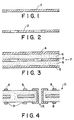
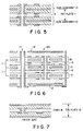
- the assembly of the invention is of true triplate construction, consisting of two laminated sub-assemblies characterized by spaced-apart X-Y signal planes disposed about an internal power plane. Vias run through the core where necessary to provide communication between the X and Y signal planes.
- the triplate core is prefabricated as follows:
- the final circuit board assembly will be comprised of a number of laminated sub-assemblies.
- Plated vias are fabricated in the sub-assemblies where necessary.
- Still another advantage of the modular technique of the invention is provided by the greater choice of laminating materials. For example, it is intended to reduce the overall dielectric character of the final assembly by laminating the sub-assemblies together using bonding films or a brominated phenoxy resin, rather than a glass resin.
Landscapes
- Engineering & Computer Science (AREA)
- Manufacturing & Machinery (AREA)
- Microelectronics & Electronic Packaging (AREA)
- Production Of Multi-Layered Print Wiring Board (AREA)
- Combinations Of Printed Boards (AREA)
Claims (10)
- Verfahren zum Aufbau einer Leiterplatten-Anordnung von hoher Leistungsfähigkeit mit Hilfe einer modularen Aufbaumethode, das die folgenden Schritte umfaßt:(a) das Anfertigen einer Reihe von Unterbaugruppen (10) mit Schaltkreise enthaltenden Stromversorgungsebenen, wobei jede entsprechende Unterbaugruppe eine Signalebene (4, 5) umfaßt, die auf gegenüberliegenden Seiten einer inneren Stromversorgungsebene (2) angeordnet sind und elektrisch dort, wo dies notwendig ist, durch beschichtete Durchverbindungen (13) verbunden sind; und(b) das Zusammenlaminieren von mindestens zwei Unterbaugruppen zur Bildung eines Dreiplatten-Konstruktions-Schichtkörpers (11); und(c) das Aufbauen einer Leiterplatten-Anordnung (20) durch das Herstellen einer mehrschichtigen Struktur mit Hilfe des Schichtkörpers.
- Verfahren zum Aufbau einer Leiterplatten-Anordnung von hoher Leistungsfähigkeit nach Anspruch 1, das im weiteren folgenden Schritt umfaßt:
(d) das Prüfen jeder entsprechenden Unterbaugruppe (10) auf elektrische Intaktheit vor dem Laminierungsschritt (b). - Verfahren zum Aufbau einer Leiterplatten-Anordnung hoher Leistungsfähigkeit nach Anspruch 1, bei dem die Herstellung jeder Unterbaugruppe von Schritt (a) im weiteren folgende Schritte umfaßt:(I) das Perforieren einer ersten leitenden Schicht (2) mit zwei Außenflächen mit einer Stromversorgungsebenen-Konfiguration;(II) das Laminieren einer zweiten leitenden Schicht (4, 5) auf jeder der Außenflächen der ersten perforierten, leitenden Schicht zur Bildung eines Kerns (7);(III) das Aufbringen von Schaltkreisen auf die äußeren leitenden Schichten des Kerns zur Bildung einer ersten Unterbaugruppe (10);(IV) das Anfertigen einer zweiten Unterbaugruppe durch Wiederholung der Schritte (I), (II) und (III); und(V) das Zusammenlaminieren der ersten und zweiten Unterbaugruppe zur Bildung einer Dreiplatten-Konstruktion (11).
- Verfahren zum Aufbau einer Leiterplatten-Anordnung von hoher Leistungsfähigkeit nach Anspruch 3, das im weiteren folgenden Schritt umfaßt:
(VI) das Anfertigen von beschichteten Durchverbindungen (13) in jeder der Unterbaugruppen an den Stellen, wo dies notwendig ist. - Verfahren zum Aufbau einer Leiterplatten-Anordnung von hoher Leistungsfähigkeit nach Anspruch 4, das im weiteren folgenden Schritt umfaßt:
(VII) das Prüfen jeder der Unterbaugruppen auf elektrische Intaktheit. - Verfahren zum Aufbau einer Leiterplatten-Anordnung von hoher Leistungsfähigkeit nach Anspruch 3, bei dem das Zusammenlaminieren der ersten und der zweiten Unterbaugruppe in Schritt (V) die Verwendung eines Klebefilms (9) beinhaltet.
- Verfahren zum Aufbau einer Leiterplatten-Anordnung von hoher Leistungsfähigkeit gemäß Anspruch 3, bei dem das Zusammenlaminieren der ersten und der zweiten Unterbaugruppe in Schritt (V) die Verwendung eines Epoxidharzes beinhaltet.
- Verfahren zum Aufbau einer Leiterplatten-Anordnung von hoher Leistungsfähigkeit mit Hilfe einer modularen Aufbaumethode, das die folgenden Schritte umfaßt:(a) das Anfertigen einer ersten mit Schaltkreisen versehenen Stromversorgungskern-Unterbaugruppe (10), die X-Y-Signalebenen (8) besitzt, die um eine innere Stromversorgungsebene (2) herum angeordnet und durch eine dielektrische Lage (6) von dieser getrennt sind;(b) das Wiederholen des Schritts (a) zur Bildung einer Reihe von Unterbaugruppen;(c) das Zusammenlaminieren von mindestens zwei Unterbaugruppen zur Bildung eines Schichtkörpers (11); und(d) das Aufbauen einer Leiterplatten-Anordnung (20) durch das Herstellen einer mehrschichtigen Struktur mit Hilfe des Schichtkörpers.
- Verfahren zum Aufbau einer Leiterplatten-Anordnung von hoher Leistungsfähigkeit nach Anspruch 8, das im weiteren folgenden Schritt umfaßt:
(e) das Prüfen jeder entsprechenden Unterbaugruppe (10) auf elektrische Intaktheit vor dem Laminierungsschritt (c). - Verfahren zum Aufbau einer Leiterplatten-Anordnung von hoher Leistungsfähigkeit nach Anspruch 8, bei dem die Anfertigung einer jeden Unterbaugruppe von Schritt (a) im weiteren folgende Schritte umfaßt:(I) das Perforieren einer ersten leitenden Schicht (2), die zwei Außenflächen mit einer Stromversorgungsebenen-Konfiguration hat;(II) das Laminieren einer zweiten leitenden Schicht (4, 5) auf jeder der Außenflächen der ersten perforierten, leitenden Schicht zur Bildung eines Kerns (7);(III) das Aufbringen von Schaltkreisen auf den äußeren leitenden Schichten des Kerns zur Bildung einer ersten Unterbaugruppe (10);(IV) das Anfertigen einer zweiten Unterbaugruppe (10) durch Wiederholung der Schritte (I), (II) und (III); und(V) das Zusammenlaminieren der ersten und der zweiten Unterbaugruppe (10) zur Bildung einer Dreiplatten-Konstruktion (11).
Applications Claiming Priority (2)
| Application Number | Priority Date | Filing Date | Title |
|---|---|---|---|
| US07/168,947 US4854038A (en) | 1988-03-16 | 1988-03-16 | Modularized fabrication of high performance printed circuit boards |
| US168947 | 1988-03-16 |
Publications (3)
| Publication Number | Publication Date |
|---|---|
| EP0332889A2 EP0332889A2 (de) | 1989-09-20 |
| EP0332889A3 EP0332889A3 (de) | 1991-02-06 |
| EP0332889B1 true EP0332889B1 (de) | 1995-01-18 |
Family
ID=22613638
Family Applications (1)
| Application Number | Title | Priority Date | Filing Date |
|---|---|---|---|
| EP89103031A Expired - Lifetime EP0332889B1 (de) | 1988-03-16 | 1989-02-22 | Verfahren zum Aufbau einer Leiterplatten-Anordnung von hoher Leistungsfähigkeit |
Country Status (4)
| Country | Link |
|---|---|
| US (1) | US4854038A (de) |
| EP (1) | EP0332889B1 (de) |
| JP (1) | JPH0234990A (de) |
| DE (1) | DE68920607T2 (de) |
Families Citing this family (41)
| Publication number | Priority date | Publication date | Assignee | Title |
|---|---|---|---|---|
| DE3813364A1 (de) * | 1988-04-21 | 1989-11-02 | Bodenseewerk Geraetetech | Vorrichtung zur waermeabfuhr von bauelementen auf einer leiterplatte |
| US5045642A (en) * | 1989-04-20 | 1991-09-03 | Satosen, Co., Ltd. | Printed wiring boards with superposed copper foils cores |
| US5223676A (en) * | 1989-11-27 | 1993-06-29 | The Furukawa Electric Co., Ltd. | Composite circuit board having means to suppress heat diffusion and manufacturing method of the same |
| US5191174A (en) * | 1990-08-01 | 1993-03-02 | International Business Machines Corporation | High density circuit board and method of making same |
| US5142775A (en) * | 1990-10-30 | 1992-09-01 | International Business Machines Corporation | Bondable via |
| US5129142A (en) * | 1990-10-30 | 1992-07-14 | International Business Machines Corporation | Encapsulated circuitized power core alignment and lamination |
| JP2874329B2 (ja) * | 1990-11-05 | 1999-03-24 | 日本電気株式会社 | 多層印刷配線板の製造方法 |
| CA2059020C (en) * | 1991-01-09 | 1998-08-18 | Kohji Kimbara | Polyimide multilayer wiring board and method of producing same |
| JPH04278598A (ja) * | 1991-03-07 | 1992-10-05 | Nec Corp | 多層印刷配線板の製造方法 |
| EP0526133B1 (de) * | 1991-07-26 | 1997-03-19 | Nec Corporation | Mehrschichtige Leiterplatte aus Polyimid und Verfahren zur Herstellung |
| CA2083072C (en) * | 1991-11-21 | 1998-02-03 | Shinichi Hasegawa | Method for manufacturing polyimide multilayer wiring substrate |
| US5278524A (en) * | 1992-05-11 | 1994-01-11 | Mullen Urban E | Multi-layered printed circuit board with transmission line capabilities |
| US5316803A (en) * | 1992-12-10 | 1994-05-31 | International Business Machines Corporation | Method for forming electrical interconnections in laminated vias |
| JP2874496B2 (ja) * | 1992-12-26 | 1999-03-24 | 株式会社村田製作所 | 高周波スイッチ |
| US5418689A (en) * | 1993-02-01 | 1995-05-23 | International Business Machines Corporation | Printed circuit board or card for direct chip attachment and fabrication thereof |
| US5296651A (en) * | 1993-02-09 | 1994-03-22 | Hewlett-Packard Company | Flexible circuit with ground plane |
| JPH06268381A (ja) * | 1993-03-11 | 1994-09-22 | Hitachi Ltd | 多層配線構造体及びその製造方法 |
| US5401913A (en) * | 1993-06-08 | 1995-03-28 | Minnesota Mining And Manufacturing Company | Electrical interconnections between adjacent circuit board layers of a multi-layer circuit board |
| GB2288490A (en) * | 1994-04-07 | 1995-10-18 | Marconi Gec Ltd | Electric circuit structures |
| US5975201A (en) * | 1994-10-31 | 1999-11-02 | The Johns Hopkins University | Heat sink for increasing through-thickness thermal conductivity of organic matrix composite structures |
| US6204453B1 (en) * | 1998-12-02 | 2001-03-20 | International Business Machines Corporation | Two signal one power plane circuit board |
| US5774340A (en) * | 1996-08-28 | 1998-06-30 | International Business Machines Corporation | Planar redistribution structure and printed wiring device |
| US5847327A (en) * | 1996-11-08 | 1998-12-08 | W.L. Gore & Associates, Inc. | Dimensionally stable core for use in high density chip packages |
| US6239485B1 (en) * | 1998-11-13 | 2001-05-29 | Fujitsu Limited | Reduced cross-talk noise high density signal interposer with power and ground wrap |
| US6175087B1 (en) * | 1998-12-02 | 2001-01-16 | International Business Machines Corporation | Composite laminate circuit structure and method of forming the same |
| EP1194022B1 (de) | 1999-06-02 | 2006-11-02 | Ibiden Co., Ltd. | Mehrschichtige, gedruckte leiterplatte und herstellungsmethode für eine mehrschichtige, gedruckte leiterplatte |
| JP2001217508A (ja) * | 2000-01-31 | 2001-08-10 | Toshiba Corp | プリント基板 |
| US6407341B1 (en) * | 2000-04-25 | 2002-06-18 | International Business Machines Corporation | Conductive substructures of a multilayered laminate |
| US6931723B1 (en) * | 2000-09-19 | 2005-08-23 | International Business Machines Corporation | Organic dielectric electronic interconnect structures and method for making |
| US20020122923A1 (en) * | 2000-12-28 | 2002-09-05 | Ohr Stephen S. | Layered circuit boards and methods of production thereof |
| US6459047B1 (en) * | 2001-09-05 | 2002-10-01 | International Business Machines Corporation | Laminate circuit structure and method of fabricating |
| US6586687B2 (en) * | 2001-09-10 | 2003-07-01 | Ttm Technologies, Inc. | Printed wiring board with high density inner layer structure |
| US6608757B1 (en) * | 2002-03-18 | 2003-08-19 | International Business Machines Corporation | Method for making a printed wiring board |
| KR100499004B1 (ko) * | 2002-12-18 | 2005-07-01 | 삼성전기주식회사 | 광비아홀을 구비하는 인쇄회로기판 및 가공 공정 |
| US7176383B2 (en) * | 2003-12-22 | 2007-02-13 | Endicott Interconnect Technologies, Inc. | Printed circuit board with low cross-talk noise |
| US6828514B2 (en) * | 2003-01-30 | 2004-12-07 | Endicott Interconnect Technologies, Inc. | High speed circuit board and method for fabrication |
| US6872589B2 (en) * | 2003-02-06 | 2005-03-29 | Kulicke & Soffa Investments, Inc. | High density chip level package for the packaging of integrated circuits and method to manufacture same |
| KR100632560B1 (ko) * | 2004-08-05 | 2006-10-09 | 삼성전기주식회사 | 병렬적 인쇄회로기판 제조 방법 |
| US7345889B1 (en) * | 2004-09-28 | 2008-03-18 | Avaya Technology Corp. | Method and system for reducing radiated energy emissions in computational devices |
| US20100014259A1 (en) * | 2008-07-15 | 2010-01-21 | Enermax Technology Corporation | Modular circuit board structure for large current area |
| US10446356B2 (en) * | 2016-10-13 | 2019-10-15 | Sanmina Corporation | Multilayer printed circuit board via hole registration and accuracy |
Family Cites Families (23)
| Publication number | Priority date | Publication date | Assignee | Title |
|---|---|---|---|---|
| CA757597A (en) * | 1963-12-30 | 1967-04-25 | International Business Machines Corporation | Method for making printed circuits |
| US3523037A (en) * | 1967-06-12 | 1970-08-04 | Ibm | Epoxy resin composition containing brominated polyglycidyl ether of bisphenol a and a polyglycidyl ether of tetrakis(hydroxyphenyl) ethane |
| US3740678A (en) * | 1971-03-19 | 1973-06-19 | Ibm | Strip transmission line structures |
| US3795047A (en) * | 1972-06-15 | 1974-03-05 | Ibm | Electrical interconnect structuring for laminate assemblies and fabricating methods therefor |
| US3972755A (en) * | 1972-12-14 | 1976-08-03 | The United States Of America As Represented By The Secretary Of The Navy | Dielectric circuit board bonding |
| US4031906A (en) * | 1974-11-29 | 1977-06-28 | Lawrence Robert Knapp | Water pipe |
| JPS53124768A (en) * | 1977-04-06 | 1978-10-31 | Fujitsu Ltd | Method of producing multilayer printed board |
| JPS55133597A (en) * | 1979-04-06 | 1980-10-17 | Hitachi Ltd | Multilayer circuit board |
| JPS5681999A (en) * | 1979-12-07 | 1981-07-04 | Fujitsu Ltd | Method of manufacturing multilayer printed board |
| JPS57145397A (en) * | 1981-03-04 | 1982-09-08 | Hitachi Ltd | Method of producing multilayer printed circuit board |
| JPS58180094A (ja) * | 1982-04-16 | 1983-10-21 | 株式会社日立製作所 | 多層プリント配線板の製造方法 |
| DE3320789A1 (de) * | 1983-06-09 | 1984-12-13 | Licentia Patent-Verwaltungs-Gmbh, 6000 Frankfurt | Streifenleitungsanordnung in triplate-technik |
| US4448804A (en) * | 1983-10-11 | 1984-05-15 | International Business Machines Corporation | Method for selective electroless plating of copper onto a non-conductive substrate surface |
| US4591659A (en) * | 1983-12-22 | 1986-05-27 | Trw Inc. | Multilayer printed circuit board structure |
| JPS60214941A (ja) * | 1984-04-10 | 1985-10-28 | 株式会社 潤工社 | プリント基板 |
| JPH0642515B2 (ja) * | 1984-12-26 | 1994-06-01 | 株式会社東芝 | 回路基板 |
| JPH023631Y2 (de) * | 1984-12-28 | 1990-01-29 | ||
| US4747897A (en) * | 1985-02-26 | 1988-05-31 | W. L. Gore & Associates, Inc. | Dielectric materials |
| JPS61220499A (ja) * | 1985-03-27 | 1986-09-30 | 株式会社日立製作所 | 混成多層配線基板 |
| ATE39598T1 (de) * | 1985-08-14 | 1989-01-15 | Toray Industries | Mehrschichtige leiterlatte mit gleichmaessig verteilten fuellmaterial-teilchen und verfahren zu ihrer herstellung. |
| JPS63110797A (ja) * | 1986-10-23 | 1988-05-16 | インタ−ナショナル・ビジネス・マシ−ンズ・コ−ポレ−ション | 多層回路板 |
| US4755783A (en) * | 1986-11-18 | 1988-07-05 | Rogers Corporation | Inductive devices for printed wiring boards |
| US4755911A (en) * | 1987-04-28 | 1988-07-05 | Junkosha Co., Ltd. | Multilayer printed circuit board |
-
1988
- 1988-03-16 US US07/168,947 patent/US4854038A/en not_active Expired - Fee Related
-
1989
- 1989-02-20 JP JP1038533A patent/JPH0234990A/ja active Pending
- 1989-02-22 DE DE68920607T patent/DE68920607T2/de not_active Expired - Fee Related
- 1989-02-22 EP EP89103031A patent/EP0332889B1/de not_active Expired - Lifetime
Also Published As
| Publication number | Publication date |
|---|---|
| DE68920607D1 (de) | 1995-03-02 |
| US4854038A (en) | 1989-08-08 |
| JPH0234990A (ja) | 1990-02-05 |
| EP0332889A2 (de) | 1989-09-20 |
| EP0332889A3 (de) | 1991-02-06 |
| DE68920607T2 (de) | 1995-07-06 |
Similar Documents
| Publication | Publication Date | Title |
|---|---|---|
| US4854038A (en) | Modularized fabrication of high performance printed circuit boards | |
| EP0332834B1 (de) | Leiterplatten mit niedriger Dielektrizitätskonstante | |
| US6407341B1 (en) | Conductive substructures of a multilayered laminate | |
| EP0469308B1 (de) | Mehrschichtleiterplatte und Verfahren zu ihrer Herstellung | |
| KR100570856B1 (ko) | 병렬적 다층 인쇄회로기판 제조 방법 | |
| EP0331909B1 (de) | Hochleistungsleiterplatten | |
| EP0365755B1 (de) | Schaltungsteil unter Verwendung von mehrschichtigen gedruckten Leiterplatten und Verfahren zu dessen Herstellung | |
| US5142775A (en) | Bondable via | |
| US4884170A (en) | Multilayer printed circuit board and method of producing the same | |
| US6518516B2 (en) | Multilayered laminate | |
| US3219749A (en) | Multilayer printed circuit board with solder access apertures | |
| US20120080401A1 (en) | Method of fabricating multilayer printed circuit board | |
| JP2003133734A (ja) | ケーブル部を有するフレキシブルプリント基板 | |
| CN113556886A (zh) | 多阶盲孔电路板的制作方法及多阶盲孔电路板 | |
| EP0213336B1 (de) | Verfahren zur Herstellung eines Schichtstoffes mit einer ebenen Oberfläche für eine Mehrschichtleiterplatte | |
| EP0107037B1 (de) | Mehrschichtig gedruckte Schaltung und Verfahren zur Herstellung | |
| JPH0818228A (ja) | 多層プリント配線板の製造方法 | |
| CN217088243U (zh) | 一种镍磷方阻材料混压的多层盲孔微波板 | |
| US4927477A (en) | Method for making a flush surface laminate for a multilayer circuit board | |
| EP1259102B1 (de) | Unbestückte mehrschichtige Leiterplatte zum ermöglichen einer höheren Verdrahtungsdichte und Verfahren zu deren Herstellung | |
| EP0264617A1 (de) | Mehrschicht-Leiterplatte sowie Verfahren zu ihrer Herstellung | |
| JPH05251868A (ja) | ブラインド・バイア・ホールを有する多層プリント配線板 | |
| JPH0870183A (ja) | 多層プリント配線板の製造方法 | |
| KR100873673B1 (ko) | 금속 범프를 이용한 다층 인쇄 회로 기판 및 제조 방법 | |
| JPH03142997A (ja) | 多層プリント配線板の製造方法 |
Legal Events
| Date | Code | Title | Description |
|---|---|---|---|
| PUAI | Public reference made under article 153(3) epc to a published international application that has entered the european phase |
Free format text: ORIGINAL CODE: 0009012 |
|
| AK | Designated contracting states |
Kind code of ref document: A2 Designated state(s): DE FR GB |
|
| 17P | Request for examination filed |
Effective date: 19900120 |
|
| PUAL | Search report despatched |
Free format text: ORIGINAL CODE: 0009013 |
|
| AK | Designated contracting states |
Kind code of ref document: A3 Designated state(s): DE FR GB |
|
| 17Q | First examination report despatched |
Effective date: 19940217 |
|
| GRAA | (expected) grant |
Free format text: ORIGINAL CODE: 0009210 |
|
| AK | Designated contracting states |
Kind code of ref document: B1 Designated state(s): DE FR GB |
|
| REF | Corresponds to: |
Ref document number: 68920607 Country of ref document: DE Date of ref document: 19950302 |
|
| ET | Fr: translation filed | ||
| PLBE | No opposition filed within time limit |
Free format text: ORIGINAL CODE: 0009261 |
|
| STAA | Information on the status of an ep patent application or granted ep patent |
Free format text: STATUS: NO OPPOSITION FILED WITHIN TIME LIMIT |
|
| 26N | No opposition filed | ||
| PGFP | Annual fee paid to national office [announced via postgrant information from national office to epo] |
Ref country code: GB Payment date: 19960126 Year of fee payment: 8 |
|
| PGFP | Annual fee paid to national office [announced via postgrant information from national office to epo] |
Ref country code: FR Payment date: 19960131 Year of fee payment: 8 |
|
| PGFP | Annual fee paid to national office [announced via postgrant information from national office to epo] |
Ref country code: DE Payment date: 19960213 Year of fee payment: 8 |
|
| PG25 | Lapsed in a contracting state [announced via postgrant information from national office to epo] |
Ref country code: GB Effective date: 19970222 |
|
| GBPC | Gb: european patent ceased through non-payment of renewal fee |
Effective date: 19970222 |
|
| PG25 | Lapsed in a contracting state [announced via postgrant information from national office to epo] |
Ref country code: FR Effective date: 19971030 |
|
| PG25 | Lapsed in a contracting state [announced via postgrant information from national office to epo] |
Ref country code: DE Effective date: 19971101 |
|
| REG | Reference to a national code |
Ref country code: FR Ref legal event code: ST |