EP0328721A2 - Dynamische Mehrbefehle-Mehrdaten-Mehrpipeline-Gleitpunkteinheit - Google Patents
Dynamische Mehrbefehle-Mehrdaten-Mehrpipeline-Gleitpunkteinheit Download PDFInfo
- Publication number
- EP0328721A2 EP0328721A2 EP88109842A EP88109842A EP0328721A2 EP 0328721 A2 EP0328721 A2 EP 0328721A2 EP 88109842 A EP88109842 A EP 88109842A EP 88109842 A EP88109842 A EP 88109842A EP 0328721 A2 EP0328721 A2 EP 0328721A2
- Authority
- EP
- European Patent Office
- Prior art keywords
- instruction
- pipelined
- instructions
- data
- stacking
- Prior art date
- Legal status (The legal status is an assumption and is not a legal conclusion. Google has not performed a legal analysis and makes no representation as to the accuracy of the status listed.)
- Granted
Links
- 238000000034 method Methods 0.000 claims description 8
- 238000012545 processing Methods 0.000 claims description 5
- 238000003780 insertion Methods 0.000 abstract description 3
- 230000037431 insertion Effects 0.000 abstract description 3
- 230000005540 biological transmission Effects 0.000 abstract description 2
- 238000010276 construction Methods 0.000 description 12
- 230000006870 function Effects 0.000 description 9
- 238000013459 approach Methods 0.000 description 6
- 230000001419 dependent effect Effects 0.000 description 5
- 230000004044 response Effects 0.000 description 4
- 101001059802 Homo sapiens N-formyl peptide receptor 3 Proteins 0.000 description 3
- 102100028130 N-formyl peptide receptor 3 Human genes 0.000 description 3
- 238000012163 sequencing technique Methods 0.000 description 3
- 101000818546 Homo sapiens N-formyl peptide receptor 2 Proteins 0.000 description 2
- 102100021126 N-formyl peptide receptor 2 Human genes 0.000 description 2
- 239000008186 active pharmaceutical agent Substances 0.000 description 2
- 230000000739 chaotic effect Effects 0.000 description 2
- 238000001514 detection method Methods 0.000 description 2
- 101150094459 FPR4 gene Proteins 0.000 description 1
- 101000818522 Homo sapiens fMet-Leu-Phe receptor Proteins 0.000 description 1
- 101100334862 Rhizopus delemar (strain RA 99-880 / ATCC MYA-4621 / FGSC 9543 / NRRL 43880) FKBP4 gene Proteins 0.000 description 1
- 230000002159 abnormal effect Effects 0.000 description 1
- 230000009118 appropriate response Effects 0.000 description 1
- 238000010586 diagram Methods 0.000 description 1
- 102100021145 fMet-Leu-Phe receptor Human genes 0.000 description 1
- 238000012986 modification Methods 0.000 description 1
- 230000004048 modification Effects 0.000 description 1
- 229920003253 poly(benzobisoxazole) Polymers 0.000 description 1
Images


Classifications
-
- G—PHYSICS
- G06—COMPUTING; CALCULATING OR COUNTING
- G06F—ELECTRIC DIGITAL DATA PROCESSING
- G06F15/00—Digital computers in general; Data processing equipment in general
- G06F15/76—Architectures of general purpose stored program computers
- G06F15/80—Architectures of general purpose stored program computers comprising an array of processing units with common control, e.g. single instruction multiple data processors
- G06F15/8053—Vector processors
- G06F15/8092—Array of vector units
-
- G—PHYSICS
- G06—COMPUTING; CALCULATING OR COUNTING
- G06F—ELECTRIC DIGITAL DATA PROCESSING
- G06F9/00—Arrangements for program control, e.g. control units
- G06F9/06—Arrangements for program control, e.g. control units using stored programs, i.e. using an internal store of processing equipment to receive or retain programs
- G06F9/30—Arrangements for executing machine instructions, e.g. instruction decode
- G06F9/30181—Instruction operation extension or modification
- G06F9/30189—Instruction operation extension or modification according to execution mode, e.g. mode flag
-
- G—PHYSICS
- G06—COMPUTING; CALCULATING OR COUNTING
- G06F—ELECTRIC DIGITAL DATA PROCESSING
- G06F9/00—Arrangements for program control, e.g. control units
- G06F9/06—Arrangements for program control, e.g. control units using stored programs, i.e. using an internal store of processing equipment to receive or retain programs
- G06F9/30—Arrangements for executing machine instructions, e.g. instruction decode
- G06F9/38—Concurrent instruction execution, e.g. pipeline, look ahead
- G06F9/3836—Instruction issuing, e.g. dynamic instruction scheduling or out of order instruction execution
- G06F9/3851—Instruction issuing, e.g. dynamic instruction scheduling or out of order instruction execution from multiple instruction streams, e.g. multistreaming
-
- G—PHYSICS
- G06—COMPUTING; CALCULATING OR COUNTING
- G06F—ELECTRIC DIGITAL DATA PROCESSING
- G06F9/00—Arrangements for program control, e.g. control units
- G06F9/06—Arrangements for program control, e.g. control units using stored programs, i.e. using an internal store of processing equipment to receive or retain programs
- G06F9/30—Arrangements for executing machine instructions, e.g. instruction decode
- G06F9/38—Concurrent instruction execution, e.g. pipeline, look ahead
- G06F9/3885—Concurrent instruction execution, e.g. pipeline, look ahead using a plurality of independent parallel functional units
- G06F9/3889—Concurrent instruction execution, e.g. pipeline, look ahead using a plurality of independent parallel functional units controlled by multiple instructions, e.g. MIMD, decoupled access or execute
Definitions
- the subject matter of this invention relates to computing systems, and more particularly, to a multiple instruction stream, multiple data pipeline for use in a functional unit of such computing system, such as a floating point unit, which is designed to operate in conjunction with a single instruction stream, single data architecture.
- a structural hazard occurs when two pieces of data attempt to use the same hardware and thus collisions occur.
- Data dependent hazards may occur when the events transpiring in one stage of a pipeline determines whether or not data may pass through another stage of the pipeline. For example, in a pipeline having two stages, each stage requiring use of a single memory, when one stage is using the memory, the other stage must remain idle until the first stage is no longer using the memory.
- Another type of pipeline approach is termed “multiple instruction stream, multiple data (MIMD)" pipelining. When the MIMD type of pipelining is being used, rather than pipe individual instructions, as in the SISD pipeline approach, instruction “streams" are piped. The MIMD pipeline approach did not encounter the hazards problem.
- a plurality of pipes are capable of piping, for execution thereof, a further plurality of instructions.
- Each pipe is capable of simultaneously storing, for execution, a plurality of instructions.
- the plurality of pipes are capable of simultaneously storing, for execution, the further plurality of instructions.
- the further plurality of instructions are chosen from a plurality of instruction streams which are executing simultaneously in the plurality of pipes.
- a dynamic history table stores information associated with each instruction disposed in each of the plurality of pipes, the information for each instruction including the pipe number in which the instruction is temporarily stored, and the status of completion of execution of the particular instruction.
- a handshakes and global hazards circuit determines the busy status of the functional unit, in which the dynamic MIMD pipe is embodied, and responds to other functional units in the computer system, such as the central processing unit (CPU). It also determines if any hazards exist. If the functional unit is not busy and no hazards exist, the next instruction from one of the plurality of instruction streams enters the next available pipe.
- An MIMD/SISD switch circuit determines if an incoming instruction is greater than "X" bits long (e.g. - 64), and if so, the switch switches the dynamic MIMD pipeline of the present invention to the standard SISD mode and executes the incoming instruction in the "one instruction stream at a time" execution philosophy mode. SISD is also invoked for "difficult" instructions which are considered to be divides and square roots.
- the dynamic MIMD pipeline of the present invention is incorporated into a functional unit of a computer system.
- a functional unit may be a floating point unit (FPU).
- the computer system also includes a cache, a central processing unit (CPU), and a vector processor (VP).
- the Floating Point Unit (FPU) receives data directly from the cache, the Central Processing Unit (CPU), or the Vector Processor (VP); and receives instructions from the CPU.
- the CPU does not control the data coming from the cache.
- the CPU requests data (from the cache) while sending instructions to the FPU.
- the CPU While the data is being accessed by the CPU from the cache, the CPU continues to send instructions to the FPU without regard to synchronization of the cycle by which data is being accessed from the cache with the cycle by which the corresponding instructions are being sent to the FPU. Therefore, the data arriving at the FPU at cycle N may be data pertaining to an instruction delivered to the Floating point unit in cycle M, where M ⁇ N.
- the CPU requests that certain operations be performed by the FPU and other units, such as the cache, via a bus called the CBUS.
- the CBUS is the only means by which instructions are communicated between the CPU and the FPU.
- the CBUS conducts handshake control signals and instruction opcodes.
- the FPU comprises one of the PBUs.
- PBU Processor Bus Operation
- the CPU transmits a Processor Bus Operation (PBO) signal to the appropriate PBU. For instance, if the CPU decoded an instruction to be a multiply floating point long, since it is much easier for the FPU to perform this operation, the CPU transmits the PBO signal to the FPU requiring the FPU to perform the multiply floating point long instruction.
- the FPU comprises two main parts: a first section in which data actually flows, and a second section into which instructions are introduced and subsequently converted into control signals. This specification describes the second section.
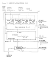
- FIG. 1 a prior art MIMD pipeline system is illustrated.
- a storage 10 stores a plurality of instruction streams, and in particular, the state of each such stream.
- An initialization control 12 is connected to the output of the storage 10, and a pipeline circuit 14 is connected to the output of the initialization control 12, the pipeline circuit 14 having no hazards detection circuit.
- the output of the pipeline 14 is connected to the storage 10.
- an instruction stream stored in storage 10 of Fig. 1, is transmitted to the initialization control 12.
- the initialization control 12 in response thereto, transmits each instruction of the instruction stream, one at a time, to the pipeline circuit 14.
- the instructions are piped within pipeline circuit 14 and executed, one at a time.
- updated instructions are transmitted from the pipeline circuit 14 for storage in storage 10.
- the last instruction of the instruction stream is transmitted to the pipeline circuit 14 from the initialization control 12, piped and executed therein, the last updated instruction of the original instruction stream is transmitted to storage 10.
- another instruction stream is transmitted from the storage 10 to the initialization control 12 for execution thereof in the pipeline circuit 14. It is evident that, in the configuration of Fig. 1, the original instruction stream must complete piping and execution within the pipeline circuit 14 before the next instruction stream may be transmitted from storage 10 to the initialization control 12 for piping and execution within the pipeline circuit 14. This is the limitation and disadvantage associated with the standard MIMD pipeline approach.
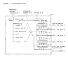
- a dynamic MIMD pipeline 20, according to the present invention is illustrated.
- the CBUS is connected to an instruction stack 20.1.
- An output of the instruction stack 20.1 is connected to a decode circuit 20.2.
- the decode circuit 20.2 output is connected to a handshakes and global hazards circuit 20.3, a mimd/sisd switch 20.4, and an initialization circuit 20.5.
- the outputs of the handshakes and global hazards circuit 20.3 and the mimd/sisd switch 20.4 are connected to the inputs of the initialization circuit 20.5.
- the initialization circuit 20.5 output is connected to a dynamic history table 20.7, to pipeline circuits 20.6, and to floating point registers (FPR) 20.8.
- FPR floating point registers
- the handshakes and global hazards circuit 20.3 output is also connected to an exception handler circuit 20.11, the output of which is further connected to the dynamic history table 20.7.
- Pipeline circuits 20.6 are also connected to the dynamic history table 20.7 and to the exception handler circuit 20.11, and produce an output which is conducted on a bus called the DBUS which is connected to the data cache, and conducted to the FPR 20.8 which is a local architecturally defined storage.
- the output of the dynamic history table 20.7 is used to control the gating of the output to the DBUS and to the FPR 20.8.
- the CBUS in addition to being input to the instruction stack 20.1, is also input to a DBUS stack controls 20.10 circuit.
- the output of the DBUS stack controls 20.10 circuit is connected to a DBUS stack 20.9, the input of which is connected to the DBUS.
- the output of the DBUS stack 20.9 and the output of the FPRs 20.8 generates the data which begins the data flow.
- the dynamic MIMD pipeline of the present invention may be subdivided into two paths: one for instructions and controls (CBUS path), and the other for data flow (DBUS path).
- CBUS path one for instructions and controls
- DBUS path the other for data flow
- the instructions are received via the CBUS and put in the instruction stack 20.1, and then decoded via decoder 20.2.
- the data is introduced into the dynamic MIMD pipeline of Fig. 2 via the DBUS.
- the handshakes and global hazards circuit 20.3 of Fig. 2 transmits "handshake" signals to the CPU and detects global hazards.
- a further construction of the handshakes and global hazards circuit 20.3 may be found in Fig. 10 of the drawings.
- a more detailed description of the handshakes and global hazards circuit 20.3 of Fig. 10 will be set forth below in one of the following paragraphs of this specification.
- the CBUS contains a set of handshake signals to be transmitted between the CPU to each PBU, including the FPU.
- the handshakes and global hazards circuit 20.3 of the FPU is required to send an acknowledge signal, a busy signal, or an interrupt signal back to the CPU if the CBUS request was sent from the CPU and the FPU is the only PBU involved in the request.
- the Acknowledge handshake signal is sent from the FPU to the CPU if a CBUS request is sent to the FPU and the FPU is not BUSY.
- the interrupt signal is sent from the FPU to the CPU if a data exception is encountered and critical information is stored in the status word.
- the busy handshake signal is sent from the FPU to the CPU if the FPU cannot accept another instruction for execution.
- the handshake signals, acknowledge, busy, interrupt, are sent to the CPU from the handshakes and global hazards circuit 20.3 of the FPU.
- Global hazards are detected in the handshakes and global hazards circuit 20.3 of the FPU and a signal is transmitted therefrom, for transmission to the initialization circuit 20.5, representative of the existence of such hazards.
- the handshake logic 20.3 (in connection with the initialization circuit 20.5) delivers the appropriate responses of the FPU to the other processor bus units (PBU). It also helps to detect the beginning and the end of an instruction stream.
- the global hazards circuit 20.3 detects the existence of hazards due to data dependencies of instructions on other executing instructions (data interlock).
- the MIMD/SISD switch 20.4 switches to either SISD mode or MIMD mode. If an incoming instruction involves operands more than 64 bits in length or if an instruction is determined to be difficult to execute, the MIMD/SISD switch 20.4 selects the SISD mode, otherwise it uses the MIMD mode.
- MIMD/SISD switch 20.4 to switch the pipeline mode to the MIMD mode:
- MIMD/SISD switch 20.4 will switch the pipeline mode to the SISD mode.
- the initialization circuit 20.5 of Fig. 2 starts the pipe, and updates the Dynamic History Table 20.7.
- a further construction of the initialization circuit 20.5 may be found in Fig. 11 of the drawings. A more detailed description of the initialization circuit 20.5 of Fig. 11 will be set forth below in one of the following paragraphs of this specification.
- the initialization circuit 20.5 determines the beginning and end of an instruction stream and determines if any data dependent hazards exist.
- the type of instruction is compared, in the initialization circuit 20.5 and the global hazard circuit 20.3, with the completion status of the first cycle status of the appropriate pipe to use, as indicated by the internal pipe controls 20.6a-d. If there is no global hazards, as indicated by the dynamic history table 20.7, and no immediate internal hazards exist, as indicated by the output of the handshakes and global hazards circuit 20.3, the instruction is initialized. If the BUSY handshake signal is developed by the handshakes and global hazards circuit 20.3, no initialization takes place in the initialization circuit 20.5. Initialization involves starting the status controls of the appropriate pipe and also entering a new line in the Dynamic History Table.
- the handshake controls 20.3 which sends the acknowledge signal to the CPU indicating that the instruction has been started or by sending a busy signal to the CPU, indicating that the FPU has the instruction but the pipe of incoming instructions had better be stopped because the FPU cannot handle very many more instructions.
- the initialization logic 20.5 and the global hazards logic 20.3 determine the beginning and end of a stream of instructions.
- the response "acknowledge” and “not busy” to an instruction not already in a stream indicates the beginning of a stream, and "busy” indicates the end of a stream.
- the global hazards circuit 20.3 is used to determine hazards due to data "dependencies".
- the initialization logic 20.5 adds new lines to the dynamic history table 20.7. Therefore, initialization consists of handshaking, updating the history file, and possibly dealing with data hazards.
- the dynamic MIMD pipeline of Fig. 2 includes four pipeline circuits 20.6: pipe1 20.6a, pipe2 20.6b, pipe3 20.6c, and pipe4 20.6d. Thus, there are four categories of instructions, one category for each pipe 20.6a through 20.6d.
- Data on the DBUS is processed by either the FPRs 20.8, or the DBUS stack 20.9 which is controlled by the DBUS stack controls 20.10.
- the exception handler 20.11 determines if there is an exception.
- the types of data exceptions that can occur while executing instructions are: Exponent Overflow Exception Exponent Underflow Exception Floating Point Divide Exception Fixed Point Divide Exception Significance Exception Square Root Exception
- the dynamic MIMD pipeline 20 disposed in the FPU of the computer system, receives instructions via the CBUS and the FPU responds back, as do the other processor bus units, by transmitting certain "handshake" signals including an ACKnowledge handshake signal, a BUSY handshake signal, and an INTerrupt handshake signal. Since the CPU works in a pipeline mode and sends PBO commands out every cycle, regardless of whether the last PBO was ACKnowledged, the PBUs must determine whether the last PBO was acknowledged before proceeding to execute the next PBO.
- the PBUs include a "smart" interface. Therefore, using the smart interface, a PBU must check on the handshakes of other PBUs with the CPU.
- a PBU is required to send one of the three handshake signals (from the handshakes circuit 20.3 of Fig. 2) to the CPU in the cycle after a PBO was received by the PBU. If hazards are encountered by a PBU, such as the FPU, a BUSY handshake signal is sent to the CPU by a PBU. When the BUSY signal is sent to the CPU, the PBU holds the received instruction and the following instruction in an instruction stack (such as instruction stack 20.1 of Fig. 2 for a FPU) so that the sequence of instructions received from the CPU can be maintained.
- an instruction stack such as instruction stack 20.1 of Fig. 2 for a FPU
- Instructions are not stacked unless hazards, which cause generation of the BUSY handshake signal, are encountered.
- the FPU accepts as many instructions as it can handle; however, the FPU does not contain as much information as is contained by the CPU, since the CPU can halt an instruction before the instruction is even sent to the bus units if it sees, in its buffer of instructions, that problems may be encountered.
- PBOs are sent from the CPU that require execution by the FPU and another bus unit, such as the data cache, the FPU has no power to prevent the data cache from starting the execution of the instruction.
- the most efficient method for the FPU to pipe is to go as far as possible until a hazard is encountered.
- Figs. 3a-3c a construction of the instruction stack 20.1 of Fig. 2 is illustrated.
- Fig. 3a illustrates the construction of the instruction stack 20.1
- Fig. 3b illustrates the bits on the CBUS during a hardwired mode
- Fig. 3c illustrates the bits on the CBUS during a microcode mode.
- the instruction stack 20.1 comprises the CBUS Stack register 20.1.1, and a CBUS register 20.1.2 connected to the output of the CBUS stack register 20.1.1.
- the instruction stack 20.1 as well as the CBUS consist of 25 bits of information for, at most, 2 instructions. This 25 bits of information comprise: bit 0 - the PBO bit which indicates whether the FPU is in a hardwired mode or a microcode mode; if in hardwired mode (0), exceptions are reported to the CPU; if in microcode mode (1), exceptions are stored in the status word (see Fig.
- bit 1 the FPU request bit which signals the FPU that this instruction must be executed by the FPU; bit 2 - the IPU/Cache request bit which signals the cache to decode the instruction; bit 3 - the VP request bit; bits 17 to 19 - in microcode mode, these bits are the SRC, source, identifier bits; bits 20 to 22 - in microcode mode, these bits are the DST, destination, identifier bits; bits 4 to 10 - the instruction opcode bits; bits 17 to 19 - in hardwired mode, these bits are the interrupt tag field which is stored in the status word on an exception; and bit 24 - the parity bit used for checking the validity of the instruction.
- the instruction on the CBUS is introduced into the instruction stack 20.1 via the CBUS bits defined above.
- the dynamic history table 20.7 comprises 17 bits of information stored away for at most 8 instructions at a time.
- the Dynamic History Table 20.7 consists of data that is needed when it is necessary for an incoming instruction to enter one of pipes 20.6a-20.6d and to complete from these pipes. Since the instructions are stacked, the table 20.7 provides a means of sequencing the completion of execution of instructions of one or more instruction streams.
- the limitation of the CBUS, to send one instruction at a time determines the instruction's starting time. Since the execution of the instructions of the one or more instruction streams may take multiple cycles to complete, and since there exists more than one pipe, it is possible that multiple instructions will be executing at the same time.
- the dynamic history table 20.7 stores the following information:
- the pipe number (PIPE NO) is critical because it sequences the multiple pipes of pipeline circuits 6a-6d of Fig. 2 (four in all). Sequencing is of very little concern in a one pipe system, but, with multiple pipes, tracking information must be maintained.
- the write address (WR ADDR), write type (WT), and result length (LEN) help in completing the instruction.
- the tag information (INT TAG) is stored away if an exception occurs and helps in identifying the exact instruction which caused the exception. If it is a SISD instruction, completion is sensed in a different way than looking to see if valid data is disposed at the end of a pipe, but instead, is determined by a counter which counts the cycles.
- the most important bit is the valid bit (V) which indicates whether the instruction in this entry of the stack is valid.
- the valid bit (V) is cleared when an exception occurs.
- the valid bit (V) entry is cleared and the stack is shifted upon completion of an instruction.
- a quick method is available to cancel all pending instructions in the FPU, that is, by clearing the valid bit (V) in the dynamic history table 20.7.
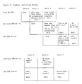
- Fig. 5 illustrates the construction of pipe1 20.6a which is used for add type instructions, such as add, subtract, divide, compares, and square roots.
- the Fig. 5 pipe functions in three cycles.
- Fig. 6 illustrates the construction of pipe2 20.6b, the multiply pipe, which functions in 5 cycles, and is used for multiply instructions.
- Fig. 7 illustrates the construction of pipe3 20.6c, which is used for load RX type instructions and functions in two cycles.
- Fig. 8 illustrates the construction of pipe4 20.6d, which is used for all other miscellaneous functions, and which are usually either a write or a read of some auxiliary or status registers.
- pipeline 20.6a includes a controls section and a pipe1 section.
- pipes 20.6b through 20.6d each include a controls section.
- the pipeline controls section of pipe 20.6a-20.6d controls the internal parts of each pipe by pushing the operations as far as possible through the pipes and sensing when the FPRs 20.8 are interlocked and by determining where good data can be found.
- pipeline 20.6 comprises four pipes: 20.6a through 20.6d. In MIMD mode, these pipes have different lengths thus creating complexities in controlling these pipes globally.
- the status fields for the registers in the add pipe of Fig. 5 consist of the operands FPR address (ADDR), whether SISD or MIMD mode is invoked (M/S), some bypass information (2BY), whether this stage in the pipe is for a valid instruction (VI), whether the data in the register is valid (VD), and whether the instruction is RX or RR type (RX).
- the status fields associated with the registers of the multiply pipe of Fig. 6 store this information and further information including the length of the operands (LI), whether it's a floating point or fixed point operand (FLP), and whether the data is still valid (VR), even if this stage of the pipe does not have a valid instruction.
- the other pipes do not need status information because they are very short.
- the status information for each stage of the pipe flags to the following stage its validity and then, in the following cycle, the next stage becomes valid if there are no contentions.
- the flags help in determining contention and push the instruction's data as far as it can through the pipe.
- pipe1 (add) internal control registers 20.6a are illustrated.
- pipe1 20.6a includes an alignment register 20.6a.4, an FA register 20.6a.1, an FB register 20.6a.2, an A register 20.6a.5, a B register 20.6a.6, an adder 20.6a.7, an FS register 20.6a.3, an S register 20.6a.8, and a post normalizer register 20.6a.9.
- status fields associated with the FA register 20.6a.1, FB register 20.6a.2, and FS register 20.6a.3 are illustrated.
- Fig. 5 illustrates the add pipe 20.6a and its associated internal pipe control registers.
- the add pipe of Fig. 5 consists of three cycles. During the first cycle, the data is retrieved from either the FPRs 20.8 and/or from the DBUS. Alignment is accomplished by the alignment hardware 20.6a.4. Operands are latched into A register 20.6a.5 and B register 20.6a.6. In cycle two, the actual add is performed by the adder 20.6a.7 and the result is stored in S register 20.6a.8. In the third and final cycle, the post normalizer 20.6a.9 shifts out leading zeros if required and the data is sent back to the FPRs 20.8. The previously described function reflects the manner in which the pipe handles add instructions.
- FIG. 5b the status fields for the FA register 20.6a.1, FB register 20.6a.2, and FS register 20.6a.3 are illustrated.
- Such status fields include the following bits:
- pipe2 20.6b the multiply pipe, includes FXA register 20.6b.1, FYS register 20.6b.2, FXB register 20.6b.3, FY register 20.6b.4, FP register 20.6b.5, XA register 20.6b.6, 3X hardware 20.6b.7, XB and 3X registers 20.6b.8, Y register 20.6b.9, M1 hardware 20.6b.10, M2 hardware 20.6b.11, and P register 20.6b.12.
- the multiply pipe consists of 5 cycles if no hazards are encountered:
- the control registers that control this pipe are: the FXA register 20.6b.1, which maintains the status of XA register 20.6b.6; the FYS register 20.6b.2, which maintains the status of a temporary register that initially gets operand 2 on an RR instruction; the FXB register 20.6b.3; the FY register 20.6b.4; and the FP register 20.6b.5, which maintain the status of their associated paired data registers.
- These status registers maintain 12 bits of information, as described by Fig. 6b.
- a description of each field of the control registers (the FXA register 20.6b.1, the FYS register 20.6b.2, the FXB register 20.6b.3, the FY register 20.6b.4, and the FP register 20.6b.5), is illustrated.
- the FXA register 20.6b.1 and FYS register 20.6b.2 are set in cycle one by the initialization hardware 20.5. If there is no "contention" on the XB, 3X registers 20.6b.8, the FXB register 20.6b.3 is set from FXA register 20.6b.1. If there is no "contention” on Y register 20.6b.9, the FY register 20.6b.4 is set by the initialization hardware 20.5 or FYS register 20.6b.2.
- "Contention" can take the form of: M1 valid, or M2 valid and P register contention, or XA already valid for previous multiply and XB contention
- the FP register 20.6b.5 is set by FXB register 20.6b.3 when M2 is valid and there is no contention on P register 20.6b.12.
- the valid result bit of the FP register 20.6b.5 is maintained separately since it is dependent on other writes to the FPRs.
- the multiply pipe is maintained by the internal pipe controls which push the data as far as possible through the pipe until internal hazards are encountered or until the P register 20.6b.12 is valid and no external hazards are encountered which prevent the instructions in this pipe from completing.
- pipe3 20.6c which is used for load RX type instructions, is illustrated.
- the pipe3 20.6c consists of two cycles, during which there is no execution of data, rather, data merely flows through the pipe.
- the instruction is decoded via decoder 20.2 and the FPU waits for the appropriate DBUS valid signal from the DBUS stack controls 20.10.
- the data being received and gated into DREG 20.9.1 of the DBUS stack 20.9, is received during cycle 1. Then, the data is sent to the FPRs 20.8 during cycle 2.
- the controls which monitor this are the DREG Valid register 20.10.1 of the DBUS stack controls 20.10 and the rest of the DBUS stack controls 20.10.
- pipe4 20.6d which performs miscellaneous functions, is illustrated.
- pipe4 20.6d comprises indirect address registers (IND ADDR REGs) 20.6d.1 connected to an output of the DREG 20.9.1 which forms a part of the DBUS stack 20.9 of Fig. 2, status word register 20.6d.2 connected to the output of the DREG 20.9.1, retry status register 20.6d.3 connected to a CBUS register, and an indirect address mode register 20.6d.4 connected to the CBUS register.
- the status word register 20.6d.2 and the retry status register 20.6d.3 are connected, at their outputs, to the DREG 20.9.1 and to the FPRs 20.8.
- the indirect address registers 20.6d.1 are used in microcode mode and contain FPR 20.8 addresses.
- the status word registers 20.6d.2 maintain the status of the FPU, such status consisting of exception status information and the status of the checkers.
- DBUS stack 20.9 and DBUS stack controls 20.10 are illustrated.
- the DBUS stack controls 20.10 comprise the DREG valid register 20.10.1, the DCBUS Register 20.10.2, the decoder 20.10.3, the DS5 register 20.10.4, the DS4 register 20.10.5, the DS3 register 20.10.6, the DS2 register 20.10.7, the DS1 register 20.10.8, the S2 valid register 20.10.9, the S1 valid register 20.10.10, and the mux select logic 20.10.11.
- the DBUS stack 20.9 comprises the S2 register 20.9.3 connected to the DBUS, the S1 register 20.9.2 connected to the output of the S2 register and to the DBUS, and the DREG register 20.9.1 connected to the output of the S1 register and the DBUS.
- bits within registers DS1- DS5 (20.10.8 through 20.10.4, respectively, of Fig. 9a) include the following:
- Data for an operation involving normal RR operations, comes from the FPRs 20.8, unless an interlock exists, in which case, the local pipe controls find the appropriate data by comparing address fields of status registers of all the pipes. For RX operations, it is a little more difficult; operand one is found in the same way, but operand two comes from the data bus. Since the data cache or another bus unit is requested to supply the data at the same time that the FPU receives the instruction, and the other bus unit, which is requested to supply the data, may be BUSY, the receipt of the data by the FPU may be out of synchronization with the receipt of the instruction by the FPU. As a result, underflow or overflow of the data may exist.
- the DBUS stack controls 20.10 inform the local pipe controls 20.6 when the DREG 20.9.1 is valid for their appropriate pipe. This is vital in separating the data, especially when several pipes are starved of data from the data bus and the data bus becomes valid. Therefore, the DBUS stack controls 20.10 sequences the data with the instructions. After this is accomplished, the pipe controls 20.6 move the data through the pipe and await the approval of the global Dynamic History Table 20.7 to approve the completion of the instruction (as will be discussed later, completion consists of comparing the pipe number of the oldest instruction in the dynamic history table 20.7 file, i.e., the lowermost entry in the table, with the pipe number of the pipe in question). Thus, the Data Flow is controlled from start to finish.
- the data bus stack controls 20.10 are needed since the memory supplies the data when it can, independently of when the data is requested.
- Underflow occurs when the memory is slow in supplying the data and several pipes have been initialized, except for the absence of an operand from memory (RX type). Since several pipes may be waiting for data, when it finally arrives, controls are needed for sorting out to which pipe the incoming data should be transmitted.
- Overflow occurs when a pipe or several pipes are full and several instructions, which use the data from memory, are transmitted from the CPU to the floating point unit (FPU) and memory simultaneously; this causes the memory to send the data to the floating point unit, since it cannot immediately put the data into an appropriate pipe. Therefore, the data must be stacked and identified with the appropriate pipe number to which the data must eventually be transmitted.
- handshakes and global hazards circuit 20.3 comprises a pipe1 new instruction contentions circuit 20.3.1, a pipe2 new instruction contention circuit 20.3.2, a pipe3 new instruction contention circuit 20.3.3, and a pipe4 new instruction contention circuit 20.3.4, all of which are connected to the internal pipe controls 20.6, and to the decode circuit 20.2 of Fig.
- a global contention circuit 20.3.5 connected to the dynamic history table 20.7 and responsive to other unit handshakes for transmitting a "FPU BUSY” signal to the computer system CPU and for transmitting a "UNIT BUSY” signal to the initialization circuit 20.5;
- a handshakes combinatorial logic circuit 20.3.6 is connected to the global contention circuit 20.3.5 and is responsive to the other unit handshakes for transmitting a "FPU ACK” (floating point unit acknowledge) signal to the computer system CPU and for transmitting a "VALID INSTR” (valid instruction) signal to the initialization circuit 20.5; and an interrupt handshakes combinatorial logic circuit 20.3.7 connected to the handshakes combinatorial logic 20.3.6 and to the exception handler circuit 20.11 for transmitting a "FPU INTERRUPT" (floating point unit interrupt) signal to the computer system CPU.
- the inputs to the handshakes and global hazard circuit 20.3 include the handshakes from the other PBUs, the internal pipe controls 20.6, the dynamic history table 20.7, and the decode circuit 20.2.
- the "decode circuit” input informs the handshakes circuit 20.3 if there is a new instruction on the CBUS and in which pipe the new instruction needs to be executed.
- the "internal pipe controls” input indicates, for each pipe, whether there are any hazards in the first stage of the pipe.
- the "other unit handshakes” input is monitored by the handshakes circuit 20.3 to see if hazards exist external to the FPU.
- the "dynamic history table” input indicates if there are any internal global hazards.
- FPU ACK (acknowledge) is sent from the handshake combinational logic to the CPU and the other bus units (except in the case where the instruction is for more than one bus unit and then the acknowledge is suppressed). If there exists a new instruction but there exists hazards or contentions, then "UNIT BUSY” is sent to the initialization circuit and "FPU BUSY” is sent to the CPU and the other PBUs; in addition, the new instruction is held in CBUS register 20.1.2 of the instruction stack 20.1 of Fig. 3 and is again considered as a new instruction in the next cycle and subsequently until there exists a cycle during which it can be acknowledged.
- VALID INSTR (valid instruction) is sent to the initialization circuit and is an early signal which indicates that the instruction in the CBUS register has the proper CPU handshakes to indicate that it is an instruction that the FPU should execute; this is independent of hazards and contentions.
- the last signal which is sent from this unit is "FPU INTERRUPT” which is sent to the CPU indicating an exception condition.
- This signal must be gated from the exception handler 20.11 which determines the exception condition, because it is dependent on the response of the other PBUs to previous instructions. In a pipelined computer, several instructions are issued and executed in parallel. As a result, several exceptions can occur in the same cycle. Since the instruction set is SISD, exceptions must be handled as though the instructions were executed sequentially. This is done by gating the FPU INTERRUPT signal with conditions determined from the handshake controls. Thus, handshake and global hazard detection is accomplished by the handshakes and global hazards circuit 20.3 in Fig. 10 and Fig. 2.
- the initialization circuit 20.5 is illustrated.
- the initialization circuit 20.5 is responsive to an output signal from the handshakes and global hazards circuit 20.3, the decode circuit 20.2, and the mimd/sisd switch 20.4.
- the output signal from the handshakes and global hazards circuit 20.3 includes the VALID INSTRUCTION signal and the ACKNOWLEDGE signal.
- the output signal from the decode circuit 20.2 includes the following information: length information (LENGTH) relating to the length of the instruction's data (short length data must be zero-filled); write type (WRITE TYPE) information providing address information when a write to the floating point registers (FPRs) 20.8 is being performed; fpr address information (FPR ADDRESSES) relating to address information when data is being retrieved from the FPRs 20.8; RX instruction information (RX) indicating whether the instruction being input to the initialization circuit 20.5 is an RX type instruction (for an RX type instruction, the second portion of the instruction's data comes from the main memory via the DBUS, not from the FPRs 20.8); "etc", which may provide any other information needed by the pipe controls for pipes 20.6a-20.6d; and the pipe number (PIPE NO) which provides the pipe number, the identifier of one of pipes 20.6a-20.6d.
- LENGTH length information
- WRITE TYPE write type
- FPR ADDRESSES
- the decode circuit 20.2 provides the pipe number because each of the pipes 20.6a-20.6d are specialized to function in association with special instructions and the decode circuit 20.2 knows, by virtue of its decode function, what type of instruction is being input to the initialization circuit 20.5 and therefore what pipe into which the incoming special instruction should be inserted for execution.
- the output of the mimd/sisd switch 20.4 provides information relating to the "position" of mimd/sisd switch 20.4.
- the initialization circuit 20.5 comprises a first multiplexer 20.5.1, a second multiplexer 20.5.2, a third multiplexer 20.5.3, a fourth multiplexer 20.5.4 and a fifth multiplexer 20.5.5, each multiplexer receiving the same selection signal and the same information signal.
- the selection signal selects the specific multiplexer, depending upon the binary bit representation of the selection signal.
- the information signal passes through the selected multiplexer, selected in accordance with the selection signal.
- the selection signal comprises the (1) VALID INSTRUCTION/ACKNOWLEDGE signal output from the handshakes and global hazards logic 20.3, and the (2) pipe number "pipe no" output from the decode logic 20.2.
- the information signal comprises (1) length, (2) write type, (3) FPR addresses, (4) RX, (5) MIMD/SISD, and (6) other information (etc).
- the information signal including the length information, the write type information, the FPR address information, the RX instruction information, the MIMD/SISD switch information, and the other information, is passed to one of pipes 20.6a-20.6d and/or to the dynamic history table 20.7.
- a plurality of instruction streams each containing a plurality of instructions, await execution by processors disposed within the pipeline circuits 6 of Fig. 2.
- a selection circuit selects from among the plurality of instruction streams, instructions which shall be input to the dynamic MIMD pipeline 20 of Fig. 2. These instructions are input, one by one, to the dynamic MIMD pipeline 20 via the CBUS.
- an instruction is transmitted to the dynamic MIMD pipeline 20 disposed in the FPU of Fig. 2, via the CBUS, it is decoded via decoder 20.2 and a determination is made whether such instruction is one which may be executed by the FPU.
- the FPU will: decode the instructions, one at a time, via decoder 20.2, decide if the pipeline will operate in SISD or MIMD mode, via switch 20.4, determine if any hazards exist, via global hazards logic 20.3, determine, via the decode logic 20.2 and the initialization logic 20.5, which pipe, 20.6a-20.6d, will execute the instruction, decide via the dynamic history table 20.7 when the appropriate pipe 20.6a-20.6d will complete so that the incoming instruction may be inserted therein for execution, and, when all the above is accomplished, the FPU will attempt to execute the instruction(s) by entering the pipeline structure 20.6 at a maximum rate, one at a time.
- the initialization logic 20.5 along with the global hazard circuit 20.3 will decide if a stream is beginning or ending and will appropriately inform the CPU of normal or abnormal endings of a stream of instructions as well as single instructions. Due to the potential existence of hazards, the initialization logic 20.5, together with the global hazard control logic 20.3, will decide when one of pipelines, 20.6a-20.6d, shall be utilized and when instructions are needed. Recall that the pipes 20.6a-20.6d are each specialized to handle certain categories of instructions. When an incoming new instruction is decoded via decoder 20.2, the type of instruction is determined and thus the particular pipe to use is identified.
- the initialization logic 20.5 receives the pipe number from the decode logic 20.2, and, via multiplexers 20.5.1-20.5.5, transmits the new instruction to its corresponding pipeline circuit, one of 20.6a-20.6d, in accordance with the received pipe number.
- the dynamic history table 20.7 is updated to record the identity of the pipe in which the instruction is disposed for execution. Since the pipes 20.6a-20.6d are connected to the dynamic history table 20.7 in feedback fashion, the status of execution of the particular instruction in the pipe is continuously recorded in the dynamic history table 20.7.
- the pipe X is full of instructions and the oldest instruction in the pipe X must complete before the further new instruction can enter for execution.
- the oldest (lowermost) entry in the table 20.7 indicates pipe number X in the pipe number column, the oldest instruction in pipe X is allowed to complete, making room for insertion of the further new instruction for execution.
- the table 20.7 with the internal pipe controls for pipes 20.6a-d are continuously consulted to assure that the proper utilization of all single pipelines is achieved, and instructions are executed from beginning to end in a proper manner.
- Each pipeline, one of 20.6a-20.6d, will execute a category of instructions and will be controlled externally by the information stored in the dynamic history table 20.7 and the initialization logic 20.5 and internally by the internal pipe controls.
- each pipeline, one of 20.6a-20.6d will be executing more than one instruction pertaining to a multiple number of instruction streams and each pipeline, one of 20.6a-20.6d, is controlled by its corresponding internal pipeline controls (see 20.6a-20.6d) to guarantee maximum utilization of the pipeline.
- the incoming instruction is put into a line of the dynamic history table 20.7.
- This table 20.7 contains a few parameters which are necessary in order to determine how to complete the incoming instruction.
- the key parameter is the pipe number (PIPE NO) which indicates in which pipe an instruction in one of the pipes is disposed.
- PIPE NO the pipe number
- the history table 20.7 is read each cycle to indicate which pipe, 20.6a-20.6d of pipeline circuit 20.6, will be the next pipe to complete the execution of an incoming instruction.
- the information read from table 20.7 is then compared with the internal status of the selected pipe (via its status registers) to see if the pipe is waiting to complete. If so, the instruction is completed and the corresponding entry in the dynamic history table 20.7 is erased from the history table 20.7 file.
- completion of the oldest one of such instructions in pipe X consists of comparing the parameters stored in table 20.7 associated with oldest (lowermost) instruction in the dynamic history table 20.7 file with the status of the pipe X, as indicated by its status registers.
- Fig. 9a there are two stacks: one stack for instructions, i.e., DS1 to DS5 registers 20.10.8 to 20.10.4 of the DBUS stack controls 20.10, and one stack for data, i.e., the DREG 20.9.1, the S1 register 20.9.2, and the S2 register 20.9.3 of the DBUS stack 20.9.
- the stack of instructions are obtained by decoding the CBUS; to do this, another register is needed, the DCBUS register 20.10.2, which latches the CBUS every cycle independent of the busy signals.
- the Decode hardware 20.10.3, combined with knowledge of the previous busys, indicates when a new DBUS load instruction enters the FPU.
- DREG valid 20.10.1, S1 valid 20.10.10, and S2 valid 20.10.9 are important status registers, each of which comprise two bits, each indicating whether the data is partially or fully valid.
- Overflow of data occurs when instructions are in the DS registers 20.10.4-20.10.8 but are not executing and data is in the data stack 20.9.1-20.9.3.
- Underflow of data occurs when several instructions are in the DS registers 20.10.4-20.10.8 but not enough data is in the data stack 20.9.1-20.9.3.
- Incoming data is stacked in the S2, S1, and DREG registers 20.9.3 through 20.9.1, respectively, of the DBUS stack 20.9, and incoming instructions are stacked in the DS5 through DS1 registers 20.10.4 through 20.10.8 of the DBUS stack controls 20.10, there being a one-to-one correspondence between the stacked instructions needing DBUS data and the stacked data. Since the incoming data is stacked in the DBUS stack 20.9, and the incoming instructions are stacked in the DBUS stack controls 20.10, when a set of data arrives on the DBUS and is ready for placement in one of pipes 20.6a-20.6d, it is necessary to determine which pipe, one of 20.6a-20.6d, gets the set of data.
- the arriving set of data goes to the pipe (one of 20.6a-20.6d) whose number is stored in bit positions 3 and 4 of the lowest one of the data stack control registers DS5-DS1, the DS1 register 20.10.8 (recall that bits 3 and 4 within the registers DS1-DS5 are the pipe number, to uniquely identify the pipe to which the data should be transmitted).
- FIG. 12 in order to further describe the functional operation of the dynamic MIMD pipeline of the present invention, a simple instruction stream is illustrated. With the assistance of Figs. 2 through 11, the manner by which the instruction stream flows through hardware of Fig. 2 is set forth in the following paragraphs.
- Cycle 0 - The CPU sends a load RX instruction to the FPU on the CBUS and the CBUS is latched into CBUS register 20.1.2 of Fig. 3 and DCBUS register 20.10.2 of Fig. 9.
- the load RX is decoded by the decode circuit 20.2 in Fig. 2 and decode circuit 20.10.3 of the DBUS stack controls 20.10 in Fig. 9.
- the handshakes and global hazard circuit 20.3 of Fig. 2 and Fig. 10 determines, by checking internal pipe control of pipe 3 20.6c, that there are no problems for a load instruction to begin and no global hazards exist, as determined by checking the dynamic history table 20.7.
- an acknowledge signal (FPU ACK) is sent from the handshakes and global hazards circuit 20.3 to the initialization circuit 20.5 which initializes pipe3 20.6c (FPU ACK is not sent to the other bus units because the data cache responds for both units in the case of a multi-bus unit PBO).
- the initialization hardware 20.5 also provides information to place the load instruction in the dynamic history table 20.7.
- the DBUS stack controls 20.10 place information about the load instruction into DS1 register 20.10.8 of Fig. 9 since the decode 20.10.3 of Fig. 9 determined it was an RX instruction. Also, a data valid signal was received on the DBUS, the signal being latched into DREG 20.9.1 of the DBUS stack 20.9; as a result, DREG valid latch 20.10.1 of the DBUS stack controls 20.10 becomes active.
- the CPU sends a multiply RR instruction to the FPU on the CBUS and this instruction on the CBUS is latched into CBUS register 20.1.2 of the instruction stack 20.1 and into the DCBUS register 20.10.2 of the DBUS stack controls 20.10.
- Cycle 2 - The multiply RR instruction is decoded by the decode circuit 20.2 in Fig. 2 and decode circuit 20.10.3 in Fig. 9.
- the handshakes and global hazard circuit 20.3 of Fig. 2 and Fig. 10 determines, from checking internal pipe control of pipe2 20.6b, that there are no problems for a multiply to begin and no global hazards exist, as determined from checking the dynamic history table 20.7.
- an acknowledge signal (FPU ACK) is sent to the CPU and to the other PBUs; the initialization circuit 20.5 initializes pipe2 20.6b and also reads FPR2 out of the FPRs 20.8 onto the FLPBUS of Fig. 6 to be latched into Y register 20.6b.9.
- the initialization hardware 20.5 also provides information to place the multiply instruction in the dynamic history table 20.7.
- the initialization hardware 20.5 also notices, from the global hazard logic 20.3 which decoded the dynamic history table 20.7, that FPR 1 is interlocked by the load instruction and thus operand 1 of the multiply is interlocked.
- the initialization hardware 20.5 from information from the decode 20.2, initializes the control registers FXA 20.6b.1 and FY register 20.6b.6.
- the DBUS stack controls decode circuit 20.10.3 of Fig. 9 determined that the multiply RR instruction does not use the DBUS but, rather, is interlocked by DREG 20.9.1 and thus DREG 20.9.1 is loaded into XA register 20.6b.6 of Fig. 6.
- the DREG 20.9.1 is valid this cycle and the FPRs 20.8 are loaded (written into) to complete the load instruction (the completion of the load instruction is allowed to occur as a result of the DREG valid register 20.10.1 of Fig. 9 and the dynamic history table 20.7 which indicated that the next pipe to complete is pipe 3).
- the CPU sends an add RR instruction to the FPU on the CBUS and the CBUS is latched into CBUS register 20.1.2 of the instruction stack 20.1 and DCBUS register 20.10.2 of the DBUS stack controls 20.10.
- Cycle 3 The add RR instruction is decoded by the decode circuit 20.2 in Fig. 2 and decode circuit 20.10.3 in Fig. 9.
- the handshakes and global hazard circuit 20.3 of Fig. 2 and Fig. 10 determines, from checking internal pipe control of pipe1 20.6a, that there are no problems for an add to begin and no global hazards exist, as determined from checking the dynamic history table 20.7. Thus an acknowledge signal (FPU ACK) is sent from the handshakes circuit 20.3 to the CPU and the other PBUs.
- the initialization circuit 20.5 initializes pipe1 20.6a and also reads FPR3 and FPR4 out of the FPRs 20.8 into A register 20.6a.5 and B register 20.6a.6 of Fig. 5.
- the initialization hardware 20.5 also provides information to place the add instruction in the dynamic history table 20.7 and notices, from the global hazard logic 20.3 which decoded the dynamic history table 20.7, that no interlock exists. From information provided from the decode circuits, the initialization hardware 20.5 initializes the control registers, FA register 20.6a.1 and FB register 20.6a.2 of Fig. 5. In Fig. 6, the multiply hardware holds the value in Y register 20.6b.9, due to contentions determined by the mux select logic 20.6b.13, performs a 3X calculation, via 3X hardware 20.6b.7, and latches XB and 3X registers 20.6b.8. The control information for the multiply instruction is held in FY register 20.6b.4 of Fig. 6 and is transferred from FXA register 20.6b.1 to FXB register 20.6b.3. In Fig. 5, the align 20.6a.4 of the add instruction is also accomplished during this cycle.
Landscapes
- Engineering & Computer Science (AREA)
- Theoretical Computer Science (AREA)
- Software Systems (AREA)
- Physics & Mathematics (AREA)
- General Engineering & Computer Science (AREA)
- General Physics & Mathematics (AREA)
- Computer Hardware Design (AREA)
- Computing Systems (AREA)
- Multimedia (AREA)
- Advance Control (AREA)
- Multi Processors (AREA)
Applications Claiming Priority (2)
| Application Number | Priority Date | Filing Date | Title |
|---|---|---|---|
| US102985 | 1987-09-30 | ||
| US07/102,985 US4916652A (en) | 1987-09-30 | 1987-09-30 | Dynamic multiple instruction stream multiple data multiple pipeline apparatus for floating-point single instruction stream single data architectures |
Publications (3)
| Publication Number | Publication Date |
|---|---|
| EP0328721A2 true EP0328721A2 (de) | 1989-08-23 |
| EP0328721A3 EP0328721A3 (en) | 1990-07-18 |
| EP0328721B1 EP0328721B1 (de) | 1995-04-05 |
Family
ID=22292751
Family Applications (1)
| Application Number | Title | Priority Date | Filing Date |
|---|---|---|---|
| EP88109842A Expired - Lifetime EP0328721B1 (de) | 1987-09-30 | 1988-06-21 | Dynamische Mehrbefehle-Mehrdaten-Mehrpipeline-Gleitpunkteinheit |
Country Status (6)
| Country | Link |
|---|---|
| US (1) | US4916652A (de) |
| EP (1) | EP0328721B1 (de) |
| JP (1) | JPH01102644A (de) |
| BR (1) | BR8804969A (de) |
| CA (1) | CA1313273C (de) |
| DE (1) | DE3853529T2 (de) |
Cited By (11)
| Publication number | Priority date | Publication date | Assignee | Title |
|---|---|---|---|---|
| EP0381471A2 (de) * | 1989-02-03 | 1990-08-08 | Digital Equipment Corporation | Verfahren und Vorrichtung zur Vorverarbeitung mehrerer Befehle in einem Pipeline-Prozessor |
| EP0490524A2 (de) * | 1990-12-07 | 1992-06-17 | International Business Machines Corporation | Pipeline-Verfahren und -Gerät |
| EP0507251A1 (de) * | 1991-04-01 | 1992-10-07 | Matsushita Electric Industrial Co., Ltd. | Befehlspipelinesynchronisierungsverfahren und Pipelinerechner unter Verwendung dieses Verfahrens |
| EP0619557A2 (de) * | 1993-03-31 | 1994-10-12 | Motorola, Inc. | Datenverarbeitungssystem- und methode |
| WO1999042923A1 (de) * | 1998-02-19 | 1999-08-26 | Infineon Technologies Ag | Vorrichtung zur hierarchischen und verteilten steuerung von programmierbaren modulen in hochintegrierten systemen |
| GB2348973A (en) * | 1999-04-09 | 2000-10-18 | Pixelfusion Ltd | SIMD array with array controller |
| US6311262B1 (en) | 1999-01-18 | 2001-10-30 | Infineon Technologies Ag | Apparatus for the hierarchical and distributed control of programmable modules in large-scale integrated systems |
| US7506136B2 (en) | 1999-04-09 | 2009-03-17 | Clearspeed Technology Plc | Parallel data processing apparatus |
| US7526630B2 (en) | 1999-04-09 | 2009-04-28 | Clearspeed Technology, Plc | Parallel data processing apparatus |
| US7627736B2 (en) | 1999-04-09 | 2009-12-01 | Clearspeed Technology Plc | Thread manager to control an array of processing elements |
| US7802079B2 (en) | 1999-04-09 | 2010-09-21 | Clearspeed Technology Limited | Parallel data processing apparatus |
Families Citing this family (153)
| Publication number | Priority date | Publication date | Assignee | Title |
|---|---|---|---|---|
| US5241635A (en) * | 1988-11-18 | 1993-08-31 | Massachusetts Institute Of Technology | Tagged token data processing system with operand matching in activation frames |
| US5333287A (en) * | 1988-12-21 | 1994-07-26 | International Business Machines Corporation | System for executing microinstruction routines by using hardware to calculate initialization parameters required therefore based upon processor status and control parameters |
| US5768575A (en) * | 1989-02-24 | 1998-06-16 | Advanced Micro Devices, Inc. | Semi-Autonomous RISC pipelines for overlapped execution of RISC-like instructions within the multiple superscalar execution units of a processor having distributed pipeline control for sepculative and out-of-order execution of complex instructions |
| JP3153906B2 (ja) * | 1989-02-24 | 2001-04-09 | アドヴァンスド マイクロ デヴァイセス インコーポレイテッド | コンピュータの分散型パイプライン制御装置及び方法 |
| US5226126A (en) * | 1989-02-24 | 1993-07-06 | Nexgen Microsystems | Processor having plurality of functional units for orderly retiring outstanding operations based upon its associated tags |
| US5781753A (en) | 1989-02-24 | 1998-07-14 | Advanced Micro Devices, Inc. | Semi-autonomous RISC pipelines for overlapped execution of RISC-like instructions within the multiple superscalar execution units of a processor having distributed pipeline control for speculative and out-of-order execution of complex instructions |
| JPH0719222B2 (ja) * | 1989-03-30 | 1995-03-06 | 日本電気株式会社 | ストアバッフア |
| JPH0640316B2 (ja) * | 1989-04-20 | 1994-05-25 | 工業技術院長 | 演算レジスタ上でのデータ待ち合せ実現方法 |
| CA2016068C (en) * | 1989-05-24 | 2000-04-04 | Robert W. Horst | Multiple instruction issue computer architecture |
| US5317734A (en) * | 1989-08-29 | 1994-05-31 | North American Philips Corporation | Method of synchronizing parallel processors employing channels and compiling method minimizing cross-processor data dependencies |
| EP0827070B1 (de) * | 1989-09-25 | 1999-08-04 | Matsushita Electric Industrial Co., Ltd. | Rechner mit Pipeline-Struktur |
| US5185871A (en) * | 1989-12-26 | 1993-02-09 | International Business Machines Corporation | Coordination of out-of-sequence fetching between multiple processors using re-execution of instructions |
| JP2818249B2 (ja) * | 1990-03-30 | 1998-10-30 | 株式会社東芝 | 電子計算機 |
| JP2771683B2 (ja) * | 1990-07-17 | 1998-07-02 | 三菱電機株式会社 | 並列処理方式 |
| US5163139A (en) * | 1990-08-29 | 1992-11-10 | Hitachi America, Ltd. | Instruction preprocessor for conditionally combining short memory instructions into virtual long instructions |
| US5794059A (en) * | 1990-11-13 | 1998-08-11 | International Business Machines Corporation | N-dimensional modified hypercube |
| US5963745A (en) * | 1990-11-13 | 1999-10-05 | International Business Machines Corporation | APAP I/O programmable router |
| US5625836A (en) * | 1990-11-13 | 1997-04-29 | International Business Machines Corporation | SIMD/MIMD processing memory element (PME) |
| US5588152A (en) * | 1990-11-13 | 1996-12-24 | International Business Machines Corporation | Advanced parallel processor including advanced support hardware |
| US5809292A (en) * | 1990-11-13 | 1998-09-15 | International Business Machines Corporation | Floating point for simid array machine |
| US5765015A (en) * | 1990-11-13 | 1998-06-09 | International Business Machines Corporation | Slide network for an array processor |
| ATE180586T1 (de) * | 1990-11-13 | 1999-06-15 | Ibm | Paralleles assoziativprozessor-system |
| US5734921A (en) * | 1990-11-13 | 1998-03-31 | International Business Machines Corporation | Advanced parallel array processor computer package |
| US5765011A (en) * | 1990-11-13 | 1998-06-09 | International Business Machines Corporation | Parallel processing system having a synchronous SIMD processing with processing elements emulating SIMD operation using individual instruction streams |
| US5590345A (en) * | 1990-11-13 | 1996-12-31 | International Business Machines Corporation | Advanced parallel array processor(APAP) |
| US5828894A (en) * | 1990-11-13 | 1998-10-27 | International Business Machines Corporation | Array processor having grouping of SIMD pickets |
| US5765012A (en) * | 1990-11-13 | 1998-06-09 | International Business Machines Corporation | Controller for a SIMD/MIMD array having an instruction sequencer utilizing a canned routine library |
| US5966528A (en) * | 1990-11-13 | 1999-10-12 | International Business Machines Corporation | SIMD/MIMD array processor with vector processing |
| US5752067A (en) * | 1990-11-13 | 1998-05-12 | International Business Machines Corporation | Fully scalable parallel processing system having asynchronous SIMD processing |
| US5963746A (en) * | 1990-11-13 | 1999-10-05 | International Business Machines Corporation | Fully distributed processing memory element |
| US5630162A (en) * | 1990-11-13 | 1997-05-13 | International Business Machines Corporation | Array processor dotted communication network based on H-DOTs |
| US5815723A (en) * | 1990-11-13 | 1998-09-29 | International Business Machines Corporation | Picket autonomy on a SIMD machine |
| JP2925818B2 (ja) * | 1991-04-05 | 1999-07-28 | 株式会社東芝 | 並列処理制御装置 |
| JP2642529B2 (ja) * | 1991-04-30 | 1997-08-20 | 株式会社東芝 | 並列プロセッサーの命令分配処理装置 |
| US5594918A (en) * | 1991-05-13 | 1997-01-14 | International Business Machines Corporation | Parallel computer system providing multi-ported intelligent memory |
| JP2908598B2 (ja) * | 1991-06-06 | 1999-06-21 | 松下電器産業株式会社 | 情報処理装置 |
| JPH04367936A (ja) | 1991-06-17 | 1992-12-21 | Mitsubishi Electric Corp | スーパースカラープロセッサ |
| US5363495A (en) * | 1991-08-26 | 1994-11-08 | International Business Machines Corporation | Data processing system with multiple execution units capable of executing instructions out of sequence |
| US5283874A (en) * | 1991-10-21 | 1994-02-01 | Intel Corporation | Cross coupling mechanisms for simultaneously completing consecutive pipeline instructions even if they begin to process at the same microprocessor of the issue fee |
| CA2073516A1 (en) * | 1991-11-27 | 1993-05-28 | Peter Michael Kogge | Dynamic multi-mode parallel processor array architecture computer system |
| JP2642039B2 (ja) * | 1992-05-22 | 1997-08-20 | インターナショナル・ビジネス・マシーンズ・コーポレイション | アレイ・プロセッサ |
| DE69329778T2 (de) | 1992-09-29 | 2001-04-26 | Seiko Epson Corp | System und verfahren zur handhabung von laden und/oder speichern in einem superskalar mikroprozessor |
| US6735685B1 (en) * | 1992-09-29 | 2004-05-11 | Seiko Epson Corporation | System and method for handling load and/or store operations in a superscalar microprocessor |
| JP3338488B2 (ja) * | 1992-11-18 | 2002-10-28 | 富士通株式会社 | データ処理装置の検証方法及び装置 |
| US5761473A (en) * | 1993-01-08 | 1998-06-02 | International Business Machines Corporation | Method and system for increased instruction synchronization efficiency in a superscalar processsor system utilizing partial data dependency interlocking |
| JPH06242948A (ja) * | 1993-02-16 | 1994-09-02 | Fujitsu Ltd | パイプライン処理計算機 |
| US5434987A (en) * | 1993-09-21 | 1995-07-18 | Intel Corporation | Method and apparatus for preventing incorrect fetching of an instruction of a self-modifying code sequence with dependency on a bufered store |
| US5721854A (en) * | 1993-11-02 | 1998-02-24 | International Business Machines Corporation | Method and apparatus for dynamic conversion of computer instructions |
| JP3199205B2 (ja) * | 1993-11-19 | 2001-08-13 | 株式会社日立製作所 | 並列演算装置 |
| KR100186916B1 (ko) * | 1994-02-14 | 1999-05-01 | 모리시다 요이치 | 신호처리장치 |
| US5751986A (en) * | 1994-03-01 | 1998-05-12 | Intel Corporation | Computer system with self-consistent ordering mechanism |
| JP3212213B2 (ja) * | 1994-03-16 | 2001-09-25 | 株式会社日立製作所 | データ処理装置 |
| US5465336A (en) * | 1994-06-30 | 1995-11-07 | International Business Machines Corporation | Fetch and store buffer that enables out-of-order execution of memory instructions in a data processing system |
| US5542109A (en) * | 1994-08-31 | 1996-07-30 | Exponential Technology, Inc. | Address tracking and branch resolution in a processor with multiple execution pipelines and instruction stream discontinuities |
| US6128720A (en) * | 1994-12-29 | 2000-10-03 | International Business Machines Corporation | Distributed processing array with component processors performing customized interpretation of instructions |
| WO1996038783A1 (en) * | 1995-06-01 | 1996-12-05 | Hal Computer Systems, Inc. | Method and apparatus for rotating active instructions in a parallel data processor |
| US5751983A (en) * | 1995-10-03 | 1998-05-12 | Abramson; Jeffrey M. | Out-of-order processor with a memory subsystem which handles speculatively dispatched load operations |
| US6317803B1 (en) * | 1996-03-29 | 2001-11-13 | Intel Corporation | High-throughput interconnect having pipelined and non-pipelined bus transaction modes |
| US5848256A (en) * | 1996-09-30 | 1998-12-08 | Institute For The Development Of Emerging Architectures, L.L.C. | Method and apparatus for address disambiguation using address component identifiers |
| US5970241A (en) * | 1997-11-19 | 1999-10-19 | Texas Instruments Incorporated | Maintaining synchronism between a processor pipeline and subsystem pipelines during debugging of a data processing system |
| US6425072B1 (en) * | 1999-08-31 | 2002-07-23 | Advanced Micro Devices, Inc. | System for implementing a register free-list by using swap bit to select first or second register tag in retire queue |
| US6643763B1 (en) | 2000-02-28 | 2003-11-04 | International Business Machines Corporation | Register pipe for multi-processing engine environment |
| US6766437B1 (en) | 2000-02-28 | 2004-07-20 | International Business Machines Corporation | Composite uniprocessor |
| US7139898B1 (en) | 2000-11-03 | 2006-11-21 | Mips Technologies, Inc. | Fetch and dispatch disassociation apparatus for multistreaming processors |
| US7035998B1 (en) | 2000-11-03 | 2006-04-25 | Mips Technologies, Inc. | Clustering stream and/or instruction queues for multi-streaming processors |
| US20020144101A1 (en) * | 2001-03-30 | 2002-10-03 | Hong Wang | Caching DAG traces |
| US6907534B2 (en) * | 2001-06-29 | 2005-06-14 | Hewlett-Packard Development Company, L.P. | Minimizing power consumption in pipelined circuit by shutting down pipelined circuit in response to predetermined period of time having expired |
| US6789048B2 (en) * | 2002-04-04 | 2004-09-07 | International Business Machines Corporation | Method, apparatus, and computer program product for deconfiguring a processor |
| US7451326B2 (en) * | 2002-08-26 | 2008-11-11 | Mosaid Technologies, Inc. | Method and apparatus for processing arbitrary key bit length encryption operations with similar efficiencies |
| US7082517B2 (en) * | 2003-05-12 | 2006-07-25 | International Business Machines Corporation | Superscalar microprocessor having multi-pipe dispatch and execution unit |
| US7085917B2 (en) * | 2003-05-12 | 2006-08-01 | International Business Machines Corporation | Multi-pipe dispatch and execution of complex instructions in a superscalar processor |
| US7043626B1 (en) | 2003-10-01 | 2006-05-09 | Advanced Micro Devices, Inc. | Retaining flag value associated with dead result data in freed rename physical register with an indicator to select set-aside register instead for renaming |
| US7543119B2 (en) * | 2005-02-10 | 2009-06-02 | Richard Edward Hessel | Vector processor |
| US20060229638A1 (en) * | 2005-03-29 | 2006-10-12 | Abrams Robert M | Articulating retrieval device |
| US8533384B2 (en) | 2007-12-27 | 2013-09-10 | Sandisk Enterprise Ip Llc | Flash memory controller garbage collection operations performed independently in multiple flash memory groups |
| US8365041B2 (en) | 2010-03-17 | 2013-01-29 | Sandisk Enterprise Ip Llc | MLC self-raid flash data protection scheme |
| US8910020B2 (en) | 2011-06-19 | 2014-12-09 | Sandisk Enterprise Ip Llc | Intelligent bit recovery for flash memory |
| US8909982B2 (en) | 2011-06-19 | 2014-12-09 | Sandisk Enterprise Ip Llc | System and method for detecting copyback programming problems |
| US8793543B2 (en) | 2011-11-07 | 2014-07-29 | Sandisk Enterprise Ip Llc | Adaptive read comparison signal generation for memory systems |
| US9048876B2 (en) | 2011-11-18 | 2015-06-02 | Sandisk Enterprise Ip Llc | Systems, methods and devices for multi-tiered error correction |
| US8924815B2 (en) | 2011-11-18 | 2014-12-30 | Sandisk Enterprise Ip Llc | Systems, methods and devices for decoding codewords having multiple parity segments |
| US8954822B2 (en) | 2011-11-18 | 2015-02-10 | Sandisk Enterprise Ip Llc | Data encoder and decoder using memory-specific parity-check matrix |
| US8892958B2 (en) | 2012-06-15 | 2014-11-18 | International Business Machines Corporation | Dynamic hardware trace supporting multiphase operations |
| US9699263B1 (en) | 2012-08-17 | 2017-07-04 | Sandisk Technologies Llc. | Automatic read and write acceleration of data accessed by virtual machines |
| US9501398B2 (en) | 2012-12-26 | 2016-11-22 | Sandisk Technologies Llc | Persistent storage device with NVRAM for staging writes |
| US9612948B2 (en) | 2012-12-27 | 2017-04-04 | Sandisk Technologies Llc | Reads and writes between a contiguous data block and noncontiguous sets of logical address blocks in a persistent storage device |
| US9239751B1 (en) | 2012-12-27 | 2016-01-19 | Sandisk Enterprise Ip Llc | Compressing data from multiple reads for error control management in memory systems |
| US9003264B1 (en) | 2012-12-31 | 2015-04-07 | Sandisk Enterprise Ip Llc | Systems, methods, and devices for multi-dimensional flash RAID data protection |
| US9454420B1 (en) | 2012-12-31 | 2016-09-27 | Sandisk Technologies Llc | Method and system of reading threshold voltage equalization |
| US9214965B2 (en) | 2013-02-20 | 2015-12-15 | Sandisk Enterprise Ip Llc | Method and system for improving data integrity in non-volatile storage |
| US9329928B2 (en) | 2013-02-20 | 2016-05-03 | Sandisk Enterprise IP LLC. | Bandwidth optimization in a non-volatile memory system |
| US9870830B1 (en) | 2013-03-14 | 2018-01-16 | Sandisk Technologies Llc | Optimal multilevel sensing for reading data from a storage medium |
| US9009576B1 (en) | 2013-03-15 | 2015-04-14 | Sandisk Enterprise Ip Llc | Adaptive LLR based on syndrome weight |
| US9367246B2 (en) | 2013-03-15 | 2016-06-14 | Sandisk Technologies Inc. | Performance optimization of data transfer for soft information generation |
| US9136877B1 (en) | 2013-03-15 | 2015-09-15 | Sandisk Enterprise Ip Llc | Syndrome layered decoding for LDPC codes |
| US9244763B1 (en) | 2013-03-15 | 2016-01-26 | Sandisk Enterprise Ip Llc | System and method for updating a reading threshold voltage based on symbol transition information |
| US9092350B1 (en) | 2013-03-15 | 2015-07-28 | Sandisk Enterprise Ip Llc | Detection and handling of unbalanced errors in interleaved codewords |
| US9236886B1 (en) | 2013-03-15 | 2016-01-12 | Sandisk Enterprise Ip Llc | Universal and reconfigurable QC-LDPC encoder |
| US10049037B2 (en) | 2013-04-05 | 2018-08-14 | Sandisk Enterprise Ip Llc | Data management in a storage system |
| US9170941B2 (en) | 2013-04-05 | 2015-10-27 | Sandisk Enterprises IP LLC | Data hardening in a storage system |
| US9159437B2 (en) | 2013-06-11 | 2015-10-13 | Sandisk Enterprise IP LLC. | Device and method for resolving an LM flag issue |
| US9043517B1 (en) | 2013-07-25 | 2015-05-26 | Sandisk Enterprise Ip Llc | Multipass programming in buffers implemented in non-volatile data storage systems |
| US9524235B1 (en) | 2013-07-25 | 2016-12-20 | Sandisk Technologies Llc | Local hash value generation in non-volatile data storage systems |
| US9384126B1 (en) | 2013-07-25 | 2016-07-05 | Sandisk Technologies Inc. | Methods and systems to avoid false negative results in bloom filters implemented in non-volatile data storage systems |
| US9235509B1 (en) | 2013-08-26 | 2016-01-12 | Sandisk Enterprise Ip Llc | Write amplification reduction by delaying read access to data written during garbage collection |
| US9639463B1 (en) | 2013-08-26 | 2017-05-02 | Sandisk Technologies Llc | Heuristic aware garbage collection scheme in storage systems |
| US9442670B2 (en) | 2013-09-03 | 2016-09-13 | Sandisk Technologies Llc | Method and system for rebalancing data stored in flash memory devices |
| US9519577B2 (en) | 2013-09-03 | 2016-12-13 | Sandisk Technologies Llc | Method and system for migrating data between flash memory devices |
| US9740487B2 (en) | 2013-09-06 | 2017-08-22 | Huawei Technologies Co., Ltd. | Method and apparatus for asynchronous processor removal of meta-stability |
| US9158349B2 (en) | 2013-10-04 | 2015-10-13 | Sandisk Enterprise Ip Llc | System and method for heat dissipation |
| US9323637B2 (en) | 2013-10-07 | 2016-04-26 | Sandisk Enterprise Ip Llc | Power sequencing and data hardening architecture |
| US9442662B2 (en) | 2013-10-18 | 2016-09-13 | Sandisk Technologies Llc | Device and method for managing die groups |
| US9298608B2 (en) | 2013-10-18 | 2016-03-29 | Sandisk Enterprise Ip Llc | Biasing for wear leveling in storage systems |
| US9436831B2 (en) | 2013-10-30 | 2016-09-06 | Sandisk Technologies Llc | Secure erase in a memory device |
| US9263156B2 (en) | 2013-11-07 | 2016-02-16 | Sandisk Enterprise Ip Llc | System and method for adjusting trip points within a storage device |
| US9244785B2 (en) | 2013-11-13 | 2016-01-26 | Sandisk Enterprise Ip Llc | Simulated power failure and data hardening |
| US9152555B2 (en) | 2013-11-15 | 2015-10-06 | Sandisk Enterprise IP LLC. | Data management with modular erase in a data storage system |
| US9703816B2 (en) | 2013-11-19 | 2017-07-11 | Sandisk Technologies Llc | Method and system for forward reference logging in a persistent datastore |
| US9520197B2 (en) | 2013-11-22 | 2016-12-13 | Sandisk Technologies Llc | Adaptive erase of a storage device |
| US9280429B2 (en) | 2013-11-27 | 2016-03-08 | Sandisk Enterprise Ip Llc | Power fail latching based on monitoring multiple power supply voltages in a storage device |
| US9122636B2 (en) | 2013-11-27 | 2015-09-01 | Sandisk Enterprise Ip Llc | Hard power fail architecture |
| US9520162B2 (en) | 2013-11-27 | 2016-12-13 | Sandisk Technologies Llc | DIMM device controller supervisor |
| US9582058B2 (en) | 2013-11-29 | 2017-02-28 | Sandisk Technologies Llc | Power inrush management of storage devices |
| US9250676B2 (en) | 2013-11-29 | 2016-02-02 | Sandisk Enterprise Ip Llc | Power failure architecture and verification |
| US9092370B2 (en) | 2013-12-03 | 2015-07-28 | Sandisk Enterprise Ip Llc | Power failure tolerant cryptographic erase |
| US9235245B2 (en) | 2013-12-04 | 2016-01-12 | Sandisk Enterprise Ip Llc | Startup performance and power isolation |
| US9129665B2 (en) | 2013-12-17 | 2015-09-08 | Sandisk Enterprise Ip Llc | Dynamic brownout adjustment in a storage device |
| US9549457B2 (en) | 2014-02-12 | 2017-01-17 | Sandisk Technologies Llc | System and method for redirecting airflow across an electronic assembly |
| US9497889B2 (en) | 2014-02-27 | 2016-11-15 | Sandisk Technologies Llc | Heat dissipation for substrate assemblies |
| US9703636B2 (en) | 2014-03-01 | 2017-07-11 | Sandisk Technologies Llc | Firmware reversion trigger and control |
| US9519319B2 (en) | 2014-03-14 | 2016-12-13 | Sandisk Technologies Llc | Self-supporting thermal tube structure for electronic assemblies |
| US9485851B2 (en) | 2014-03-14 | 2016-11-01 | Sandisk Technologies Llc | Thermal tube assembly structures |
| US9348377B2 (en) | 2014-03-14 | 2016-05-24 | Sandisk Enterprise Ip Llc | Thermal isolation techniques |
| US9390814B2 (en) | 2014-03-19 | 2016-07-12 | Sandisk Technologies Llc | Fault detection and prediction for data storage elements |
| US9448876B2 (en) | 2014-03-19 | 2016-09-20 | Sandisk Technologies Llc | Fault detection and prediction in storage devices |
| US9454448B2 (en) | 2014-03-19 | 2016-09-27 | Sandisk Technologies Llc | Fault testing in storage devices |
| US9390021B2 (en) | 2014-03-31 | 2016-07-12 | Sandisk Technologies Llc | Efficient cache utilization in a tiered data structure |
| US9626400B2 (en) | 2014-03-31 | 2017-04-18 | Sandisk Technologies Llc | Compaction of information in tiered data structure |
| US9626399B2 (en) | 2014-03-31 | 2017-04-18 | Sandisk Technologies Llc | Conditional updates for reducing frequency of data modification operations |
| US9697267B2 (en) | 2014-04-03 | 2017-07-04 | Sandisk Technologies Llc | Methods and systems for performing efficient snapshots in tiered data structures |
| US10656842B2 (en) | 2014-05-30 | 2020-05-19 | Sandisk Technologies Llc | Using history of I/O sizes and I/O sequences to trigger coalesced writes in a non-volatile storage device |
| US9645749B2 (en) | 2014-05-30 | 2017-05-09 | Sandisk Technologies Llc | Method and system for recharacterizing the storage density of a memory device or a portion thereof |
| US10656840B2 (en) | 2014-05-30 | 2020-05-19 | Sandisk Technologies Llc | Real-time I/O pattern recognition to enhance performance and endurance of a storage device |
| US10146448B2 (en) | 2014-05-30 | 2018-12-04 | Sandisk Technologies Llc | Using history of I/O sequences to trigger cached read ahead in a non-volatile storage device |
| US8891303B1 (en) | 2014-05-30 | 2014-11-18 | Sandisk Technologies Inc. | Method and system for dynamic word line based configuration of a three-dimensional memory device |
| US9070481B1 (en) | 2014-05-30 | 2015-06-30 | Sandisk Technologies Inc. | Internal current measurement for age measurements |
| US10162748B2 (en) | 2014-05-30 | 2018-12-25 | Sandisk Technologies Llc | Prioritizing garbage collection and block allocation based on I/O history for logical address regions |
| US10114557B2 (en) | 2014-05-30 | 2018-10-30 | Sandisk Technologies Llc | Identification of hot regions to enhance performance and endurance of a non-volatile storage device |
| US10372613B2 (en) | 2014-05-30 | 2019-08-06 | Sandisk Technologies Llc | Using sub-region I/O history to cache repeatedly accessed sub-regions in a non-volatile storage device |
| US9093160B1 (en) | 2014-05-30 | 2015-07-28 | Sandisk Technologies Inc. | Methods and systems for staggered memory operations |
| US9703491B2 (en) | 2014-05-30 | 2017-07-11 | Sandisk Technologies Llc | Using history of unaligned writes to cache data and avoid read-modify-writes in a non-volatile storage device |
| US9652381B2 (en) | 2014-06-19 | 2017-05-16 | Sandisk Technologies Llc | Sub-block garbage collection |
| US9443601B2 (en) | 2014-09-08 | 2016-09-13 | Sandisk Technologies Llc | Holdup capacitor energy harvesting |
Citations (2)
| Publication number | Priority date | Publication date | Assignee | Title |
|---|---|---|---|---|
| EP0106670A2 (de) * | 1982-10-13 | 1984-04-25 | Honeywell Information Systems Inc. | Zentrale Verarbeitungseinrichtung mit mehreren Befehlsausführungseinheiten |
| EP0107447A2 (de) * | 1982-10-13 | 1984-05-02 | Honeywell Information Systems Inc. | Datenverteiler für Rechner |
Family Cites Families (7)
| Publication number | Priority date | Publication date | Assignee | Title |
|---|---|---|---|---|
| US3840861A (en) * | 1972-10-30 | 1974-10-08 | Amdahl Corp | Data processing system having an instruction pipeline for concurrently processing a plurality of instructions |
| US4390946A (en) * | 1980-10-20 | 1983-06-28 | Control Data Corporation | Lookahead addressing in a pipeline computer control store with separate memory segments for single and multiple microcode instruction sequences |
| JPS5852751A (ja) * | 1981-09-24 | 1983-03-29 | Fujitsu Ltd | 実行命令順序制御方式 |
| JPS5899867A (ja) * | 1981-12-08 | 1983-06-14 | Nec Corp | 並列処理方式 |
| JPS58146952A (ja) * | 1982-02-26 | 1983-09-01 | Toshiba Corp | 並列計算機方式 |
| US4594655A (en) * | 1983-03-14 | 1986-06-10 | International Business Machines Corporation | (k)-Instructions-at-a-time pipelined processor for parallel execution of inherently sequential instructions |
| JPS60120472A (ja) * | 1983-12-02 | 1985-06-27 | Fujitsu Ltd | 多重ル−プのベクトル処理方式 |
-
1987
- 1987-09-30 US US07/102,985 patent/US4916652A/en not_active Expired - Lifetime
-
1988
- 1988-06-21 DE DE3853529T patent/DE3853529T2/de not_active Expired - Fee Related
- 1988-06-21 EP EP88109842A patent/EP0328721B1/de not_active Expired - Lifetime
- 1988-07-21 CA CA000572709A patent/CA1313273C/en not_active Expired - Fee Related
- 1988-09-20 JP JP63233855A patent/JPH01102644A/ja active Pending
- 1988-09-27 BR BR8804969A patent/BR8804969A/pt not_active Application Discontinuation
Patent Citations (2)
| Publication number | Priority date | Publication date | Assignee | Title |
|---|---|---|---|---|
| EP0106670A2 (de) * | 1982-10-13 | 1984-04-25 | Honeywell Information Systems Inc. | Zentrale Verarbeitungseinrichtung mit mehreren Befehlsausführungseinheiten |
| EP0107447A2 (de) * | 1982-10-13 | 1984-05-02 | Honeywell Information Systems Inc. | Datenverteiler für Rechner |
Cited By (15)
| Publication number | Priority date | Publication date | Assignee | Title |
|---|---|---|---|---|
| EP0381471A2 (de) * | 1989-02-03 | 1990-08-08 | Digital Equipment Corporation | Verfahren und Vorrichtung zur Vorverarbeitung mehrerer Befehle in einem Pipeline-Prozessor |
| EP0381471A3 (de) * | 1989-02-03 | 1991-11-21 | Digital Equipment Corporation | Verfahren und Vorrichtung zur Vorverarbeitung mehrerer Befehle in einem Pipeline-Prozessor |
| EP0490524A2 (de) * | 1990-12-07 | 1992-06-17 | International Business Machines Corporation | Pipeline-Verfahren und -Gerät |
| EP0490524A3 (de) * | 1990-12-07 | 1994-01-19 | Ibm | |
| EP0507251A1 (de) * | 1991-04-01 | 1992-10-07 | Matsushita Electric Industrial Co., Ltd. | Befehlspipelinesynchronisierungsverfahren und Pipelinerechner unter Verwendung dieses Verfahrens |
| EP0619557A3 (de) * | 1993-03-31 | 1996-06-12 | Motorola Inc | Datenverarbeitungssystem- und methode. |
| EP0619557A2 (de) * | 1993-03-31 | 1994-10-12 | Motorola, Inc. | Datenverarbeitungssystem- und methode |
| WO1999042923A1 (de) * | 1998-02-19 | 1999-08-26 | Infineon Technologies Ag | Vorrichtung zur hierarchischen und verteilten steuerung von programmierbaren modulen in hochintegrierten systemen |
| US6311262B1 (en) | 1999-01-18 | 2001-10-30 | Infineon Technologies Ag | Apparatus for the hierarchical and distributed control of programmable modules in large-scale integrated systems |
| GB2348973A (en) * | 1999-04-09 | 2000-10-18 | Pixelfusion Ltd | SIMD array with array controller |
| GB2348973B (en) * | 1999-04-09 | 2004-03-10 | Pixelfusion Ltd | Parallel data processing systems |
| US7506136B2 (en) | 1999-04-09 | 2009-03-17 | Clearspeed Technology Plc | Parallel data processing apparatus |
| US7526630B2 (en) | 1999-04-09 | 2009-04-28 | Clearspeed Technology, Plc | Parallel data processing apparatus |
| US7627736B2 (en) | 1999-04-09 | 2009-12-01 | Clearspeed Technology Plc | Thread manager to control an array of processing elements |
| US7802079B2 (en) | 1999-04-09 | 2010-09-21 | Clearspeed Technology Limited | Parallel data processing apparatus |
Also Published As
| Publication number | Publication date |
|---|---|
| DE3853529T2 (de) | 1995-09-28 |
| BR8804969A (pt) | 1989-05-02 |
| EP0328721A3 (en) | 1990-07-18 |
| US4916652A (en) | 1990-04-10 |
| EP0328721B1 (de) | 1995-04-05 |
| JPH01102644A (ja) | 1989-04-20 |
| CA1313273C (en) | 1993-01-26 |
| DE3853529D1 (de) | 1995-05-11 |
Similar Documents
| Publication | Publication Date | Title |
|---|---|---|
| EP0328721B1 (de) | Dynamische Mehrbefehle-Mehrdaten-Mehrpipeline-Gleitpunkteinheit | |
| EP0381471B1 (de) | Verfahren und Vorrichtung zur Vorverarbeitung mehrerer Befehle in einem Pipeline-Prozessor | |
| US5109495A (en) | Method and apparatus using a source operand list and a source operand pointer queue between the execution unit and the instruction decoding and operand processing units of a pipelined data processor | |
| EP0333366B1 (de) | Kontextumschaltungsverfahren und -anordnung zur Verwendung in einem Vektorverarbeitungssystem | |
| JP3983857B2 (ja) | ベクトルレジスタの複数バンクを用いた単一命令複数データ処理 | |
| JP2846406B2 (ja) | 分岐処理方法及び分岐処理装置 | |
| US5113521A (en) | Method and apparatus for handling faults of vector instructions causing memory management exceptions | |
| JP2864421B2 (ja) | 命令の多機能ユニットへの同時ディスパッチのための方法及び装置 | |
| US4745547A (en) | Vector processing | |
| JP2750311B2 (ja) | データ処理装置内のデータ・オペレーションの実行を制御する装置及び方法 | |
| US5043867A (en) | Exception reporting mechanism for a vector processor | |
| EP0297893A2 (de) | Gerät und Verfahren zur Erholung von Seitenfehlern in Vektordatenverarbeitungsoperationen | |
| EP0405495B1 (de) | Logikvorrichtung und Verfahren zur Verwaltung einer Befehlseinheit in einer Pipeline-Verarbeitungseinheit | |
| EP0651331B1 (de) | Schreibpuffer für einen superskalaren Mikroprozessor mit Pipeline | |
| US7496737B2 (en) | High priority guard transfer for execution control of dependent guarded instructions | |
| RU2142157C1 (ru) | Способ функционирования системы обработки | |
| US6725365B1 (en) | Branching in a computer system | |
| JPH06195229A (ja) | パイプラインプロセッサにおける割込み処理のための装置 | |
| KR20040005927A (ko) | 데이터 처리장치에서의 소스 레지스터 록킹 | |
| US6240507B1 (en) | Mechanism for multiple register renaming and method therefor | |
| EP0778519B1 (de) | System zur Zuteilung mehrerer Befehle ohne Verzweigungsunterbrechung in einem Pipelineprozessor | |
| EP1050805B1 (de) | Übertragung von Schutzwerten in einem Rechnersystem | |
| US5784606A (en) | Method and system in a superscalar data processing system for the efficient handling of exceptions | |
| JPS6161416B2 (de) | ||
| JPS61110238A (ja) | マイクロプログラム式並列プロセツサ |
Legal Events
| Date | Code | Title | Description |
|---|---|---|---|
| PUAI | Public reference made under article 153(3) epc to a published international application that has entered the european phase |
Free format text: ORIGINAL CODE: 0009012 |
|
| AK | Designated contracting states |
Kind code of ref document: A2 Designated state(s): CH DE FR GB IT LI NL |
|
| 17P | Request for examination filed |
Effective date: 19890720 |
|
| PUAL | Search report despatched |
Free format text: ORIGINAL CODE: 0009013 |
|
| AK | Designated contracting states |
Kind code of ref document: A3 Designated state(s): CH DE FR GB IT LI NL |
|
| 17Q | First examination report despatched |
Effective date: 19930125 |
|
| GRAA | (expected) grant |
Free format text: ORIGINAL CODE: 0009210 |
|
| AK | Designated contracting states |
Kind code of ref document: B1 Designated state(s): CH DE FR GB IT LI NL |
|
| PG25 | Lapsed in a contracting state [announced via postgrant information from national office to epo] |
Ref country code: IT Free format text: LAPSE BECAUSE OF FAILURE TO SUBMIT A TRANSLATION OF THE DESCRIPTION OR TO PAY THE FEE WITHIN THE PRESCRIBED TIME-LIMIT;WARNING: LAPSES OF ITALIAN PATENTS WITH EFFECTIVE DATE BEFORE 2007 MAY HAVE OCCURRED AT ANY TIME BEFORE 2007. THE CORRECT EFFECTIVE DATE MAY BE DIFFERENT FROM THE ONE RECORDED. Effective date: 19950405 |
|
| REF | Corresponds to: |
Ref document number: 3853529 Country of ref document: DE Date of ref document: 19950511 |
|
| ET | Fr: translation filed | ||
| PGFP | Annual fee paid to national office [announced via postgrant information from national office to epo] |
Ref country code: CH Payment date: 19950906 Year of fee payment: 8 |
|
| PLBE | No opposition filed within time limit |
Free format text: ORIGINAL CODE: 0009261 |
|
| STAA | Information on the status of an ep patent application or granted ep patent |
Free format text: STATUS: NO OPPOSITION FILED WITHIN TIME LIMIT |
|
| 26N | No opposition filed | ||
| PGFP | Annual fee paid to national office [announced via postgrant information from national office to epo] |
Ref country code: GB Payment date: 19960520 Year of fee payment: 9 |
|
| PGFP | Annual fee paid to national office [announced via postgrant information from national office to epo] |
Ref country code: FR Payment date: 19960607 Year of fee payment: 9 |
|
| PGFP | Annual fee paid to national office [announced via postgrant information from national office to epo] |
Ref country code: DE Payment date: 19960628 Year of fee payment: 9 Ref country code: NL Payment date: 19960628 Year of fee payment: 9 |
|
| PG25 | Lapsed in a contracting state [announced via postgrant information from national office to epo] |
Ref country code: CH Effective date: 19960630 Ref country code: LI Effective date: 19960630 |
|
| REG | Reference to a national code |
Ref country code: CH Ref legal event code: PL |
|
| PG25 | Lapsed in a contracting state [announced via postgrant information from national office to epo] |
Ref country code: GB Free format text: LAPSE BECAUSE OF NON-PAYMENT OF DUE FEES Effective date: 19970621 |
|
| PG25 | Lapsed in a contracting state [announced via postgrant information from national office to epo] |
Ref country code: NL Effective date: 19980101 |
|
| GBPC | Gb: european patent ceased through non-payment of renewal fee |
Effective date: 19970621 |
|
| PG25 | Lapsed in a contracting state [announced via postgrant information from national office to epo] |
Ref country code: FR Free format text: LAPSE BECAUSE OF NON-PAYMENT OF DUE FEES Effective date: 19980227 |
|
| NLV4 | Nl: lapsed or anulled due to non-payment of the annual fee |
Effective date: 19980101 |
|
| PG25 | Lapsed in a contracting state [announced via postgrant information from national office to epo] |
Ref country code: DE Free format text: LAPSE BECAUSE OF NON-PAYMENT OF DUE FEES Effective date: 19980303 |
|
| REG | Reference to a national code |
Ref country code: FR Ref legal event code: ST |
|
| REG | Reference to a national code |
Ref country code: FR Ref legal event code: ST |