EP0319213A2 - Verfahren zur Herstellung von Halbleiteranordnungen, umfassend Metall enthaltende Materialgebiete - Google Patents
Verfahren zur Herstellung von Halbleiteranordnungen, umfassend Metall enthaltende Materialgebiete Download PDFInfo
- Publication number
- EP0319213A2 EP0319213A2 EP88311213A EP88311213A EP0319213A2 EP 0319213 A2 EP0319213 A2 EP 0319213A2 EP 88311213 A EP88311213 A EP 88311213A EP 88311213 A EP88311213 A EP 88311213A EP 0319213 A2 EP0319213 A2 EP 0319213A2
- Authority
- EP
- European Patent Office
- Prior art keywords
- substrate
- region
- material region
- metal
- dopant
- Prior art date
- Legal status (The legal status is an assumption and is not a legal conclusion. Google has not performed a legal analysis and makes no representation as to the accuracy of the status listed.)
- Withdrawn
Links
- 239000000463 material Substances 0.000 title claims abstract description 106
- 238000000034 method Methods 0.000 title claims abstract description 71
- 229910052751 metal Inorganic materials 0.000 title claims abstract description 61
- 239000002184 metal Substances 0.000 title claims abstract description 61
- 239000004065 semiconductor Substances 0.000 title claims abstract description 33
- 239000000758 substrate Substances 0.000 claims abstract description 123
- 239000002019 doping agent Substances 0.000 claims abstract description 84
- 238000010438 heat treatment Methods 0.000 claims abstract description 54
- 150000001875 compounds Chemical class 0.000 claims abstract description 8
- 229910021332 silicide Inorganic materials 0.000 claims description 35
- FVBUAEGBCNSCDD-UHFFFAOYSA-N silicide(4-) Chemical compound [Si-4] FVBUAEGBCNSCDD-UHFFFAOYSA-N 0.000 claims description 32
- 239000007787 solid Substances 0.000 claims description 16
- 238000004519 manufacturing process Methods 0.000 claims description 9
- 239000007943 implant Substances 0.000 abstract description 39
- XUIMIQQOPSSXEZ-UHFFFAOYSA-N Silicon Chemical compound [Si] XUIMIQQOPSSXEZ-UHFFFAOYSA-N 0.000 description 75
- 229910052710 silicon Inorganic materials 0.000 description 75
- 239000010703 silicon Substances 0.000 description 75
- 239000010410 layer Substances 0.000 description 49
- 229910021420 polycrystalline silicon Inorganic materials 0.000 description 39
- 229920005591 polysilicon Polymers 0.000 description 37
- -1 e.g. Substances 0.000 description 31
- 150000002500 ions Chemical class 0.000 description 30
- VYPSYNLAJGMNEJ-UHFFFAOYSA-N Silicium dioxide Chemical compound O=[Si]=O VYPSYNLAJGMNEJ-UHFFFAOYSA-N 0.000 description 28
- 229910021341 titanium silicide Inorganic materials 0.000 description 23
- 229910052785 arsenic Inorganic materials 0.000 description 22
- 229910052796 boron Inorganic materials 0.000 description 17
- 238000000151 deposition Methods 0.000 description 17
- RQNWIZPPADIBDY-UHFFFAOYSA-N arsenic atom Chemical compound [As] RQNWIZPPADIBDY-UHFFFAOYSA-N 0.000 description 14
- 235000012239 silicon dioxide Nutrition 0.000 description 14
- 239000000377 silicon dioxide Substances 0.000 description 14
- BOTDANWDWHJENH-UHFFFAOYSA-N Tetraethyl orthosilicate Chemical compound CCO[Si](OCC)(OCC)OCC BOTDANWDWHJENH-UHFFFAOYSA-N 0.000 description 13
- 239000010941 cobalt Substances 0.000 description 13
- 229910017052 cobalt Inorganic materials 0.000 description 13
- 239000012298 atmosphere Substances 0.000 description 12
- GUTLYIVDDKVIGB-UHFFFAOYSA-N cobalt atom Chemical compound [Co] GUTLYIVDDKVIGB-UHFFFAOYSA-N 0.000 description 12
- WQJQOUPTWCFRMM-UHFFFAOYSA-N tungsten disilicide Chemical compound [Si]#[W]#[Si] WQJQOUPTWCFRMM-UHFFFAOYSA-N 0.000 description 11
- 229910021342 tungsten silicide Inorganic materials 0.000 description 11
- 230000015572 biosynthetic process Effects 0.000 description 10
- 239000013068 control sample Substances 0.000 description 10
- 230000008021 deposition Effects 0.000 description 10
- 239000007789 gas Substances 0.000 description 10
- 239000010936 titanium Substances 0.000 description 10
- ZOXJGFHDIHLPTG-UHFFFAOYSA-N Boron Chemical compound [B] ZOXJGFHDIHLPTG-UHFFFAOYSA-N 0.000 description 9
- YXTPWUNVHCYOSP-UHFFFAOYSA-N bis($l^{2}-silanylidene)molybdenum Chemical compound [Si]=[Mo]=[Si] YXTPWUNVHCYOSP-UHFFFAOYSA-N 0.000 description 9
- 229910052698 phosphorus Inorganic materials 0.000 description 9
- 238000005036 potential barrier Methods 0.000 description 9
- 238000009792 diffusion process Methods 0.000 description 7
- 230000000694 effects Effects 0.000 description 7
- 239000011574 phosphorus Substances 0.000 description 7
- 125000006850 spacer group Chemical group 0.000 description 7
- 229910052719 titanium Inorganic materials 0.000 description 7
- 229910052581 Si3N4 Inorganic materials 0.000 description 6
- RTAQQCXQSZGOHL-UHFFFAOYSA-N Titanium Chemical compound [Ti] RTAQQCXQSZGOHL-UHFFFAOYSA-N 0.000 description 6
- 239000000370 acceptor Substances 0.000 description 6
- 229910052782 aluminium Inorganic materials 0.000 description 6
- XAGFODPZIPBFFR-UHFFFAOYSA-N aluminium Chemical compound [Al] XAGFODPZIPBFFR-UHFFFAOYSA-N 0.000 description 6
- 238000007796 conventional method Methods 0.000 description 6
- 229910021344 molybdenum silicide Inorganic materials 0.000 description 6
- HQVNEWCFYHHQES-UHFFFAOYSA-N silicon nitride Chemical compound N12[Si]34N5[Si]62N3[Si]51N64 HQVNEWCFYHHQES-UHFFFAOYSA-N 0.000 description 6
- 230000004888 barrier function Effects 0.000 description 5
- 229910052750 molybdenum Inorganic materials 0.000 description 5
- 238000001020 plasma etching Methods 0.000 description 5
- 238000004151 rapid thermal annealing Methods 0.000 description 5
- ZOKXTWBITQBERF-UHFFFAOYSA-N Molybdenum Chemical compound [Mo] ZOKXTWBITQBERF-UHFFFAOYSA-N 0.000 description 4
- OAICVXFJPJFONN-UHFFFAOYSA-N Phosphorus Chemical compound [P] OAICVXFJPJFONN-UHFFFAOYSA-N 0.000 description 4
- ATJFFYVFTNAWJD-UHFFFAOYSA-N Tin Chemical compound [Sn] ATJFFYVFTNAWJD-UHFFFAOYSA-N 0.000 description 4
- 229910008814 WSi2 Inorganic materials 0.000 description 4
- AIOWANYIHSOXQY-UHFFFAOYSA-N cobalt silicon Chemical compound [Si].[Co] AIOWANYIHSOXQY-UHFFFAOYSA-N 0.000 description 4
- 239000011733 molybdenum Substances 0.000 description 4
- 229920002120 photoresistant polymer Polymers 0.000 description 4
- 238000001004 secondary ion mass spectrometry Methods 0.000 description 4
- IJGRMHOSHXDMSA-UHFFFAOYSA-N Atomic nitrogen Chemical compound N#N IJGRMHOSHXDMSA-UHFFFAOYSA-N 0.000 description 3
- 230000000295 complement effect Effects 0.000 description 3
- 238000005516 engineering process Methods 0.000 description 3
- 230000001747 exhibiting effect Effects 0.000 description 3
- 238000002513 implantation Methods 0.000 description 3
- 238000004518 low pressure chemical vapour deposition Methods 0.000 description 3
- 229910052721 tungsten Inorganic materials 0.000 description 3
- QTBSBXVTEAMEQO-UHFFFAOYSA-N Acetic acid Chemical compound CC(O)=O QTBSBXVTEAMEQO-UHFFFAOYSA-N 0.000 description 2
- XKRFYHLGVUSROY-UHFFFAOYSA-N Argon Chemical compound [Ar] XKRFYHLGVUSROY-UHFFFAOYSA-N 0.000 description 2
- NBIIXXVUZAFLBC-UHFFFAOYSA-N Phosphoric acid Chemical compound OP(O)(O)=O NBIIXXVUZAFLBC-UHFFFAOYSA-N 0.000 description 2
- 238000000137 annealing Methods 0.000 description 2
- RBFQJDQYXXHULB-UHFFFAOYSA-N arsane Chemical compound [AsH3] RBFQJDQYXXHULB-UHFFFAOYSA-N 0.000 description 2
- 229910000070 arsenic hydride Inorganic materials 0.000 description 2
- 229910052681 coesite Inorganic materials 0.000 description 2
- 229910052906 cristobalite Inorganic materials 0.000 description 2
- 230000005669 field effect Effects 0.000 description 2
- 238000005468 ion implantation Methods 0.000 description 2
- 239000000203 mixture Substances 0.000 description 2
- 230000003647 oxidation Effects 0.000 description 2
- 238000007254 oxidation reaction Methods 0.000 description 2
- 230000000149 penetrating effect Effects 0.000 description 2
- 230000035515 penetration Effects 0.000 description 2
- 235000011007 phosphoric acid Nutrition 0.000 description 2
- 238000012545 processing Methods 0.000 description 2
- 238000004544 sputter deposition Methods 0.000 description 2
- 229910052682 stishovite Inorganic materials 0.000 description 2
- 229910052905 tridymite Inorganic materials 0.000 description 2
- WFKWXMTUELFFGS-UHFFFAOYSA-N tungsten Chemical compound [W] WFKWXMTUELFFGS-UHFFFAOYSA-N 0.000 description 2
- 239000010937 tungsten Substances 0.000 description 2
- ZXEYZECDXFPJRJ-UHFFFAOYSA-N $l^{3}-silane;platinum Chemical compound [SiH3].[Pt] ZXEYZECDXFPJRJ-UHFFFAOYSA-N 0.000 description 1
- JBRZTFJDHDCESZ-UHFFFAOYSA-N AsGa Chemical compound [As]#[Ga] JBRZTFJDHDCESZ-UHFFFAOYSA-N 0.000 description 1
- XPDWGBQVDMORPB-UHFFFAOYSA-N Fluoroform Chemical compound FC(F)F XPDWGBQVDMORPB-UHFFFAOYSA-N 0.000 description 1
- 229910001218 Gallium arsenide Inorganic materials 0.000 description 1
- GRYLNZFGIOXLOG-UHFFFAOYSA-N Nitric acid Chemical compound O[N+]([O-])=O GRYLNZFGIOXLOG-UHFFFAOYSA-N 0.000 description 1
- QAOWNCQODCNURD-UHFFFAOYSA-N Sulfuric acid Chemical compound OS(O)(=O)=O QAOWNCQODCNURD-UHFFFAOYSA-N 0.000 description 1
- 230000002411 adverse Effects 0.000 description 1
- 229910052786 argon Inorganic materials 0.000 description 1
- HAYXDMNJJFVXCI-UHFFFAOYSA-N arsenic(5+) Chemical compound [As+5] HAYXDMNJJFVXCI-UHFFFAOYSA-N 0.000 description 1
- MANYRMJQFFSZKJ-UHFFFAOYSA-N bis($l^{2}-silanylidene)tantalum Chemical compound [Si]=[Ta]=[Si] MANYRMJQFFSZKJ-UHFFFAOYSA-N 0.000 description 1
- 229910052799 carbon Inorganic materials 0.000 description 1
- 239000002131 composite material Substances 0.000 description 1
- 239000004020 conductor Substances 0.000 description 1
- 239000000356 contaminant Substances 0.000 description 1
- 238000013461 design Methods 0.000 description 1
- 238000011161 development Methods 0.000 description 1
- 238000005530 etching Methods 0.000 description 1
- 230000003993 interaction Effects 0.000 description 1
- 238000007620 mathematical function Methods 0.000 description 1
- 150000002739 metals Chemical class 0.000 description 1
- 238000004377 microelectronic Methods 0.000 description 1
- 229910017604 nitric acid Inorganic materials 0.000 description 1
- 239000012299 nitrogen atmosphere Substances 0.000 description 1
- 239000001301 oxygen Substances 0.000 description 1
- 229910052760 oxygen Inorganic materials 0.000 description 1
- 238000012856 packing Methods 0.000 description 1
- 229920006395 saturated elastomer Polymers 0.000 description 1
- 235000011149 sulphuric acid Nutrition 0.000 description 1
- 239000002344 surface layer Substances 0.000 description 1
- 239000002341 toxic gas Substances 0.000 description 1
Images


Classifications
-
- H—ELECTRICITY
- H01—ELECTRIC ELEMENTS
- H01L—SEMICONDUCTOR DEVICES NOT COVERED BY CLASS H10
- H01L21/00—Processes or apparatus adapted for the manufacture or treatment of semiconductor or solid state devices or of parts thereof
- H01L21/02—Manufacture or treatment of semiconductor devices or of parts thereof
- H01L21/04—Manufacture or treatment of semiconductor devices or of parts thereof the devices having potential barriers, e.g. a PN junction, depletion layer or carrier concentration layer
- H01L21/18—Manufacture or treatment of semiconductor devices or of parts thereof the devices having potential barriers, e.g. a PN junction, depletion layer or carrier concentration layer the devices having semiconductor bodies comprising elements of Group IV of the Periodic Table or AIIIBV compounds with or without impurities, e.g. doping materials
-
- H—ELECTRICITY
- H01—ELECTRIC ELEMENTS
- H01L—SEMICONDUCTOR DEVICES NOT COVERED BY CLASS H10
- H01L29/00—Semiconductor devices specially adapted for rectifying, amplifying, oscillating or switching and having potential barriers; Capacitors or resistors having potential barriers, e.g. a PN-junction depletion layer or carrier concentration layer; Details of semiconductor bodies or of electrodes thereof ; Multistep manufacturing processes therefor
- H01L29/66—Types of semiconductor device ; Multistep manufacturing processes therefor
- H01L29/66007—Multistep manufacturing processes
- H01L29/66075—Multistep manufacturing processes of devices having semiconductor bodies comprising group 14 or group 13/15 materials
- H01L29/66227—Multistep manufacturing processes of devices having semiconductor bodies comprising group 14 or group 13/15 materials the devices being controllable only by the electric current supplied or the electric potential applied, to an electrode which does not carry the current to be rectified, amplified or switched, e.g. three-terminal devices
- H01L29/66409—Unipolar field-effect transistors
- H01L29/66477—Unipolar field-effect transistors with an insulated gate, i.e. MISFET
- H01L29/66568—Lateral single gate silicon transistors
- H01L29/66575—Lateral single gate silicon transistors where the source and drain or source and drain extensions are self-aligned to the sides of the gate
-
- H—ELECTRICITY
- H01—ELECTRIC ELEMENTS
- H01L—SEMICONDUCTOR DEVICES NOT COVERED BY CLASS H10
- H01L21/00—Processes or apparatus adapted for the manufacture or treatment of semiconductor or solid state devices or of parts thereof
- H01L21/02—Manufacture or treatment of semiconductor devices or of parts thereof
- H01L21/04—Manufacture or treatment of semiconductor devices or of parts thereof the devices having potential barriers, e.g. a PN junction, depletion layer or carrier concentration layer
- H01L21/18—Manufacture or treatment of semiconductor devices or of parts thereof the devices having potential barriers, e.g. a PN junction, depletion layer or carrier concentration layer the devices having semiconductor bodies comprising elements of Group IV of the Periodic Table or AIIIBV compounds with or without impurities, e.g. doping materials
- H01L21/22—Diffusion of impurity materials, e.g. doping materials, electrode materials, into or out of a semiconductor body, or between semiconductor regions; Interactions between two or more impurities; Redistribution of impurities
- H01L21/225—Diffusion of impurity materials, e.g. doping materials, electrode materials, into or out of a semiconductor body, or between semiconductor regions; Interactions between two or more impurities; Redistribution of impurities using diffusion into or out of a solid from or into a solid phase, e.g. a doped oxide layer
- H01L21/2251—Diffusion into or out of group IV semiconductors
- H01L21/2254—Diffusion into or out of group IV semiconductors from or through or into an applied layer, e.g. photoresist, nitrides
- H01L21/2257—Diffusion into or out of group IV semiconductors from or through or into an applied layer, e.g. photoresist, nitrides the applied layer being silicon or silicide or SIPOS, e.g. polysilicon, porous silicon
-
- H—ELECTRICITY
- H01—ELECTRIC ELEMENTS
- H01L—SEMICONDUCTOR DEVICES NOT COVERED BY CLASS H10
- H01L21/00—Processes or apparatus adapted for the manufacture or treatment of semiconductor or solid state devices or of parts thereof
- H01L21/70—Manufacture or treatment of devices consisting of a plurality of solid state components formed in or on a common substrate or of parts thereof; Manufacture of integrated circuit devices or of parts thereof
- H01L21/77—Manufacture or treatment of devices consisting of a plurality of solid state components or integrated circuits formed in, or on, a common substrate
- H01L21/78—Manufacture or treatment of devices consisting of a plurality of solid state components or integrated circuits formed in, or on, a common substrate with subsequent division of the substrate into plural individual devices
- H01L21/82—Manufacture or treatment of devices consisting of a plurality of solid state components or integrated circuits formed in, or on, a common substrate with subsequent division of the substrate into plural individual devices to produce devices, e.g. integrated circuits, each consisting of a plurality of components
- H01L21/822—Manufacture or treatment of devices consisting of a plurality of solid state components or integrated circuits formed in, or on, a common substrate with subsequent division of the substrate into plural individual devices to produce devices, e.g. integrated circuits, each consisting of a plurality of components the substrate being a semiconductor, using silicon technology
- H01L21/8232—Field-effect technology
- H01L21/8234—MIS technology, i.e. integration processes of field effect transistors of the conductor-insulator-semiconductor type
- H01L21/8238—Complementary field-effect transistors, e.g. CMOS
- H01L21/823814—Complementary field-effect transistors, e.g. CMOS with a particular manufacturing method of the source or drain structures, e.g. specific source or drain implants or silicided source or drain structures or raised source or drain structures
-
- H—ELECTRICITY
- H01—ELECTRIC ELEMENTS
- H01L—SEMICONDUCTOR DEVICES NOT COVERED BY CLASS H10
- H01L27/00—Devices consisting of a plurality of semiconductor or other solid-state components formed in or on a common substrate
- H01L27/02—Devices consisting of a plurality of semiconductor or other solid-state components formed in or on a common substrate including semiconductor components specially adapted for rectifying, oscillating, amplifying or switching and having potential barriers; including integrated passive circuit elements having potential barriers
- H01L27/04—Devices consisting of a plurality of semiconductor or other solid-state components formed in or on a common substrate including semiconductor components specially adapted for rectifying, oscillating, amplifying or switching and having potential barriers; including integrated passive circuit elements having potential barriers the substrate being a semiconductor body
- H01L27/08—Devices consisting of a plurality of semiconductor or other solid-state components formed in or on a common substrate including semiconductor components specially adapted for rectifying, oscillating, amplifying or switching and having potential barriers; including integrated passive circuit elements having potential barriers the substrate being a semiconductor body including only semiconductor components of a single kind
- H01L27/085—Devices consisting of a plurality of semiconductor or other solid-state components formed in or on a common substrate including semiconductor components specially adapted for rectifying, oscillating, amplifying or switching and having potential barriers; including integrated passive circuit elements having potential barriers the substrate being a semiconductor body including only semiconductor components of a single kind including field-effect components only
- H01L27/088—Devices consisting of a plurality of semiconductor or other solid-state components formed in or on a common substrate including semiconductor components specially adapted for rectifying, oscillating, amplifying or switching and having potential barriers; including integrated passive circuit elements having potential barriers the substrate being a semiconductor body including only semiconductor components of a single kind including field-effect components only the components being field-effect transistors with insulated gate
- H01L27/092—Devices consisting of a plurality of semiconductor or other solid-state components formed in or on a common substrate including semiconductor components specially adapted for rectifying, oscillating, amplifying or switching and having potential barriers; including integrated passive circuit elements having potential barriers the substrate being a semiconductor body including only semiconductor components of a single kind including field-effect components only the components being field-effect transistors with insulated gate complementary MIS field-effect transistors
- H01L27/0928—Devices consisting of a plurality of semiconductor or other solid-state components formed in or on a common substrate including semiconductor components specially adapted for rectifying, oscillating, amplifying or switching and having potential barriers; including integrated passive circuit elements having potential barriers the substrate being a semiconductor body including only semiconductor components of a single kind including field-effect components only the components being field-effect transistors with insulated gate complementary MIS field-effect transistors comprising both N- and P- wells in the substrate, e.g. twin-tub
-
- H—ELECTRICITY
- H01—ELECTRIC ELEMENTS
- H01L—SEMICONDUCTOR DEVICES NOT COVERED BY CLASS H10
- H01L2924/00—Indexing scheme for arrangements or methods for connecting or disconnecting semiconductor or solid-state bodies as covered by H01L24/00
- H01L2924/0001—Technical content checked by a classifier
- H01L2924/0002—Not covered by any one of groups H01L24/00, H01L24/00 and H01L2224/00
-
- Y—GENERAL TAGGING OF NEW TECHNOLOGICAL DEVELOPMENTS; GENERAL TAGGING OF CROSS-SECTIONAL TECHNOLOGIES SPANNING OVER SEVERAL SECTIONS OF THE IPC; TECHNICAL SUBJECTS COVERED BY FORMER USPC CROSS-REFERENCE ART COLLECTIONS [XRACs] AND DIGESTS
- Y10—TECHNICAL SUBJECTS COVERED BY FORMER USPC
- Y10S—TECHNICAL SUBJECTS COVERED BY FORMER USPC CROSS-REFERENCE ART COLLECTIONS [XRACs] AND DIGESTS
- Y10S148/00—Metal treatment
- Y10S148/019—Contacts of silicides
Definitions
- the invention pertains generally to methods for fabricating semiconductor devices, e.g., semiconductor integrated circuit (IC) devices.
- semiconductor devices e.g., semiconductor integrated circuit (IC) devices.
- MOS metal-oxide-semiconductor
- MES metal-semiconductor
- the MOS ICs typically include a plurality of MOSFETs (MOS field effect transistors), each of which includes an active surface layer of semiconductor material, e.g., silicon.
- Each MOSFET also includes a relatively thin gate oxide (GOX) formed on the surface of the active layer, a gate electrode of, for example, polycrystalline silicon (polysilicon), formed on the surface of the GOX, and two relatively heavily doped portions of the active layer, on opposite sides of the gate electrode, which constitute the source and drain of the MOSFET.
- GOX gate oxide
- a relatively thick (compared to the GOX) field oxide (FOX) serves to separate and electrically insulate the MOSFETs from one another.
- the MES ICs typically include a plurality of MESFETs (MES field effect transistors), with the MESFETs differing from MOSFETs only in that the MESFET gate electrodes are of metal or of a metal-containing compound, e.g., a metal silicide, and directly contact the semiconductor material.
- MESFETs MES field effect transistors
- the length of the gate electrode, and thus the length of the current channel is typically about 2 micrometers ( ⁇ m), while the depth of both the source and drain is typically about 0.5 ⁇ m.
- gate electrode lengths and thus current channel lengths
- the depths of the sources and/or drains will be reduced to values equal to or less than about 0.2 ⁇ m.
- the undesirable short-channel effects are unwanted threshold voltage shifts and source-to-drain subthreshold leakage currents which occur when the ratio of channel length to source/drain depth is relatively small, e.g., equal to or less than about 2.5.
- short-channel effects see, e.g., J. R. Brews et al, "Generalized guide for MOSFET miniaturization," IEEE Elect. Dev. Lett., Vol. EDL-1(1), p.2, (1980).
- each relatively shallow source and drain be formed to include an overlying region of metal silicide, e.g., molybdenum silicide (MoSi2), tungsten silicide (WSi2), or titanium silicide (TiSi2), the purpose of which is to serve as a low-resistance current shunt.
- metal silicide e.g., molybdenum silicide (MoSi2), tungsten silicide (WSi2), or titanium silicide (TiSi2)
- the effective (electrical) depth of a metal silicide-covered source or drain i.e., the depth involved in source-drain-gate interactions, is the combined depth of the metal silicide region and the underlying (heavily doped) source or drain as measured relative to, and extending beneath, the surface of the active layer.
- This technique has proven effective in those cases where the sources and drains initially (prior to the formation of the metal silicide) extended relatively deeply into the silicon, i.e., extended more than about 0.25 ⁇ m into the silicon.
- this technique has proven undesirable in those cases where the sources and drains initially extended only a relatively small distance into the silicon, i.e., extended by a distance equal to or less than about 0.25 ⁇ m, because, among other reasons, an undesirably large amount of source/drain silicon was consumed in forming the metal silicide, resulting in metal silicide spikes extending through, and thus short-circuiting, the source/drain p-n junctions.
- a source or drain is formed by initially fabricating a region of molybdenum silicide (MoSi2) having a thickness of, for example, 0.1 ⁇ m, on the surface of a silicon substrate. This is achieved by depositing molybdenum onto the silicon substrate and reacting the molybdenum with the underlying silicon.
- MoSi2 molybdenum silicide
- source/drain dopant is diffused into the molybdenum silicide, from which it is diffused into the underlying silicon to form the source/drain p-n junction.
- the molybdenum silicide-covered silicon substrate is contacted by a gaseous or solid dopant source while heated to a sufficiently high temperature and for a sufficiently long time period, e.g., 1000 degrees Centigrade (C) and 20 minutes, to effect dopant diffusion into the molybdenum silicide and then into the underlying silicon, in one step.
- the dopant is diffused into the silicon in a two-step process, the first step being to diffuse the dopant from the gaseous or solid dopant source into the molybdenum silicide (but not into silicon) by initially heating the molybdenum silicide-covered silicon substrate to a relatively low temperature, e.g., 800 degrees C. Subsequently, dopant is diffused out of the molybdenum silicide and into the silicon by heating the substrate to a substantially higher temperature, e.g., 950 or 1000 degrees C.
- the one-step diffusion process yields relatively deep sources and drains, e.g., if the molybdenum silicide is 0.1 ⁇ m thick, then the source or drain extends about 1.5 ⁇ m below the upper surface of the silicide. While the two-step diffusion process yields shallower sources and drains, they are also relatively deep, e.g., if the molybdenum silicide is 0.1 ⁇ m thick, then the source or drain extends about 0.36 ⁇ m below the upper surface of the silicide.
- tungsten silicide In yet another technique previously used to form metal silicide-covered sources and drains, a region of tungsten silicide (WSi2) is initially formed on a silicon substrate, and dopant is implanted (rather than diffused) into the tungsten silicide.
- dopant is implanted (rather than diffused) into the tungsten silicide.
- the implanted dopant is diffused out of the tungsten silicide and into the silicon substrate by heating the substrate, using either conventional furnace annealing techniques or rapid thermal annealing (RTA) techniques.
- the thickness of the tungsten silicide region is 0.2 ⁇ m, and the corresponding implant doses, heating temperatures and heating times are all (presumably) specified tailored to this particular thickness of tungsten silicide.
- this particular technique only yields sources and drains having depths (as measured from the upper surface of the tungsten silicide) equal to or greater than 0.3 ⁇ m.
- the concentration of arsenic at the titanium silicide/silicon interface is relatively low. This is highly significant because (contrary to the assertions made by the authors of the journal article) this relatively low interface concentration leads to an undesirably high specific contact resistance (R c ), i.e., an R c substantially higher than 10 ⁇ 6 ⁇ -cm2. In fact, in the journal article, the authors indicate the desirability of implanting additional arsenic into the silicon (not into the titanium silicide) in order to increase interface arsenic concentration (presumably for the purpose of lowering R c ).
- the invention involves a new technique for forming a source or drain covered by a metal-containing material region, i.e., a region containing either an elemental metal or a metal-containing compound, such as a metal silicide.
- a metal-containing material region i.e., a region containing either an elemental metal or a metal-containing compound, such as a metal silicide.
- this new technique yields a material region-covered source or drain having a depth (relative to the upper surface of the material region) equal to or less than about 0.2 ⁇ m, and exhibiting an R C equal to or less than about 10 ⁇ 6 ⁇ -cm2.
- a metal-containing material region having an average thickness, t, less than about 0.2 ⁇ m is initially formed on the surface of a semiconductor substrate. Then, one or more dopants are implanted into the region, and the semiconductor substrate is heated to diffuse these dopants out of the region and into the substrate.
- the heating procedure must yield a concentration of at least one of the dopants in the substrate, immediately adjacent to the material region/substrate interface, which is equal to or greater than a minimum value, determined by the height of the Schottky potential barrier at the interface prior to substrate heating. To achieve this minimum value, it has been found that three conditions must be satisfied.
- the first condition is that the solid solubility of at least one of the dopants in the substrate at the temperature or temperatures employed during the heating procedure must be equal to or greater than the above minimum value.
- the second condition is that, for this same dopant, the ratio of the corresponding implant dose, I, to the average thickness of the material region, t, must be equal to or greater than about one-half the solid solubility (elaborated upon below)of this dopant in the material region at the heating temperature or temperatures. (In this regard, it has been determined, for example, that the arsenic implant dose employed in N.
- the third condition which must be satisfied both to achieve the desired interface concentration and to achieve a useful source/drain junction, is that, for this same dopant, the total number of dopant ions implanted into the material region should be substantially larger than the number needed to form the underlying, diffused source or drain. If the necessary minimum value of the dopant concentration in the substrate, immediately adjacent to the material region/substrate interface, is denoted by C o , and if the desired depth of the source/drain junction relative to the bottom of the material region is denoted by x, then the third condition is automatically satisfied provided I ⁇ 5 C o ⁇ x/2.
- implant doses which satisfy the second condition also automatically satisfy the third condition.
- the third condition will certainly be satisfied by increasing this implant dose by an amount equal to or greater than C o ⁇ x/2.
- the inventive technique further involves a precedure (described below) for choosing the heating temperature-time profile needed a source or drain having the desired depth.
- the invention encompasses both a method for fabricating a semiconductor device, such as a MOS or MES semiconductor IC, as well as the resulting device.
- the device produced in accordance with the inventive method includes at least one source or drain covered by a metal-containing material region, e.g., a region containing elemental metal, such as tungsten (W).
- the metal-containing material region includes a metal-containing compound, such as a metal silicide, e.g., cobalt silicide (CoSi2), titanium silicide (TiSi2), tungsten silicide (WSi2), molybdenum silicide (MoSi2), tantalum silicide (TaSi2) or platinum silicide (PtSi).
- a metal silicide e.g., cobalt silicide (CoSi2), titanium silicide (TiSi2), tungsten silicide (WSi2), molybdenum silicide (MoSi2), tantalum silicide (TaSi2) or platinum silicide (PtSi).
- the depth of the material region-covered source or drain, relative to the upper surface of the material region is equal to or less than about 0.2 ⁇ m.
- the depth of a material region-covered source or drain is the length of a perpendicular extending from a least-squares-fit planar approximation to the upper surface of the material region to the lowest point of the interface between the source or drain and the semiconductor substrate in which the source or drain is formed. If the source or drain is, for example, of n-type conductivity, then the interface is just the locus of points where the concentration of n-type dopant in the source or drain is equal to the concentration of p-type dopant in the substrate, and vice versa.
- R C specific contact resistance of the material region to the underlying (diffused) source or drain is equal to or less than about 10 ⁇ 6 ⁇ -cm2.
- R C is readily measured using the conventional procedure described in K. K. Ng, "A novel technique to measure the contact resistance of a MOSFET", IEEE-Electron Devices, Vol. 34, p. 544 (1987).
- the material region-covered source or drain is formed by initially forming the material region on a substrate which includes semiconductor material, e.g., silicon or gallium arsenide.
- a material region is formed, for example, by depositing the material constituting the region onto the substrate using conventional techniques, e.g., conventional sputtering techniques.
- the material region includes, for example, a metal silicide
- the substrate is of silicon
- the material region is readily formed, at least in part, by depositing the corresponding elemental metal onto the silicon substrate, and reacting the deposited metal with the underlying silicon to form the metal silicide.
- the maximum thickness, and consequently the average thickness, t, of the material region should be less than 0.2 ⁇ m.
- the minimum thickness of the (non-uniformly thick) material region is preferably equal to or greater than about .01 ⁇ m. Minimum thicknesses less than about .01 ⁇ m are less desirable because, among other reasons, the corresponding portion of the material region will often contain an undesirably large number of pinholes which, during implantation, permit an undesirably large amount of dopant to be implanted into the substrate rather than into the material region.
- one or more different dopants is implanted into the material region, and the substrate is subsequently heated to diffuse the implanted dopants out of the material region and into the substrate to form the desired source or drain.
- the implanted dopant or dopants should constitute electron donors in the substrate, and if the substrate semiconductor material is of n-type conductivity, then the dopants should constitute electron acceptors.
- useful donor ions include phosphorus (P) and arsenic (As) ions
- useful acceptor ions include boron (B) ions.
- the substrate heating procedure must yield a concentration of at least one of the dopants in the substrate, immediately adjacent to the material region/substrate interface, which is equal to or greater than a minimum value determined by the height of the Schottky potential barrier at the material region/substrate interface prior to substrate heating. That is, knowing this potential barrier height implies the corresponding minimum value.
- the Schottky potential barrier height at the interface between almost any metal-containing material and almost any semiconductor material is readily available in the literature, as is the corresponding minimum value of interface dopant concentration needed to produce the desired R C .
- the Schottky potential barrier height at the interface between any of a wide variety of elemental metals and, for example, n-type or p-type silicon is to be found in S. M. Sze, Physics of Semiconductor Devices , 2nd Edition (John Wiley & Sons, New York, 1981), p. 292.
- the Schottky potential barrier height at the interface between any of a wide variety of metal silicides and n-type or p-type silicon is to be found in S. P. Murarka, Silicides for VLSI Applications (Academic Press, New York, 1983), p.15.
- the minimum interface dopant concentration needed to produce an R C equal to or less than about 10 ⁇ 6 ⁇ -cm2, corresponding to almost any Schottky potential barrier height, is to be found in S. M. Sze, supra, at pp. 304-305.
- the material region includes, for example, cobalt silicide (CoSi2)
- the substrate includes p-type silicon and if one of the implanted, n-type dopants is arsenic (As)
- the corresponding Schottky potential barrier height is 0.64 volts (V) and, according to S. M. Sze, supra, at pp.
- the corresponding minimum interface concentration of arsenic is about 1x1020cm ⁇ 3.
- the material region includes titanium silicide (TiSi2)
- the substrate includes n-type silicon and if one of the implanted, p-type dopants is boron (B)
- the corresponding Schottky potential barrier height is 0.5 V
- the corresponding minimum interface concentration of boron is about 3x1019cm ⁇ 3.
- the first condition is that the solid solubility in the substrate of at least one of the dopants, at the temperature or temperatures employed during the substrate heating procedure, must be equal to or greater than the minimum interface concentration, discussed above.
- the solid solubilities of dopants in semiconductors are generally very sensitive to, and increase with, temperature. As a consequence, this first condition, in effect, imposes a minimum value, T min , on the temperatures which may be employed during the substrate heating procedure.
- the heating temperatures must be equal to or greater than T min to ensure that the solid solubility in the substrate of at least one of the dopants will be at least equal to the minimum dopant concentration in the substrate, immediately adjacent to the material region/substrate interface, needed to achieve the desired R C .
- T min the solid solubilities of a wide variety of dopants in a wide variety of semiconductor materials, as a function of temperature, is available in the literature. (See, e.g., J. C. C. Tsai in VLSI Technology , edited by S. M. Sze (McGraw-Hill, New York 1983), pp. 198-199.) Consequently, the T min needed to satisfy the first condition is readily determined.
- the solid solubility of arsenic in silicon at 740 degrees C, 800 degrees C and 900 degrees C is, respectively, 1x1020cm ⁇ 3, 1.5x1020cm ⁇ 3 and 2x1020cm ⁇ 3.
- arsenic is employed as an n-type dopant in p-type silicon and if the material region is of CoSi2, then (as discussed above) the minimum interface concentration needed to achieve the desired R C is 1x1020cm ⁇ 3, and consequently T min is 740 degrees C.
- the solid solubility of boron in silicon at 800 degrees C and at 900 degrees C is, respectively, 3x1019cm ⁇ 3 and 6x1019cm ⁇ 3.
- boron is employed as a p-type dopant in n-type silicon and if the material region is of TiSi2, then (as also discussed above) the minimum interface concentration needed to achieve the desired R C is 3x1019cm ⁇ 3, and consequently T min is 800 degrees C.
- the second condition which must be satisfied is that for the at least one dopant, referred to above, the ratio of the corresponding implant dose, I, to the average thickness of the material region, t, i.e, I/t, must be equal to or greater than about one-half, and preferably greater than, the solid solubility of this dopant in the material region at the temperature or temperatures (necessarily equal to or greater than the corresponding T min ) employed during substrate heating.
- the solid solubility refers to the saturation level of the at least one dopant in the material region, including the interface between the material region and the substrate, at the temperature or temperatures employed during the substrate heating procedure. Significantly, this saturation level is sensitive to, i.e., generally increases with, temperature.
- this saturation level depends on the composition of the material region and on the degree of crystallinity of the material region (i.e, in the case of, for example, a polycrystalline material, dopant is often distributed both within the grains and within the grain boundaries). Further, the saturation level depends on the nature of the material region/substrate interface, i.e., on whether dopant becomes relatively highly concentrated at this interface.
- the solid solubility of the dopant in the material region is determined empirically. That is, in accordance with the invention, a control sample of the material region, having the same average thickness, t, as the material region employed in the device, is formed (using the same technique employed in the fabrication of the device) on a semiconductor substrate (having the identical composition and structure as the substrate employed in the device).
- the area, A, of the upper surface of the control sample need not be the same as that of the material region.
- the substrate bearing the control sample is placed in an evacuated furnace, i.e., a furnace where the ambient pressure has been lowered to a value of, for example, 10 ⁇ 6 torr.
- a gas containing the dopant of interest is flowed into the furnace.
- the dopant is phosphorus
- a useful phosphorus-containing gas is PH3.
- the dopant is arsenic
- a useful arsenic-containing gas is AsH3
- a useful boron-containing gas is B2H6.
- the flow rate of the dopant-containing gas should be sufficiently high so that the partial pressure of this gas is at least one hundred times that of the ambient, e.g., if ambient gas pressure is 10 ⁇ 6 torr, then the partial pressure of the dopant-containing gas should be at least 10 ⁇ 4 torr.
- control sample is saturated (during the next step) essentially only with dopant, rather than with contaminants in the ambient.
- the furnace While flowing the dopant-containing gas into the furnace, the furnace is then heated to the temperature of interest, i.e., the temperature to be used during substrate heating. To achieve dopant saturation within the control sample, this temperature should be maintained for at least 1 minute, and preferably for at least 30 minutes.
- the control sample After being subjected to the dopant-containing gas, the control sample is removed from the surface, and the total number of dopant atoms, N, within the control sample, including the control sample/substrate interface, is measured using, for example, the conventional SIMS technique.
- the solid solubility of the dopant in the material region is just N/At. (It should be noted that the total number of atoms, N, is linearly proportional to surface area, A. As a result, control samples having identical average thicknesses, t, but different surface areas yield identical values of the solid solubility.) Consequently, to satisfy the second condition, I must be chosen so that I/t ⁇ 0.5 N/At.
- the material region consists of cobalt silicide, has an average thickness of 0.07 ⁇ m and overlies a silicon substrate, and if the dopant is arsenic, then an implant doese of 5x1015cm ⁇ 2 more than satisfies the second condition at a temperature of 800 degrees C.
- the material region consists of titanium silicide, has an average thickness of 0.08 ⁇ m and overlies a silicon substrate, and if the dopant is boron, then an implant dose of 1x1016cm ⁇ 2 more than satisfies the second condition at a temperature of 800 degrees C.
- the third condition which must be satisfied, both to achieve the desired R C and to achieve a useful source/drain junction i.e., a junction where the ratio of forward to reverse current, at for example, a voltage of 0.5 volts and a temperature of 25 degrees C, is equal to or greater than 106) is that, for the at least one dopant, the total number of dopant ions implanted into the material region should be substantially larger than the number needed to form the underlying, diffused source or drain.
- the third condition is automatically satisfied provided I ⁇ 5C o ⁇ x/2.
- implant doses which satisfy the second condition also automatically satisfy the third condition.
- the implant dose satisfies the second condition but is less than 5 C o ⁇ x/2 then the third condition will certainly be satisfied by increasing this implant dose by an amount equal to or greater than C o x/2.
- the two implant doses, given above also satisfy the third condition.
- the energies of the ions implanted into the metal-containing material regions are chosen so that essentially all the ions i.e., at least 90 percent of the ions, are implanted into these regions, and not into the underlying semiconductor substrates.
- silicon is less dense than the metal-containing material regions employed in the present invention, and thus identical ions, having identical energies, penetrate to greater depths into silicon than into the material regions. Consequently, to ensure that essentially all the ions are implanted into the material regions, the ion energies are chosen to produce corresponding penetration depths into silicon which are equal to or less than the thicknesses of the material regions.
- the invention further involges an iterative technique for choosing the temperature-time profile to be used during substrate heating, to achieve the desired source/drain depth.
- the average thickness, t, of the material region is known or is specified, as is the doping level, N A , of the substrate.
- the concentration of dopant in the substrate, immediately adjacent to the material region/substrate interface will be equal to or greater than C o , the (known) minimum value needed to achieve the desired R C .
- T which is necessarily equal to or greater than T min , will be employed during the heating procedure.
- D is essentially only a function of temperature and, because only a single temperature is employed during the heating procedure, D is also known, i.e., the value of D corresponding to the single temperature, T, is readily determined for example, from tables. (See, e.g., J. C. C. Tsai, supra, at pp. 194-195.)
- ⁇ the heating time
- a substrate bearing an implanted control sample is heated to a temperature T for a time ⁇ , as determined above. If the resulting depth of the source or drain (relative to the bottom of the control sample) is other than desired (as determined, for example, via the SIMS technique), then the heating time and/or heating temperature is altered.
- CMOS complementary metal-oxide-semiconductor
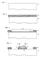
- an n-channel MOS IC is fabricated, in accordance with one embodiment of the invention, by forming a FOX 20 (i.e., a relatively thick layer 20 of SiO2) on a p-type silicon substrate 10 using, for example, conventional oxidation techniques.
- the doping level of the p-type dopant in the substrate 10 is, for example, 1x1015cm ⁇ 3.
- the thickness of the FOX 20 is, for example, 0.35 ⁇ m.
- the FOX 20 is now selectively etched using, for example, conventional lithographic and reactive ion etching (RIE) techniques, to expose regions 30 of the substrate surface, here termed GASAD (gate-and-source-and-drain) regions, where MOSFETs are to be formed.
- GASAD gate-and-source-and-drain regions
- a GOX 40 i.e., a relatively thin layer 40 of SiO2 having a thickness of, for example, 0.015 ⁇ m, is formed on the surface of the GASAD regions 30 using, for example, conventional oxidation techniques.
- the gate electrodes of the MOSFETs are formed by initially depositing a layer 50 of polycrystalline silicon (hereafter polysilicon) onto the GASAD regions 30, as well as onto the FOX 20.
- the deposition is carried out using, for example, conventional low pressure chemical vapor deposition (LPCVD) techniques, and the thickness of the deposited polysilicon is, for example, 0.3 ⁇ m.
- the polysilicon is made electrically conductive by implanting an n-type dopant, such as arsenic, into the polysilicon using an implant dose of, for example, 1x1015cm ⁇ 2, and ion energies of, for example, 80 keV.
- each sidewall of this structure forms an angle, ⁇ (see FIG. 4), relative to a perpendicular to the surface of the corresponding GASAD region, which is equal to or less than +15 degrees, and preferably zero degrees.
- ⁇ is positive when measured in the clockwise direction from the perpendicular.
- this angle is positive when measured in the counterclockwise direction.
- each gate electrode is formed to include a silicon dioxide sidewall spacer 55 (see FIG. 4) covering each polysilicon sidewall.
- a silicon-and-oxygen containing material such as tetraethyl orthosilicate (TEOS)
- TEOS is readily carried out using, for example, conventional LPCVD techniques, and the thickness of the TEOS is, for example, 0.1 ⁇ m.
- the TEOS is preferably heated to, for example, 900 degrees C for 20 minutes in a steam atmosphere in order to densify the TEOS and in effect convert it to a silicon dioxide-like material.
- the TEOS is then anisotropically etched, using, for example, RIE, in an etchant atmosphere of, for example, CHF3 and O2, in order to remove the TEOS from the FOX and GASAD surfaces, as well as from the upper surfaces of the polysilicon structures.
- RIE reactive etching
- a layer of metal capable of reacting with silicon to form a metal silicide such as titanium is deposited onto the upper surface of each polysilicon structure, onto the surfaces of the sidewall spacers 55, onto the exposed surfaces of the GASAD regions (where the sources and drains are to be formed) and onto the upper and sidewall surfaces of the FOX 20.
- the deposition is achieved using, for example, conventional sputtering techniques, and the thickness of the deposited titanium is, for example, 0.1 ⁇ m.
- the titanium-covered silicon substrate is heated, in a nitrogen (N2) atmosphere, to a temperature of about 600 degrees C for about 1 minute using conventional RTA techniques.
- this heating procedure results in the formation of successive layers of TiN, Ti and TiSi y , where y ⁇ 2.
- the above heating procedure results in the formation of successive layers of TiN and Ti.
- a selective wet etchant such as a solution of H2SO4:H2O2(1:1) heated to a temperature of 90 degrees C.
- TiSi2 - containing regions 60 and 70 see FIG.
- each polysilicon structure is formed on opposite sides of and vertically aligned with, and a TiSi2 - containing region 80 is formed on top of, each polysilicon structure, with each such region having a thickness of TiSi2 equal to about 0.08 ⁇ m.
- Each such region typically also includes a layer of TiN (a good electrical conductor), having a thickness of about 0.01 ⁇ m and overlying the TiSi2.)
- n+-type sources and drains one or more n-type dopants, e.g., arsenic ions or phosphorous ions, are implanted into the TiSi2- containing regions 60 and 70.
- the implant dose is, of course, chosen to satisfy the three conditions, discussed above.
- the ion energies are chosen so that essentially all the ions are implanted into the regions 60 and 70, and not into the underlying silicon.
- an interlevel dielectric 90 (see FIG. 6) is deposited onto the substrate.
- One such useful interlevel dielectric includes successive layers of undoped TEOS and phosphorus-doped TEOS, with the former having a thickness of, for example, 0.2 ⁇ m and the latter having a thickness of, for example, 0.8 ⁇ m.
- the upper surface of the deposited interlevel dielectric 90 is typically nonplanar (which is generally undesirable during subsequent processing).
- the substrate is heated.
- the temperature-time profile of the heating procedures is chosen to produce sources and drains having depths (as defined above) equal to or less than about 0.2 ⁇ m.
- the interlevel dielectric is patterned (using conventional techniques) to open via holes to the sources, drains and gate electrodes.
- Layers of material 120, 130 and 140 are now deposited onto the substrate and thus into the via holes extending, respectively, to the sources, drains, and gate electrodes, to serve as barriers to the (undesirable) interdiffusion of aluminum and silicon.
- These layers include, for example, a composite of 10 percent (by weight) titanium and 90 percent tungsten, and have thicknesses of, for example, 0.1 ⁇ m.
- a layer of aluminum having a thickness of, for example,1 ⁇ m is now deposited onto the interlevel dielectric 90, as well as onto the barrier layers 120, 130 and 140 in the via holes. Subsequent to deposition, the aluminum layer is patterned, using conventional techniques, to form interconnecting aluminum runners 150, 160 and 170 which terminate in metal contact pads.
- the n-channel MOS IC is completed by a series of conventional steps which typically includes the deposition of a silicon nitride layer onto the IC to form a barrier against moisture and mechanical damage.
- a CMOS IC is fabricated, in accordance with a second embodiment of the invention, by initially epitaxially growing a p-type silicon layer 210 (see FIG. 9) on a p+-type silicon substrate 200, using conventional techniques.
- the doping level of the substrate 200 is, for example, 1019cm ⁇ 3 while the doping level of the epitaxially grown layer 210 is, for example, 1015cm ⁇ 3.
- the thickness of the epitaxially grown layer 210 is, for example, 5 ⁇ m.
- Adjacent n- and p-tubs 240 and 250 are formed in the epitaxially grown layer 210 using the so-called twin-tub process described in U.S. Patent No. 4,435,896 issued to L. C. Parrillo and R. S. Payne on March 13, 1984. That is, a layer 220 of silicon nitride (see FIG. 10), having a thickness of, for example, 0.1 ⁇ m initially deposited onto the upper surface of the layer 210, using conventional deposition techniques. Conventional lithographic and RIE techniques are used to remove a portion of the silicon nitride layer 220, thus exposing the silicon surface of what is to become the n-tub 240.
- Donor ions e.g., phosphorus ions and arsenic ions
- the implant dose and energy for both phosphorus and arsenic ions being, for example, 2x1012cm ⁇ 2 and 100 keV, respectively.
- the silicon substrate is then heated in a steam-containing atmosphere to a temperature and for a corresponding heating time of, for example, 950 degrees C and 140 minutes, respectively, to form a layer 230 (see FIG. 10) of silicon dioxide having a thickness of about 0.4 ⁇ m, on the surface of the n-tub.
- the layer 220 of silicon nitride is now etched away with a wet etchant, such as hot H3PO4, and acceptor ions, e.g., boron ions, are implanted into the now exposed silicon surface of what is to become the p-tub 250.
- acceptor ions e.g., boron ions
- the silicon dioxide layer 230 shields the n-tub 240 from this implant.
- the implant dose and corresponding implant energy is, for example, 2x1012-cm ⁇ 2 and 50 keV, respectively.
- the silicon substrate is then heated in a nitrogen (N2) atmosphere to a temperature and for a corresponding time period of, for example, 1150 degrees C and 120 minutes, respectively to diffuse both the boron and phosphorus ions into the layer 210 to a depth of about 2 ⁇ m, thus forming both the n-tub 240 and p-tub 250 (see FIG. 11).
- N2 nitrogen
- the silicon dioxide layer 230 covering the n-tub 240 is etched away with a wet etchant, such as H2O:HF(7:1).
- a relatively thick layer 260 of silicon dioxide (see FIG. 12), having a thickness of, for example, 0.4 ⁇ m, which serves as the FOX in the CMOS IC, is now formed on the (now fully exposed) upper surface of the epitaxially grown layer 210. This is achieved by heating the silicon substrate in a high pressure steam-containing atmosphere, e.g., a steam-containing atmosphere exhibiting a pressure of 25 atmospheres, to a temperature and a corresponding heating time of, for example, 850 degrees C and 25 minutes, respectively.
- a high pressure steam-containing atmosphere e.g., a steam-containing atmosphere exhibiting a pressure of 25 atmospheres
- the relatively thick layer 260 of silicon dioxide is patterned, using conventional techniques, to expose GASAD regions 270 (see FIG. 12) on the surface of the p-tub 250, when n-channel MOSFETS are to be formed, and to expose GASAD regions 400 on the surface of the n-tub 240, where p-channel MOSFETs are to be formed.
- the silicon substrate is then heated to a temperature and for a corresponding time period of, for example, 900 degrees C and 27 minutes, respectively, to form layers 280 of silicon dioxide on the surfaces of the GASAD regions 270, and layers 410 of silicon dioxide on the surfaces of the GASAD regions 400, the layers 280 and 410 having thickness of about 0.0125 ⁇ m and serving as the GOXs of the n-channel and p-channel MOSFETs.
- the gate electrodes of the n-channel and p-channel MOSFETs are formed by initially depositing a layer of polysilicon having a thickness of, for example, 0.3 ⁇ m onto the GASAD regions 270 and 400, as well as onto the FOX 260.
- a photoresist is deposited onto the substrate and patterned to expose the substrate surface corresponding to the n-tub 240.
- Acceptor ions e.g., boron ions, are now implanted into the polysilicon overlying the n-tub, the resist shielding the polysilicon overlying the p-tub 250 from this implant.
- the implant dose and implant energy are, for example, 1x1015cm ⁇ 2 and 30 keV, respectively.
- the resist is stripped, and a second resist is deposited onto the substrate and patterned to expose the substrate surface corresponding to the p-tub 250.
- Donor ions e.g., arsenic ions
- the implant dose and implant energy corresponding to the donor ions are, for example 1x1015cm ⁇ 2 and 30 keV, respectively.
- the second resist is stripped, and the substrate is heated in a nitrogen (N2) atmosphere to a temperature and for a corresponding time period equal to, for example 900 degrees C and 30 minutes, respectively.
- the implanted dopants are diffused into the polysilicon, with the polysilicon overlying the n-tub 240 becoming of p-type conductivity, and the polysilicon overlying the n-tub 250 becoming of n-type conductivity.
- the deposited and implanted polysilicon (as well as the underlying, relatively thin layers 280 and 410 of silicon dioxide) are now patterned, as described above, to form polysilicon structures 290 and 420 (see FIG. 13) overlying, respectively, the GASAD regions 270 and 400.
- the sidewalls of these polysilicon structures must meet the requirement, discussed above.
- Silicon dioxide sidewall spacers 295 and 425 are formed on the polysilicon structures 290 and 420, respectively, as also described above.
- a layer of metal capable of reacting with silicon to form a metal silicide, such as cobalt, is deposited onto the upper surfaces of the polysilicon structures 290 and 420, onto the surfaces of the sidewall spacers 295 and 425, onto the exposed surfaces of the GASAD regions (where the sources and drains are to be formed) and onto the upper and sidewall surfaces of the FOX 260.
- the thickness of the deposited cobalt is, for example, .02 ⁇ m.
- the cobalt-covered substrate is heated in a reducing atmosphere, e.g., an atmosphere of H2, to a temperature and for a corresponding time period of, for example, 450 degrees C and ninety minutes, respectively.
- CoSi2 - containing regions 300 and 310 are formed on opposite sides of and vertically aligned with, and a CoSi2 - containing region 320 is formed on top of, each polysilicon structure 290.
- CoSi2 - containing regions 430 and 440 are formed on opposite sides of and vertically aligned with, and a CoSi2 - containing region 450 is formed on top of, each polysilicon structure 420.
- a photoresist having a thickness of, for example, 1 ⁇ m, is deposited onto the substrate, and then patterned to expose the surface of the n-tub.
- Acceptor ions are now implanted into the CoSi2-containing regions 430 and 440. (The resist serves to shield the p-tub 250 from this implant.)
- the implant dose is chosen to satisfy the three conditions, discussed above, while the ion energies are chosen so that essentially all the ions are implanted into the regions 430 and 440.
- the acceptor ions are, for example, boron ions, then it has been determined that a useful implant dose is 8x1015cm ⁇ 2, and that a useful, corresponding implant energy is 10 keV.
- the deposited and patterned photoresist is stripped, and another photoresist, also having a thickness of about 1 ⁇ m, is deposited onto the substrate and patterned, but this time to expose the surface of the p-tub 250.
- Donor ions are now implanted into the CoSi2-containing regions 300 and 310. (The newly-deposited resist serves to shield the n-tub 240 from this second implant.) Again, the implant dose and ion energies are chosen to satisfy the conditions and requirements dicussed above. In this regard, if the donor ions are, for example, arsenic ions, then it has been determined that a useful implant dose is 5x1015cm ⁇ 2, and a useful, corresponding implant energy is one which is equal to or less than 60 keV. On the other hand, if the donor ions are phosphorus ions, then a useful implant dose is 5x1015cm ⁇ 2, and a useful, corresponding implant energy is one which is equal to or less than 30 keV.
- an interlevel dielectric 600 including, for example, successive layers of 0.2 ⁇ m-thick undoped TEOS and 0.8 ⁇ m-thick phosphorus-doped TEOS, is deposited onto the substrate.
- the interlevel dielectric 600 is induced to flow, and the implanted dopants are diffused out the CoSi2-containing regions and into the underlying silicon to form CoSi2-covered n+-type sources and drains 330 and 340 (see FIG. 16) and CoSi2-covered p+-type sources and drains 460 and 470, by heating the substrate.
- a useful heating procedure is to heat the substrate to a temperature of 800 degrees C for 120 minutes.
- the heating temperatures employed when using furnace heating to fabricate the CMOS IC are less than 900 degrees C, and preferably equal to or less than about 850 degrees C.
- the interlevel dielectric 600 is patterned to open via holes to the sources, drains and gate electrodes. Barriers to the interdiffusion of aluminum and silicon, i.e., layers 350, 360, and 370 (see FIG. 17), and 480, 490, and 500, are deposited into the via holes. Interconnecting aluminum runners 375, 385, 395, and 505, 515, and 525 (see FIG. 17), extending form the sources, drains, and gate electrodes to metal contact pads, are formed, as described above.
- the CMOS IC is completed by a series of conventional steps which includes the deposition of a silicon nitride layer onto the IC to form a barrier against moisture and mechanical damage.
Landscapes
- Engineering & Computer Science (AREA)
- Microelectronics & Electronic Packaging (AREA)
- Power Engineering (AREA)
- Computer Hardware Design (AREA)
- Manufacturing & Machinery (AREA)
- Physics & Mathematics (AREA)
- Condensed Matter Physics & Semiconductors (AREA)
- General Physics & Mathematics (AREA)
- Ceramic Engineering (AREA)
- Electrodes Of Semiconductors (AREA)
- Insulated Gate Type Field-Effect Transistor (AREA)
- Metal-Oxide And Bipolar Metal-Oxide Semiconductor Integrated Circuits (AREA)
- Junction Field-Effect Transistors (AREA)
- Bipolar Transistors (AREA)
Applications Claiming Priority (2)
| Application Number | Priority Date | Filing Date | Title |
|---|---|---|---|
| US07/128,742 US4914500A (en) | 1987-12-04 | 1987-12-04 | Method for fabricating semiconductor devices which include sources and drains having metal-containing material regions, and the resulting devices |
| US128742 | 1987-12-04 |
Publications (2)
| Publication Number | Publication Date |
|---|---|
| EP0319213A2 true EP0319213A2 (de) | 1989-06-07 |
| EP0319213A3 EP0319213A3 (de) | 1989-12-06 |
Family
ID=22436758
Family Applications (1)
| Application Number | Title | Priority Date | Filing Date |
|---|---|---|---|
| EP88311213A Withdrawn EP0319213A3 (de) | 1987-12-04 | 1988-11-25 | Verfahren zur Herstellung von Halbleiteranordnungen, umfassend Metall enthaltende Materialgebiete |
Country Status (5)
| Country | Link |
|---|---|
| US (1) | US4914500A (de) |
| EP (1) | EP0319213A3 (de) |
| JP (1) | JP2769169B2 (de) |
| KR (1) | KR920010131B1 (de) |
| CA (1) | CA1289269C (de) |
Cited By (5)
| Publication number | Priority date | Publication date | Assignee | Title |
|---|---|---|---|---|
| EP0543223A2 (de) * | 1991-11-12 | 1993-05-26 | Siemens Aktiengesellschaft | Verfahren zur Bildung von flachen Übergängen für Feldeffekttransistoren |
| EP0671759A2 (de) * | 1994-03-09 | 1995-09-13 | Siemens Aktiengesellschaft | MOSFETs mit niedrigen Übergangsverlusten |
| GB2299209A (en) * | 1995-03-24 | 1996-09-25 | Nec Corp | Process for fabricating a semiconductor device |
| EP0813234A2 (de) * | 1996-06-12 | 1997-12-17 | Texas Instruments Incorporated | Verfahren zur Herstellung eines MOSFETS |
| EP0929105A2 (de) * | 1998-01-09 | 1999-07-14 | Sharp Kabushiki Kaisha | Metalgate-Submikron-MOS-Transistor und Verfahren zur Hertellung |
Families Citing this family (41)
| Publication number | Priority date | Publication date | Assignee | Title |
|---|---|---|---|---|
| US5570119A (en) * | 1988-07-26 | 1996-10-29 | Canon Kabushiki Kaisha | Multilayer device having integral functional element for use with an ink jet recording apparatus, and recording apparatus |
| JPH06105726B2 (ja) * | 1989-10-13 | 1994-12-21 | 三菱電機株式会社 | 半導体集積回路装置 |
| JP2662446B2 (ja) * | 1989-12-11 | 1997-10-15 | キヤノン株式会社 | 記録ヘッド及び記録ヘッド用素子基板 |
| DK170189B1 (da) * | 1990-05-30 | 1995-06-06 | Yakov Safir | Fremgangsmåde til fremstilling af halvlederkomponenter, samt solcelle fremstillet deraf |
| US5403760A (en) * | 1990-10-16 | 1995-04-04 | Texas Instruments Incorporated | Method of making a HgCdTe thin film transistor |
| KR950013785B1 (ko) * | 1991-01-21 | 1995-11-16 | 미쓰비시 뎅끼 가부시끼가이샤 | Mos형 전계효과 트랜지스터를 포함하는 반도체장치 및 그 제조방법 |
| US5086017A (en) * | 1991-03-21 | 1992-02-04 | Industrial Technology Research Institute | Self aligned silicide process for gate/runner without extra masking |
| JP3277533B2 (ja) * | 1992-01-08 | 2002-04-22 | ソニー株式会社 | 半導体装置の製造方法 |
| JP3199847B2 (ja) * | 1992-07-09 | 2001-08-20 | 株式会社東芝 | 半導体装置およびその製造方法 |
| US5316969A (en) * | 1992-12-21 | 1994-05-31 | Board Of Trustees Of The Leland Stanford Junior University | Method of shallow junction formation in semiconductor devices using gas immersion laser doping |
| JP3514500B2 (ja) * | 1994-01-28 | 2004-03-31 | 株式会社ルネサステクノロジ | 半導体装置及びその製造方法 |
| US5536684A (en) * | 1994-06-30 | 1996-07-16 | Intel Corporation | Process for formation of epitaxial cobalt silicide and shallow junction of silicon |
| JPH08148561A (ja) * | 1994-11-16 | 1996-06-07 | Mitsubishi Electric Corp | 半導体装置とその製造方法 |
| US5646435A (en) * | 1995-04-04 | 1997-07-08 | Taiwan Semiconductor Manufacturing Company, Ltd. | Method for fabricating CMOS field effect transistors having sub-quarter micrometer channel lengths with improved short channel effect characteristics |
| US6969671B2 (en) * | 1995-11-14 | 2005-11-29 | Renesas Technology Corporation | Semiconductor integrated device and method of fabrication thereof |
| JP3443219B2 (ja) | 1995-11-14 | 2003-09-02 | 株式会社日立製作所 | 半導体集積回路装置およびその製造方法 |
| US6303446B1 (en) * | 1996-01-29 | 2001-10-16 | The Regents Of The University Of California | Method of making self-aligned lightly-doped-drain structure for MOS transistors |
| SE9601174D0 (sv) * | 1996-03-27 | 1996-03-27 | Abb Research Ltd | A method for producing a semiconductor device having a semiconductor layer of SiC and such a device |
| JP4142753B2 (ja) * | 1996-12-26 | 2008-09-03 | 株式会社東芝 | スパッタターゲット、スパッタ装置、半導体装置およびその製造方法 |
| US6093967A (en) * | 1997-12-17 | 2000-07-25 | Advanced Micro Devices, Inc. | Self-aligned silicide contacts formed from deposited silicon |
| US6140230A (en) * | 1998-02-19 | 2000-10-31 | Micron Technology, Inc. | Methods of forming metal nitride and silicide structures |
| WO2000017918A1 (en) * | 1998-09-21 | 2000-03-30 | The Penn State Research Foundation | Metal-contact induced crystallization in semiconductor devices |
| US6268285B1 (en) * | 1999-01-04 | 2001-07-31 | Advanced Micro Devices, Inc. | Method of removing plasma etch damage to pre-silicidized surfaces by wet silicon etch |
| JP3403115B2 (ja) * | 1999-04-02 | 2003-05-06 | シャープ株式会社 | 半導体装置の製造方法 |
| KR100341182B1 (ko) * | 1999-11-30 | 2002-06-20 | 윤종용 | 반도체소자의 모스 트랜지스터 형성방법 |
| US7294563B2 (en) * | 2000-08-10 | 2007-11-13 | Applied Materials, Inc. | Semiconductor on insulator vertical transistor fabrication and doping process |
| US6893907B2 (en) * | 2002-06-05 | 2005-05-17 | Applied Materials, Inc. | Fabrication of silicon-on-insulator structure using plasma immersion ion implantation |
| US6846729B2 (en) * | 2001-10-01 | 2005-01-25 | International Rectifier Corporation | Process for counter doping N-type silicon in Schottky device Ti silicide barrier |
| JP2004055803A (ja) * | 2002-07-19 | 2004-02-19 | Renesas Technology Corp | 半導体装置 |
| US7084423B2 (en) | 2002-08-12 | 2006-08-01 | Acorn Technologies, Inc. | Method for depinning the Fermi level of a semiconductor at an electrical junction and devices incorporating such junctions |
| US6833556B2 (en) | 2002-08-12 | 2004-12-21 | Acorn Technologies, Inc. | Insulated gate field effect transistor having passivated schottky barriers to the channel |
| US7625603B2 (en) * | 2003-11-14 | 2009-12-01 | Robert Bosch Gmbh | Crack and residue free conformal deposited silicon oxide with predictable and uniform etching characteristics |
| US7193228B2 (en) * | 2004-03-10 | 2007-03-20 | Cymer, Inc. | EUV light source optical elements |
| US8280719B2 (en) * | 2005-05-05 | 2012-10-02 | Ramp, Inc. | Methods and systems relating to information extraction |
| US7288828B2 (en) * | 2005-10-05 | 2007-10-30 | United Microelectronics Corp. | Metal oxide semiconductor transistor device |
| JP4935111B2 (ja) * | 2006-02-22 | 2012-05-23 | 富士通株式会社 | 絶縁膜形成用組成物、半導体装置用絶縁膜、その製造方法および半導体装置 |
| US8258057B2 (en) * | 2006-03-30 | 2012-09-04 | Intel Corporation | Copper-filled trench contact for transistor performance improvement |
| DE112012004882B4 (de) | 2011-11-23 | 2022-12-29 | Acorn Technologies, Inc. | Verbesserung von Metallkontakten zu Gruppe-IV-Halbleitern durch Einfügung grenzflächiger atomischer Monoschichten |
| KR20160058499A (ko) | 2014-11-17 | 2016-05-25 | 삼성전자주식회사 | 반도체 소자, 및 그 반도체 소자의 제조방법과 제조장치 |
| US9620611B1 (en) | 2016-06-17 | 2017-04-11 | Acorn Technology, Inc. | MIS contact structure with metal oxide conductor |
| DE112017005855T5 (de) | 2016-11-18 | 2019-08-01 | Acorn Technologies, Inc. | Nanodrahttransistor mit Source und Drain induziert durch elektrische Kontakte mit negativer Schottky-Barrierenhöhe |
Family Cites Families (8)
| Publication number | Priority date | Publication date | Assignee | Title |
|---|---|---|---|---|
| US4378628A (en) * | 1981-08-27 | 1983-04-05 | Bell Telephone Laboratories, Incorporated | Cobalt silicide metallization for semiconductor integrated circuits |
| JPS59151422A (ja) * | 1983-02-18 | 1984-08-29 | Nec Corp | 浅い接合を有する半導体装置の製造方法 |
| KR910006249B1 (ko) * | 1983-04-01 | 1991-08-17 | 가부시기가이샤 히다찌세이사꾸쇼 | 반도체 장치 |
| JPS60198814A (ja) * | 1984-03-23 | 1985-10-08 | Nec Corp | 半導体装置の製造方法 |
| US4697198A (en) * | 1984-08-22 | 1987-09-29 | Hitachi, Ltd. | MOSFET which reduces the short-channel effect |
| JPS61248476A (ja) * | 1985-04-26 | 1986-11-05 | Hitachi Ltd | 半導体装置の製造方法 |
| JPS6239051A (ja) * | 1985-08-14 | 1987-02-20 | Toshiba Corp | 半導体装置の製造方法 |
| US4689869A (en) * | 1986-04-07 | 1987-09-01 | International Business Machines Corporation | Fabrication of insulated gate gallium arsenide FET with self-aligned source/drain and submicron channel length |
-
1987
- 1987-12-04 US US07/128,742 patent/US4914500A/en not_active Expired - Lifetime
-
1988
- 1988-11-25 EP EP88311213A patent/EP0319213A3/de not_active Withdrawn
- 1988-12-02 KR KR1019880016051A patent/KR920010131B1/ko not_active IP Right Cessation
- 1988-12-02 CA CA000584850A patent/CA1289269C/en not_active Expired - Lifetime
- 1988-12-05 JP JP63306210A patent/JP2769169B2/ja not_active Expired - Lifetime
Non-Patent Citations (8)
| Title |
|---|
| 1986 Symposium on VLSI Technology; Digest of Technical Papers, San Diego, 28th-30th May 1986, pages 49-50; N. KOBAYASHI et al.: "Comparison of TiSi2 and WSi2 silicided shallow junctions for sub-micron CMOSs" * |
| Extended Abstracts, Vol. 87-1, No. 1, Spring 1987, pages 216-217, Abstract No. 156, Philadelphia, PA, US; B. DAVARI et al.: "Very shallow junctions for submicron CMOS technology using implanted Ti for silidation" * |
| IBM Journal of Research & Development, Vol. 31, No. 6, November 1987, pages 627-633, New York, US; Y. TAUR et al.: "Study of contact and shallow junction characteristics in submicron CMOS with self-aligned titanium silicide" * |
| IEEE Transactions on Electron Devices, Vol. ED-33, No. 2, February 1986, pages 260-269, IEEE, New York, US; M. HORIUCHI et al.: "Solid-II: High-voltage high-gain kilo-Angstrom-channel-length CMOSFET's using silicide with self-aligned utrashallow (3S) junction" * |
| IEEE Transactions on Electron Devices, Vol. ED-34, No. 3, March 1987, pages 575-580, IEEE, New York, NY, US; Y. TAUR et al.: "Source-drain contact resistance in CMOS with self-aligned TiSi2" * |
| International Electron Devices Meeting, Los Angeles, 7th-10th December 1986, pages 58-61, IEEE, New York, US; R. LIU et al.: "Mechanisms for process-induced leakage in shallow silicided junctions" * |
| International Electron Devices Meeting, Washington, DC, 1st-4th December 1985, pages 407-410, IEEE, New York, US; F.C. SHONE et al.: "Formation of 0.1 mum N+/P and P+/N junctions by doped silicide technology". * |
| Japanese Journal of Applied Physics - 17th Conference on Solid State Devices and Materials, 25th-27th August 1985, pages 325-328, Tokyo, JP; N. NATSUAKI et al.: "Refractory-metal-silicide contact formation by rapid thermal annealing" * |
Cited By (12)
| Publication number | Priority date | Publication date | Assignee | Title |
|---|---|---|---|---|
| EP0543223A2 (de) * | 1991-11-12 | 1993-05-26 | Siemens Aktiengesellschaft | Verfahren zur Bildung von flachen Übergängen für Feldeffekttransistoren |
| EP0543223A3 (en) * | 1991-11-12 | 1996-07-17 | Siemens Ag | Method of forming shallow junctions in field effect transistors |
| EP0671759A2 (de) * | 1994-03-09 | 1995-09-13 | Siemens Aktiengesellschaft | MOSFETs mit niedrigen Übergangsverlusten |
| EP0671759A3 (de) * | 1994-03-09 | 1996-07-17 | Siemens Ag | MOSFETs mit niedrigen Übergangsverlusten. |
| GB2299209A (en) * | 1995-03-24 | 1996-09-25 | Nec Corp | Process for fabricating a semiconductor device |
| US5770494A (en) * | 1995-03-24 | 1998-06-23 | Nec Corporation | Process of fabricating semiconductor device having gate structure doped through diffusion from refractory metal silicide into polysilicon |
| GB2299209B (en) * | 1995-03-24 | 1999-05-19 | Nec Corp | Process for fabricating a semiconductor device |
| EP0813234A2 (de) * | 1996-06-12 | 1997-12-17 | Texas Instruments Incorporated | Verfahren zur Herstellung eines MOSFETS |
| EP0813234A3 (de) * | 1996-06-12 | 1999-05-26 | Texas Instruments Incorporated | Verfahren zur Herstellung eines MOSFETS |
| EP0929105A2 (de) * | 1998-01-09 | 1999-07-14 | Sharp Kabushiki Kaisha | Metalgate-Submikron-MOS-Transistor und Verfahren zur Hertellung |
| EP0929105A3 (de) * | 1998-01-09 | 1999-12-22 | Sharp Kabushiki Kaisha | Metalgate-Submikron-MOS-Transistor und Verfahren zur Hertellung |
| US6274421B1 (en) | 1998-01-09 | 2001-08-14 | Sharp Laboratories Of America, Inc. | Method of making metal gate sub-micron MOS transistor |
Also Published As
| Publication number | Publication date |
|---|---|
| US4914500A (en) | 1990-04-03 |
| JP2769169B2 (ja) | 1998-06-25 |
| CA1289269C (en) | 1991-09-17 |
| KR920010131B1 (ko) | 1992-11-16 |
| JPH021944A (ja) | 1990-01-08 |
| EP0319213A3 (de) | 1989-12-06 |
| KR890011074A (ko) | 1989-08-12 |
Similar Documents
| Publication | Publication Date | Title |
|---|---|---|
| US4914500A (en) | Method for fabricating semiconductor devices which include sources and drains having metal-containing material regions, and the resulting devices | |
| US7091093B1 (en) | Method for fabricating a semiconductor device having a pocket dopant diffused layer | |
| EP0091775B1 (de) | Verfahren zum Herstellen einer Halbleiteranordnung mit einer Verbindungsschicht | |
| US5428240A (en) | Source/drain structural configuration for MOSFET integrated circuit devices | |
| US6225176B1 (en) | Step drain and source junction formation | |
| US5169794A (en) | Method of fabrication of pnp structure in a common substrate containing npn or MOS structures | |
| US6069398A (en) | Thin film resistor and fabrication method thereof | |
| US6184097B1 (en) | Process for forming ultra-shallow source/drain extensions | |
| US5661046A (en) | Method of fabricating BiCMOS device | |
| US5103272A (en) | Semiconductor device and a method for manufacturing the same | |
| EP0118513B1 (de) | Verfahren zum herstellen einer cmos-struktur | |
| US5908309A (en) | Fabrication method of semiconductor device with CMOS structure | |
| EP1253632A2 (de) | Neuer Tansistor mit einer ultraflachen Zone und Verfahren zur Herstellung | |
| US5780350A (en) | MOSFET device with improved LDD region and method of making same | |
| US6096591A (en) | Method of making an IGFET and a protected resistor with reduced processing steps | |
| US5918130A (en) | Transistor fabrication employing formation of silicide across source and drain regions prior to formation of the gate conductor | |
| US4471524A (en) | Method for manufacturing an insulated gate field effect transistor device | |
| US6555453B1 (en) | Fully nickel silicided metal gate with shallow junction formed | |
| US5107321A (en) | Interconnect method for semiconductor devices | |
| US6518625B1 (en) | Semiconductor device | |
| EP1011129A2 (de) | Verfahren zur Herstellung von einem Halbleiterbauelement | |
| US5801086A (en) | Process for formation of contact conductive layer in a semiconductor device | |
| JPH05326552A (ja) | 半導体素子およびその製造方法 | |
| US5885874A (en) | Method of making enhancement-mode and depletion-mode IGFETS using selective doping of a gate material | |
| US6163059A (en) | Integrated circuit including source implant self-aligned to contact via |
Legal Events
| Date | Code | Title | Description |
|---|---|---|---|
| PUAI | Public reference made under article 153(3) epc to a published international application that has entered the european phase |
Free format text: ORIGINAL CODE: 0009012 |
|
| AK | Designated contracting states |
Kind code of ref document: A2 Designated state(s): DE ES FR GB NL |
|
| PUAL | Search report despatched |
Free format text: ORIGINAL CODE: 0009013 |
|
| AK | Designated contracting states |
Kind code of ref document: A3 Designated state(s): DE ES FR GB NL |
|
| 17P | Request for examination filed |
Effective date: 19900515 |
|
| 17Q | First examination report despatched |
Effective date: 19920415 |
|
| RAP3 | Party data changed (applicant data changed or rights of an application transferred) |
Owner name: AT&T CORP. |
|
| APCB | Communication from the board of appeal sent |
Free format text: ORIGINAL CODE: EPIDOS OBAPE |
|
| APCB | Communication from the board of appeal sent |
Free format text: ORIGINAL CODE: EPIDOS OBAPE |
|
| APAB | Appeal dossier modified |
Free format text: ORIGINAL CODE: EPIDOS NOAPE |
|
| STAA | Information on the status of an ep patent application or granted ep patent |
Free format text: STATUS: THE APPLICATION IS DEEMED TO BE WITHDRAWN |
|
| 18D | Application deemed to be withdrawn |
Effective date: 19970301 |
|
| APAF | Appeal reference modified |
Free format text: ORIGINAL CODE: EPIDOSCREFNE |