US5316969A - Method of shallow junction formation in semiconductor devices using gas immersion laser doping - Google Patents
Method of shallow junction formation in semiconductor devices using gas immersion laser doping Download PDFInfo
- Publication number
- US5316969A US5316969A US07/993,788 US99378892A US5316969A US 5316969 A US5316969 A US 5316969A US 99378892 A US99378892 A US 99378892A US 5316969 A US5316969 A US 5316969A
- Authority
- US
- United States
- Prior art keywords
- dopant
- silicide layer
- semiconductor body
- silicide
- atoms
- Prior art date
- Legal status (The legal status is an assumption and is not a legal conclusion. Google has not performed a legal analysis and makes no representation as to the accuracy of the status listed.)
- Expired - Lifetime
Links
- 239000004065 semiconductor Substances 0.000 title claims abstract description 24
- 238000000034 method Methods 0.000 title claims description 32
- 238000007654 immersion Methods 0.000 title description 6
- 230000015572 biosynthetic process Effects 0.000 title description 2
- 239000002019 doping agent Substances 0.000 claims abstract description 43
- 229910021332 silicide Inorganic materials 0.000 claims abstract description 34
- FVBUAEGBCNSCDD-UHFFFAOYSA-N silicide(4-) Chemical compound [Si-4] FVBUAEGBCNSCDD-UHFFFAOYSA-N 0.000 claims abstract description 31
- 239000000463 material Substances 0.000 claims abstract description 12
- 230000001678 irradiating effect Effects 0.000 claims abstract 7
- 229910052710 silicon Inorganic materials 0.000 claims description 13
- 239000010703 silicon Substances 0.000 claims description 13
- 230000000873 masking effect Effects 0.000 claims description 9
- 238000002844 melting Methods 0.000 claims description 6
- 230000008018 melting Effects 0.000 claims description 6
- WQJQOUPTWCFRMM-UHFFFAOYSA-N tungsten disilicide Chemical compound [Si]#[W]#[Si] WQJQOUPTWCFRMM-UHFFFAOYSA-N 0.000 claims description 5
- 229910021342 tungsten silicide Inorganic materials 0.000 claims description 5
- 229910052782 aluminium Inorganic materials 0.000 claims description 3
- XAGFODPZIPBFFR-UHFFFAOYSA-N aluminium Chemical compound [Al] XAGFODPZIPBFFR-UHFFFAOYSA-N 0.000 claims description 3
- 229910021420 polycrystalline silicon Inorganic materials 0.000 claims description 3
- 230000005855 radiation Effects 0.000 claims 3
- 239000007789 gas Substances 0.000 description 24
- 239000000523 sample Substances 0.000 description 11
- XUIMIQQOPSSXEZ-UHFFFAOYSA-N Silicon Chemical compound [Si] XUIMIQQOPSSXEZ-UHFFFAOYSA-N 0.000 description 10
- 239000000758 substrate Substances 0.000 description 7
- ZOXJGFHDIHLPTG-UHFFFAOYSA-N Boron Chemical compound [B] ZOXJGFHDIHLPTG-UHFFFAOYSA-N 0.000 description 6
- 229910052796 boron Inorganic materials 0.000 description 4
- 238000000137 annealing Methods 0.000 description 3
- 238000009792 diffusion process Methods 0.000 description 3
- 238000010849 ion bombardment Methods 0.000 description 3
- 229910052698 phosphorus Inorganic materials 0.000 description 3
- IJGRMHOSHXDMSA-UHFFFAOYSA-N Atomic nitrogen Chemical compound N#N IJGRMHOSHXDMSA-UHFFFAOYSA-N 0.000 description 2
- 206010033296 Overdoses Diseases 0.000 description 2
- OAICVXFJPJFONN-UHFFFAOYSA-N Phosphorus Chemical compound [P] OAICVXFJPJFONN-UHFFFAOYSA-N 0.000 description 2
- 229910008814 WSi2 Inorganic materials 0.000 description 2
- QVGXLLKOCUKJST-UHFFFAOYSA-N atomic oxygen Chemical compound [O] QVGXLLKOCUKJST-UHFFFAOYSA-N 0.000 description 2
- 238000004140 cleaning Methods 0.000 description 2
- 238000005468 ion implantation Methods 0.000 description 2
- 239000000155 melt Substances 0.000 description 2
- 229910052751 metal Inorganic materials 0.000 description 2
- 239000002184 metal Substances 0.000 description 2
- 238000012986 modification Methods 0.000 description 2
- 230000004048 modification Effects 0.000 description 2
- 239000001301 oxygen Substances 0.000 description 2
- 229910052760 oxygen Inorganic materials 0.000 description 2
- 239000011574 phosphorus Substances 0.000 description 2
- 238000002310 reflectometry Methods 0.000 description 2
- 229910003556 H2 SO4 Inorganic materials 0.000 description 1
- 238000003917 TEM image Methods 0.000 description 1
- 238000004458 analytical method Methods 0.000 description 1
- 229910052785 arsenic Inorganic materials 0.000 description 1
- RQNWIZPPADIBDY-UHFFFAOYSA-N arsenic atom Chemical compound [As] RQNWIZPPADIBDY-UHFFFAOYSA-N 0.000 description 1
- 229910052792 caesium Inorganic materials 0.000 description 1
- TVFDJXOCXUVLDH-UHFFFAOYSA-N caesium atom Chemical compound [Cs] TVFDJXOCXUVLDH-UHFFFAOYSA-N 0.000 description 1
- 229910001417 caesium ion Inorganic materials 0.000 description 1
- 238000003486 chemical etching Methods 0.000 description 1
- 229910017052 cobalt Inorganic materials 0.000 description 1
- 239000010941 cobalt Substances 0.000 description 1
- GUTLYIVDDKVIGB-UHFFFAOYSA-N cobalt atom Chemical compound [Co] GUTLYIVDDKVIGB-UHFFFAOYSA-N 0.000 description 1
- 238000010438 heat treatment Methods 0.000 description 1
- 238000013383 initial experiment Methods 0.000 description 1
- 238000004518 low pressure chemical vapour deposition Methods 0.000 description 1
- 238000004519 manufacturing process Methods 0.000 description 1
- 239000011159 matrix material Substances 0.000 description 1
- 150000002739 metals Chemical class 0.000 description 1
- 229910052757 nitrogen Inorganic materials 0.000 description 1
- 229920002120 photoresistant polymer Polymers 0.000 description 1
- 238000004886 process control Methods 0.000 description 1
- 238000007788 roughening Methods 0.000 description 1
- 238000005389 semiconductor device fabrication Methods 0.000 description 1
- 238000001228 spectrum Methods 0.000 description 1
- 229910052721 tungsten Inorganic materials 0.000 description 1
Images


Classifications
-
- H—ELECTRICITY
- H01—ELECTRIC ELEMENTS
- H01L—SEMICONDUCTOR DEVICES NOT COVERED BY CLASS H10
- H01L21/00—Processes or apparatus adapted for the manufacture or treatment of semiconductor or solid state devices or of parts thereof
- H01L21/67—Apparatus specially adapted for handling semiconductor or electric solid state devices during manufacture or treatment thereof; Apparatus specially adapted for handling wafers during manufacture or treatment of semiconductor or electric solid state devices or components ; Apparatus not specifically provided for elsewhere
- H01L21/67005—Apparatus not specifically provided for elsewhere
- H01L21/67242—Apparatus for monitoring, sorting or marking
- H01L21/67253—Process monitoring, e.g. flow or thickness monitoring
-
- H—ELECTRICITY
- H01—ELECTRIC ELEMENTS
- H01L—SEMICONDUCTOR DEVICES NOT COVERED BY CLASS H10
- H01L21/00—Processes or apparatus adapted for the manufacture or treatment of semiconductor or solid state devices or of parts thereof
- H01L21/02—Manufacture or treatment of semiconductor devices or of parts thereof
- H01L21/04—Manufacture or treatment of semiconductor devices or of parts thereof the devices having potential barriers, e.g. a PN junction, depletion layer or carrier concentration layer
- H01L21/18—Manufacture or treatment of semiconductor devices or of parts thereof the devices having potential barriers, e.g. a PN junction, depletion layer or carrier concentration layer the devices having semiconductor bodies comprising elements of Group IV of the Periodic Table or AIIIBV compounds with or without impurities, e.g. doping materials
- H01L21/22—Diffusion of impurity materials, e.g. doping materials, electrode materials, into or out of a semiconductor body, or between semiconductor regions; Interactions between two or more impurities; Redistribution of impurities
- H01L21/223—Diffusion of impurity materials, e.g. doping materials, electrode materials, into or out of a semiconductor body, or between semiconductor regions; Interactions between two or more impurities; Redistribution of impurities using diffusion into or out of a solid from or into a gaseous phase
-
- H—ELECTRICITY
- H01—ELECTRIC ELEMENTS
- H01L—SEMICONDUCTOR DEVICES NOT COVERED BY CLASS H10
- H01L21/00—Processes or apparatus adapted for the manufacture or treatment of semiconductor or solid state devices or of parts thereof
- H01L21/02—Manufacture or treatment of semiconductor devices or of parts thereof
- H01L21/04—Manufacture or treatment of semiconductor devices or of parts thereof the devices having potential barriers, e.g. a PN junction, depletion layer or carrier concentration layer
- H01L21/18—Manufacture or treatment of semiconductor devices or of parts thereof the devices having potential barriers, e.g. a PN junction, depletion layer or carrier concentration layer the devices having semiconductor bodies comprising elements of Group IV of the Periodic Table or AIIIBV compounds with or without impurities, e.g. doping materials
- H01L21/22—Diffusion of impurity materials, e.g. doping materials, electrode materials, into or out of a semiconductor body, or between semiconductor regions; Interactions between two or more impurities; Redistribution of impurities
- H01L21/225—Diffusion of impurity materials, e.g. doping materials, electrode materials, into or out of a semiconductor body, or between semiconductor regions; Interactions between two or more impurities; Redistribution of impurities using diffusion into or out of a solid from or into a solid phase, e.g. a doped oxide layer
- H01L21/2251—Diffusion into or out of group IV semiconductors
- H01L21/2252—Diffusion into or out of group IV semiconductors using predeposition of impurities into the semiconductor surface, e.g. from a gaseous phase
-
- H—ELECTRICITY
- H01—ELECTRIC ELEMENTS
- H01L—SEMICONDUCTOR DEVICES NOT COVERED BY CLASS H10
- H01L21/00—Processes or apparatus adapted for the manufacture or treatment of semiconductor or solid state devices or of parts thereof
- H01L21/02—Manufacture or treatment of semiconductor devices or of parts thereof
- H01L21/04—Manufacture or treatment of semiconductor devices or of parts thereof the devices having potential barriers, e.g. a PN junction, depletion layer or carrier concentration layer
- H01L21/18—Manufacture or treatment of semiconductor devices or of parts thereof the devices having potential barriers, e.g. a PN junction, depletion layer or carrier concentration layer the devices having semiconductor bodies comprising elements of Group IV of the Periodic Table or AIIIBV compounds with or without impurities, e.g. doping materials
- H01L21/22—Diffusion of impurity materials, e.g. doping materials, electrode materials, into or out of a semiconductor body, or between semiconductor regions; Interactions between two or more impurities; Redistribution of impurities
- H01L21/225—Diffusion of impurity materials, e.g. doping materials, electrode materials, into or out of a semiconductor body, or between semiconductor regions; Interactions between two or more impurities; Redistribution of impurities using diffusion into or out of a solid from or into a solid phase, e.g. a doped oxide layer
- H01L21/2251—Diffusion into or out of group IV semiconductors
- H01L21/2254—Diffusion into or out of group IV semiconductors from or through or into an applied layer, e.g. photoresist, nitrides
- H01L21/2257—Diffusion into or out of group IV semiconductors from or through or into an applied layer, e.g. photoresist, nitrides the applied layer being silicon or silicide or SIPOS, e.g. polysilicon, porous silicon
-
- H—ELECTRICITY
- H01—ELECTRIC ELEMENTS
- H01L—SEMICONDUCTOR DEVICES NOT COVERED BY CLASS H10
- H01L21/00—Processes or apparatus adapted for the manufacture or treatment of semiconductor or solid state devices or of parts thereof
- H01L21/02—Manufacture or treatment of semiconductor devices or of parts thereof
- H01L21/04—Manufacture or treatment of semiconductor devices or of parts thereof the devices having potential barriers, e.g. a PN junction, depletion layer or carrier concentration layer
- H01L21/18—Manufacture or treatment of semiconductor devices or of parts thereof the devices having potential barriers, e.g. a PN junction, depletion layer or carrier concentration layer the devices having semiconductor bodies comprising elements of Group IV of the Periodic Table or AIIIBV compounds with or without impurities, e.g. doping materials
- H01L21/30—Treatment of semiconductor bodies using processes or apparatus not provided for in groups H01L21/20 - H01L21/26
- H01L21/31—Treatment of semiconductor bodies using processes or apparatus not provided for in groups H01L21/20 - H01L21/26 to form insulating layers thereon, e.g. for masking or by using photolithographic techniques; After treatment of these layers; Selection of materials for these layers
- H01L21/3205—Deposition of non-insulating-, e.g. conductive- or resistive-, layers on insulating layers; After-treatment of these layers
- H01L21/321—After treatment
- H01L21/3215—Doping the layers
- H01L21/32155—Doping polycristalline - or amorphous silicon layers
-
- Y—GENERAL TAGGING OF NEW TECHNOLOGICAL DEVELOPMENTS; GENERAL TAGGING OF CROSS-SECTIONAL TECHNOLOGIES SPANNING OVER SEVERAL SECTIONS OF THE IPC; TECHNICAL SUBJECTS COVERED BY FORMER USPC CROSS-REFERENCE ART COLLECTIONS [XRACs] AND DIGESTS
- Y10—TECHNICAL SUBJECTS COVERED BY FORMER USPC
- Y10S—TECHNICAL SUBJECTS COVERED BY FORMER USPC CROSS-REFERENCE ART COLLECTIONS [XRACs] AND DIGESTS
- Y10S148/00—Metal treatment
- Y10S148/129—Pulse doping
Definitions
- This invention relates generally to semiconductor device fabrication, and more particularly the invention relates to the formation of shallow junctions in a semiconductor device through the selective introduction of dopants.
- Semiconductor devices and integrated circuits are fabricated through the selective introduction of dopant atoms into a semiconductor substrate.
- photoresist masking and chemical etching techniques are utilized to define diffusion windows for the dopant atom diffusion or ion implantation into the wafer.
- shallower junctions are needed in the device structures.
- One method of obtaining shallow junctions is to outdiffuse dopants from a doped silicide layer into the underlying substrate using rapid thermal lamp annealing.
- the use of silicides minimizes contact and series resistances and prevents damage to the underlying silicon. Shorting problems which are encountered in the silicidation of preformed shallow junctions are prevented since the dopant profile in the silicon substrate follows the contour of the silicide/silicon interface.
- Rapid thermal lamp annealing typically has a relatively long heat cycle (e.g., seconds) which limits the amount of dopant in shallow junction devices. Further, the entire wafer is heated, which can lead to warpage. Pulsed laser techniques have been introduced to overcome these limitations.
- gas immersion laser doping a suitably masked wafer of a semiconductor such as silicon is placed in a gas cell and immersed in a desired dopant gas such as BF 3 , ASF 5 , and PF 5 / A pulsed, high-intensity laser is then used to heat the masked wafer with dopant atoms being driven into a shallow silicon surface region during a melt/regrowth of the exposed silicon surface.
- the present invention modifies the gas immersion laser doping process to provide shallower junctions and better process control and less dopant per pulse along with less disruption of existing doped regions.
- a semiconductor wafer is immersed in a dopant gas and heated by a pulsed laser so that the wafer does not melt but dopant atoms are adsorbed on the surface prior to laser irradiation and diffused into the surface during irradiation. Since only a surface region is heated, selected doping of device areas is achieved.
- the pulsed laser has a short rise time during which dopants can desorb from the surface and allows dopants to be replenished onto the surface while the laser is off.
- the non-melt doping can be followed by a standard GILD process with melting to form shallow, square junctions.
- the surface of the wafer can be covered by a silicide layer, and the dopant is diffused through the silicide into the surface region of the wafer. Since dopant diffusion coefficients in silicides are very large, melting of the silicide is not required to incorporate the dopant or to drive dopant into the film/substrate interface.
- dopant can be concentrated in the silicide layer, and the laser outdiffuses the dopant atoms into the semiconductor surface regions.
- FIG. 1 is a schematic of a gas immersion laser doping apparatus.
- FIG. 2 is a graph illustrating SIMS results from a non-melt sample in accordance with one embodiment of the invention.
- FIG. 3 is a graph illustrating SIMS results from another non-melt sample.
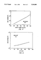
- FIGS. 4 and 5 illustrate non-melt dose as a function of laser energy and as a function of number of pulses, respectively.
- FIG. 6 and 7 illustrates SIMS results for a sample having a silicide film.
- FIGS. 8A-8C illustrate dose versus number of pulses, junction depth versus number of pulses, and interface versus number of pulses for samples with silicide films.
- FIG. 9 illustrates SIMS results for other samples doped in accordance with the invention.
- FIG. 1 is a schematic of gas immersion laser doping apparatus which employs the present invention.
- a gas cell 10 containing a semiconductor wafer immersed in a dopant gas is mounted on an XY table 12 with the wafer irradiated by a laser beam from a 308 nm XECL excimer laser 14 which passes through optics 18 thence through a window in the gas cell for irradiation of the wafer.
- the laser 14 and XY table 12 are controlled during processing by a computer 20.
- a CCD camera 22 and monitor 24 continuously view the wafer during processing.
- An HeNe laser 26 and oscilloscope 28 are used to monitor the non-melt condition as the wafer is doped.
- the gas cell can be stationary while the laser is moved along X and Y coordinates.
- the gas cell is filled with the desired dopant gas such as BF 3 , ASF 5 , or PF 5 .
- the gas pressure can be on the order of 50 Torr with the gas composition being up to 100% of the dopant gas.
- the dose of dopant depends on dopant gas concentration and pressure along with pulse intensity. Repetition rate can also affect the dose.
- the wafer is first cleaned between pre-dep and drive-in steps using standard organic, metal cleaning procedures and a 50:1 HF dip, for example.
- a concentrated vapor HF etch is used immediately prior to loading a wafer into the gas chamber.
- the wafer is suitably masked with a laser reflecting material or heat shield such as aluminum, polycrystalline silicon, oxides of silicon, and other metals so that only selected regions on the surface of the wafer are irradiated.
- the technique can be applied in forming shallow junctions by outdiffusion from silicide films as has been demonstrated on tungsten silicide films using BF 3 gas ambient as a source for boron doping and PF 5 gas ambient as a source for n-type phosphorus doping.
- gas pressure and composition were 50 Torr and 100% BF 3 , typical of those used in the standard GILD process.
- Laser energy fluences were 600 mi/cm -2 and 700 mJ/cm -2 .
- 1-500 pulses have been repeated at a 9 Hz rate. Using 600 mJ/cm -2 , approximately 1 e13 boron atoms cm -2 were incorporated in a first heating pulse.
- Interface concentration of 2 e20 boron atoms cm -3 was achieved using 100 pulses at 600 mj/cm -2 energy fluence. For these conditions, 100 pulses at 600 mJ/cm -2 , no melting of the silicide film was detected using an HeNe laser reflectivity probe.
- the method can be applied to other silicides such as cobalt silicide and to other dopants such as arsenic.
- a variation on the technique is to use the laser to incorporate a high concentration of dopant in the silicide layer only, and use outdiffusing techniques such as rapid thermal lamp annealing to drive the dopants into the silicon.
- the laser can also be used to outdiffuse dopants which were incorporated in the silicide by other means such as ion implantation.
- FIG. 2 presents SIMS results from a non-melt boron doped sample which shows a 600 ⁇ junction depth and a ⁇ 7.3e12 cm -2 dose fabricated using 500 non-melt pulses at 5 Hz repetition rate.
- FIG. 3 presents the SIMS results for a sample which received 20 non-melt pre-dep pulses and 15 drive-in pulses at 17.5 ns melt duration.
- Pre-dep was conducted in a 53.2 Torr PF 5 gaseous ambient, and drive-in was conducted in 50 Torr N 2 .
- the wafer was cleaned using a 30second HF vapor etch between predep and drive-in.
- the non-melt dose as a function of laser energy and as a function of number of pulses is shown in FIGS. 4 and 5, respectively. These figures show that good control over dose can be obtained by varying either the laser energy or by varying the number of pulses.
- n-source and -drain layers have been achieved and as required for a hot-carrier suppressed MOSFET, such as shown in Tasch, U.S. Pat. No. 5,012,306 for Hot-Carrier Suppressed SubMjcron MOSFET Device.
- the layers were fabricated using a non-melt pre-dep in a PF 5 gaseous ambient, followed by a melt drive-in (20-35 ns melt duration) in a nitrogen ambient.
- Doping of silicide films from the gas phase can be achieved using modifications to the standard GILD process similar to those made for non-melt doping, i.e., low laser energies and many pulses per die.
- a 2500 ⁇ thick WSi 2 film was deposited on an n-type wafer in a GENUS LPCVD system and subsequently annealed at 1000° C. for 30 minutes. Following a cleaning procedure (4:1 H 2 SO 4 :H 2 O 2 /rinse, 5:1:1 HCl:H 2 O 2 :H 2 O/rinse, spin dry) , the wafer was immersed in a 55 Torr BF 3 dopant gas ambient and then subjected to a matrix of laser conditions.
- Sample H6 received 100 pulses, at 9 Hz rep rate, and laser energy fluence 600 mJ/cm 2 .
- GILD doping of WSi 2 films and the underlying silicon substrate was monitored using SIMS.
- FIG. 6 gives the processed SIMS data for boron-doped sample.
- FIG. 7 shows processed SIMS data for a phosphorus doped sample which received 500 pulses at 1.2 j/cm 2 laser energy fluence.
- Results are presented in FIG. 9 for n-type doping of tungsten silicide films using PF 5 gaseous dopant source.
- the SIMS results show high interface concentration (>10 20 P/cm 3 ) and shallow junction ( ⁇ 1500 ⁇ ).
- the roughening of the film/substrate interface which is indicated by the broad W and P tails is believed to be due to the Cs+ion bombardment during SIMS and not due to the laser process, since these tails are observed in the cesium bombardment spectra of non-laser processed samples as well.
- the interface roughness of these non-laser processed samples is close to that of the non-laser processed samples, which were analyzed using oxygen ion bombardment, since the silicide films were deposited in the same run.
- the samples analyzed using oxygen ion bombardment did not exhibit broad tiling, ana RBS analysis and TEM micrographs did not indicate rough interfaces.
- Control over dose is achieved by varying the number of laser pulses. This is illustrated in FIG. 8A which plots boron dose versus number of laser pulses.
- FIGS. 8B and 8C plot junction depth versus number of pulses and interface concentration versus number of pulses, respectively.
Landscapes
- Engineering & Computer Science (AREA)
- Physics & Mathematics (AREA)
- Condensed Matter Physics & Semiconductors (AREA)
- General Physics & Mathematics (AREA)
- Manufacturing & Machinery (AREA)
- Computer Hardware Design (AREA)
- Microelectronics & Electronic Packaging (AREA)
- Power Engineering (AREA)
- Insulated Gate Type Field-Effect Transistor (AREA)
Abstract
Description
Claims (19)
Priority Applications (1)
| Application Number | Priority Date | Filing Date | Title |
|---|---|---|---|
| US07/993,788 US5316969A (en) | 1992-12-21 | 1992-12-21 | Method of shallow junction formation in semiconductor devices using gas immersion laser doping |
Applications Claiming Priority (1)
| Application Number | Priority Date | Filing Date | Title |
|---|---|---|---|
| US07/993,788 US5316969A (en) | 1992-12-21 | 1992-12-21 | Method of shallow junction formation in semiconductor devices using gas immersion laser doping |
Publications (1)
| Publication Number | Publication Date |
|---|---|
| US5316969A true US5316969A (en) | 1994-05-31 |
Family
ID=25539932
Family Applications (1)
| Application Number | Title | Priority Date | Filing Date |
|---|---|---|---|
| US07/993,788 Expired - Lifetime US5316969A (en) | 1992-12-21 | 1992-12-21 | Method of shallow junction formation in semiconductor devices using gas immersion laser doping |
Country Status (1)
| Country | Link |
|---|---|
| US (1) | US5316969A (en) |
Cited By (23)
| Publication number | Priority date | Publication date | Assignee | Title |
|---|---|---|---|---|
| US5424244A (en) * | 1992-03-26 | 1995-06-13 | Semiconductor Energy Laboratory Co., Ltd. | Process for laser processing and apparatus for use in the same |
| WO1996008839A1 (en) * | 1994-09-13 | 1996-03-21 | Siemens Aktiengesellschaft | Method of producing a doped region in a monocrystalline semiconductor substrate |
| EP0757598A1 (en) * | 1995-01-23 | 1997-02-12 | Sandia Corporation | Pulsed ion beam assisted deposition |
| WO1997027620A1 (en) * | 1996-01-29 | 1997-07-31 | The Regents Of The University Of California | A self-aligned lightly-doped-drain structure for mos transistors |
| EP0834190A2 (en) * | 1995-06-05 | 1998-04-08 | The Regents Of The University Of California | Method for shallow junction formation |
| US5795627A (en) * | 1997-02-14 | 1998-08-18 | Advanced Micro Devices, Inc. | Method for annealing damaged semiconductor regions allowing for enhanced oxide growth |
| US5810945A (en) * | 1993-05-12 | 1998-09-22 | Max-Planck-Gesellschaft Zur Forderung Der Wissenschaften E.V. | Method of fabricating an electronic micropatterned electrode device |
| US5885904A (en) * | 1997-02-14 | 1999-03-23 | Advanced Micro Devices, Inc. | Method to incorporate, and a device having, oxide enhancement dopants using gas immersion laser doping (GILD) for selectively growing an oxide layer |
| US5904575A (en) * | 1997-02-14 | 1999-05-18 | Advanced Micro Devices, Inc. | Method and apparatus incorporating nitrogen selectively for differential oxide growth |
| US5918140A (en) * | 1997-06-16 | 1999-06-29 | The Regents Of The University Of California | Deposition of dopant impurities and pulsed energy drive-in |
| US5998272A (en) * | 1996-11-12 | 1999-12-07 | Advanced Micro Devices, Inc. | Silicidation and deep source-drain formation prior to source-drain extension formation |
| US6040019A (en) * | 1997-02-14 | 2000-03-21 | Advanced Micro Devices, Inc. | Method of selectively annealing damaged doped regions |
| US6214684B1 (en) * | 1995-09-29 | 2001-04-10 | Canon Kabushiki Kaisha | Method of forming a semiconductor device using an excimer laser to selectively form the gate insulator |
| US6221726B1 (en) * | 1995-10-26 | 2001-04-24 | The Regents Of The University Of Claifornia | Process for fabricating device structures for real-time process control of silicon doping |
| US6284443B1 (en) | 1999-04-30 | 2001-09-04 | International Business Machines Corporation | Method and apparatus for image adjustment |
| US6300228B1 (en) | 1999-08-30 | 2001-10-09 | International Business Machines Corporation | Multiple precipitation doping process |
| US6344116B2 (en) | 1985-11-19 | 2002-02-05 | Raymond M. Warner, Jr. | Monocrystalline three-dimensional integrated-circuit technology |
| US6395624B1 (en) | 1999-02-22 | 2002-05-28 | International Business Machines Corporation | Method for forming implants in semiconductor fabrication |
| US6451644B1 (en) * | 1998-11-06 | 2002-09-17 | Advanced Micro Devices, Inc. | Method of providing a gate conductor with high dopant activation |
| US6720241B2 (en) * | 2001-06-18 | 2004-04-13 | Matsushita Electric Industrial Co., Ltd. | Method for manufacturing semiconductor device |
| DE102004036220A1 (en) * | 2004-07-26 | 2006-03-23 | Jürgen H. Werner | Laser doping of solids with a line-focused laser beam and based on this production of solar cell emitters |
| US20100323532A1 (en) * | 2006-03-08 | 2010-12-23 | Paul Carey | Method of thermal processing structures formed on a substrate |
| US20110185971A1 (en) * | 2009-11-30 | 2011-08-04 | Uvtech Systems, Inc. | Laser doping |
Citations (6)
| Publication number | Priority date | Publication date | Assignee | Title |
|---|---|---|---|---|
| US4151008A (en) * | 1974-11-15 | 1979-04-24 | Spire Corporation | Method involving pulsed light processing of semiconductor devices |
| US4558507A (en) * | 1982-11-12 | 1985-12-17 | Nec Corporation | Method of manufacturing semiconductor device |
| US4661177A (en) * | 1985-10-08 | 1987-04-28 | Varian Associates, Inc. | Method for doping semiconductor wafers by rapid thermal processing of solid planar diffusion sources |
| US4669176A (en) * | 1984-07-30 | 1987-06-02 | Seiko Epson Kabushiki Kaisha | Method for diffusing a semiconductor substrate through a metal silicide layer by rapid heating |
| US4914500A (en) * | 1987-12-04 | 1990-04-03 | At&T Bell Laboratories | Method for fabricating semiconductor devices which include sources and drains having metal-containing material regions, and the resulting devices |
| US5114876A (en) * | 1990-12-07 | 1992-05-19 | The United States Of America As Represented By The United States Department Of Energy | Selective epitaxy using the gild process |
-
1992
- 1992-12-21 US US07/993,788 patent/US5316969A/en not_active Expired - Lifetime
Patent Citations (6)
| Publication number | Priority date | Publication date | Assignee | Title |
|---|---|---|---|---|
| US4151008A (en) * | 1974-11-15 | 1979-04-24 | Spire Corporation | Method involving pulsed light processing of semiconductor devices |
| US4558507A (en) * | 1982-11-12 | 1985-12-17 | Nec Corporation | Method of manufacturing semiconductor device |
| US4669176A (en) * | 1984-07-30 | 1987-06-02 | Seiko Epson Kabushiki Kaisha | Method for diffusing a semiconductor substrate through a metal silicide layer by rapid heating |
| US4661177A (en) * | 1985-10-08 | 1987-04-28 | Varian Associates, Inc. | Method for doping semiconductor wafers by rapid thermal processing of solid planar diffusion sources |
| US4914500A (en) * | 1987-12-04 | 1990-04-03 | At&T Bell Laboratories | Method for fabricating semiconductor devices which include sources and drains having metal-containing material regions, and the resulting devices |
| US5114876A (en) * | 1990-12-07 | 1992-05-19 | The United States Of America As Represented By The United States Department Of Energy | Selective epitaxy using the gild process |
Cited By (37)
| Publication number | Priority date | Publication date | Assignee | Title |
|---|---|---|---|---|
| US6344116B2 (en) | 1985-11-19 | 2002-02-05 | Raymond M. Warner, Jr. | Monocrystalline three-dimensional integrated-circuit technology |
| US6358784B1 (en) | 1992-03-26 | 2002-03-19 | Semiconductor Energy Laboratory Co., Ltd. | Process for laser processing and apparatus for use in the same |
| US7169657B2 (en) | 1992-03-26 | 2007-01-30 | Semiconductor Energy Laboratory Co., Ltd. | Process for laser processing and apparatus for use in the same |
| US7781271B2 (en) | 1992-03-26 | 2010-08-24 | Semiconductor Energy Laboratory Co., Ltd. | Process for laser processing and apparatus for use in the same |
| US6655767B2 (en) | 1992-03-26 | 2003-12-02 | Semiconductor Energy Laboratory Co., Ltd. | Active matrix display device |
| US20070119815A1 (en) * | 1992-03-26 | 2007-05-31 | Semiconductor Energy Laboratory Co., Ltd. | Process for laser processing and apparatus for use in the same |
| US5849043A (en) * | 1992-03-26 | 1998-12-15 | Semiconductor Energy Laboratory Co., Ltd. | Apparatus for laser ion doping |
| US5424244A (en) * | 1992-03-26 | 1995-06-13 | Semiconductor Energy Laboratory Co., Ltd. | Process for laser processing and apparatus for use in the same |
| US20040115940A1 (en) * | 1992-03-26 | 2004-06-17 | Semiconductor Energy Laboratory Co., Ltd. | Process for laser processing and apparatus for use in the same |
| US5810945A (en) * | 1993-05-12 | 1998-09-22 | Max-Planck-Gesellschaft Zur Forderung Der Wissenschaften E.V. | Method of fabricating an electronic micropatterned electrode device |
| WO1996008839A1 (en) * | 1994-09-13 | 1996-03-21 | Siemens Aktiengesellschaft | Method of producing a doped region in a monocrystalline semiconductor substrate |
| EP0757598A4 (en) * | 1995-01-23 | 2001-03-14 | Sandia Corp | Pulsed ion beam assisted deposition |
| EP0757598A1 (en) * | 1995-01-23 | 1997-02-12 | Sandia Corporation | Pulsed ion beam assisted deposition |
| EP0834190A2 (en) * | 1995-06-05 | 1998-04-08 | The Regents Of The University Of California | Method for shallow junction formation |
| EP0834190A4 (en) * | 1995-06-05 | 1999-07-28 | Univ California | Method for shallow junction formation |
| US6214684B1 (en) * | 1995-09-29 | 2001-04-10 | Canon Kabushiki Kaisha | Method of forming a semiconductor device using an excimer laser to selectively form the gate insulator |
| US6221726B1 (en) * | 1995-10-26 | 2001-04-24 | The Regents Of The University Of Claifornia | Process for fabricating device structures for real-time process control of silicon doping |
| US6303446B1 (en) * | 1996-01-29 | 2001-10-16 | The Regents Of The University Of California | Method of making self-aligned lightly-doped-drain structure for MOS transistors |
| WO1997027620A1 (en) * | 1996-01-29 | 1997-07-31 | The Regents Of The University Of California | A self-aligned lightly-doped-drain structure for mos transistors |
| US5998272A (en) * | 1996-11-12 | 1999-12-07 | Advanced Micro Devices, Inc. | Silicidation and deep source-drain formation prior to source-drain extension formation |
| US5885904A (en) * | 1997-02-14 | 1999-03-23 | Advanced Micro Devices, Inc. | Method to incorporate, and a device having, oxide enhancement dopants using gas immersion laser doping (GILD) for selectively growing an oxide layer |
| US5904575A (en) * | 1997-02-14 | 1999-05-18 | Advanced Micro Devices, Inc. | Method and apparatus incorporating nitrogen selectively for differential oxide growth |
| US5795627A (en) * | 1997-02-14 | 1998-08-18 | Advanced Micro Devices, Inc. | Method for annealing damaged semiconductor regions allowing for enhanced oxide growth |
| US6040019A (en) * | 1997-02-14 | 2000-03-21 | Advanced Micro Devices, Inc. | Method of selectively annealing damaged doped regions |
| US5918140A (en) * | 1997-06-16 | 1999-06-29 | The Regents Of The University Of California | Deposition of dopant impurities and pulsed energy drive-in |
| USRE39988E1 (en) * | 1997-06-16 | 2008-01-01 | The Regents Of The University Of California | Deposition of dopant impurities and pulsed energy drive-in |
| US6451644B1 (en) * | 1998-11-06 | 2002-09-17 | Advanced Micro Devices, Inc. | Method of providing a gate conductor with high dopant activation |
| US6395624B1 (en) | 1999-02-22 | 2002-05-28 | International Business Machines Corporation | Method for forming implants in semiconductor fabrication |
| US6284443B1 (en) | 1999-04-30 | 2001-09-04 | International Business Machines Corporation | Method and apparatus for image adjustment |
| US6300228B1 (en) | 1999-08-30 | 2001-10-09 | International Business Machines Corporation | Multiple precipitation doping process |
| US6720241B2 (en) * | 2001-06-18 | 2004-04-13 | Matsushita Electric Industrial Co., Ltd. | Method for manufacturing semiconductor device |
| DE102004036220A1 (en) * | 2004-07-26 | 2006-03-23 | Jürgen H. Werner | Laser doping of solids with a line-focused laser beam and based on this production of solar cell emitters |
| US20080026550A1 (en) * | 2004-07-26 | 2008-01-31 | Werner Jurgen H | Laser doping of solid bodies using a linear-focussed laser beam and production of solar-cell emitters based on said method |
| DE102004036220B4 (en) * | 2004-07-26 | 2009-04-02 | Jürgen H. Werner | Method for laser doping of solids with a line-focused laser beam |
| US20100323532A1 (en) * | 2006-03-08 | 2010-12-23 | Paul Carey | Method of thermal processing structures formed on a substrate |
| US10141191B2 (en) * | 2006-03-08 | 2018-11-27 | Applied Materials, Inc. | Method of thermal processing structures formed on a substrate |
| US20110185971A1 (en) * | 2009-11-30 | 2011-08-04 | Uvtech Systems, Inc. | Laser doping |
Similar Documents
| Publication | Publication Date | Title |
|---|---|---|
| US5316969A (en) | Method of shallow junction formation in semiconductor devices using gas immersion laser doping | |
| Carey et al. | Ultra-shallow high-concentration boron profiles for CMOS processing | |
| EP1012879B1 (en) | Fabrication method for reduced-dimension integrated circuits | |
| KR100839259B1 (en) | Method of forming ultrashallow junctions by laser annealing and rapid thermal annealing | |
| US4151008A (en) | Method involving pulsed light processing of semiconductor devices | |
| US5474940A (en) | Method of fabricating a semiconductor device having shallow junctions in source-drain regions and a gate electrode with a low resistance silicide layer | |
| US5236865A (en) | Method for simultaneously forming silicide and effecting dopant activation on a semiconductor wafer | |
| US6051483A (en) | Formation of ultra-shallow semiconductor junction using microwave annealing | |
| JP4166298B2 (en) | Method of introducing chemical elements into receiving materials | |
| US6348367B1 (en) | Method for manufacturing a semiconductor device | |
| EP0069327A2 (en) | Method of laser annealing a subsurface region in a semiconductor | |
| US4925812A (en) | Platinum diffusion process | |
| US6130144A (en) | Method for making very shallow junctions in silicon devices | |
| EP0231794A2 (en) | Method and apparatus for forming metal silicide/silicon structures | |
| US6383902B1 (en) | Method for producing a microelectronic semiconductor component | |
| Gibbons | Applications of scanning cw lasers and electron beams in silicon technology | |
| Wong et al. | Excimer-laser doping of spin-on dopant in silicon | |
| Pai et al. | Rapid thermal annealing of Al‐Si contacts | |
| Murto et al. | Activation and deactivation studies of laser thermal annealed boron, arsenic, phosphorus, and antimony ultra-shallow abrupt junctions | |
| US6204160B1 (en) | Method for making electrical contacts and junctions in silicon carbide | |
| Kiang et al. | Modification of semiconductor device characteristics by lasers | |
| Panknin et al. | Dose Dependence of the Flash Lamp Annealing of Arsenic‐Implanted Silicon | |
| Chong et al. | Reduction of carrier depletion in p/sup+/polysilicon gates using laser thermal processing | |
| Benyaich et al. | Realignment of As doped polycrystalline Si films by double step annealing | |
| Laviron et al. | Excimer-laser activation of dopants in silicon: a new concept for a uniform treatment over a whole die area |
Legal Events
| Date | Code | Title | Description |
|---|---|---|---|
| AS | Assignment |
Owner name: BOARD OF TRUSTEES OF THE LELAND STANFORD JUNIOR UN Free format text: ASSIGNMENT OF ASSIGNORS INTEREST;ASSIGNORS:ISHIDA, EMI;SIGMON, THOMAS W.;LYNCH, WILLIAM T.;REEL/FRAME:006903/0772 Effective date: 19940307 |
|
| AS | Assignment |
Owner name: BOARD OF TRUSTEES OF THE LELAND STANFORD JUNIOR UN Free format text: ASSIGNMENT OF ASSIGNORS INTEREST;ASSIGNORS:ISHIDA, EMI;SIGMON, THOMAS W.;LYNCH, WILLIAM T.;REEL/FRAME:006920/0059 Effective date: 19940307 |
|
| AS | Assignment |
Owner name: BOARD OF TRUSTEES OF THE LELAND STANFORD JUNIOR UN Free format text: ASSIGNMENT OF ASSIGNORS INTEREST;ASSIGNORS:ISHIDA, EMI;SIGMON, THOMAS W.;LYNCH, WILLIAM T.;REEL/FRAME:006937/0235 Effective date: 19940329 |
|
| STCF | Information on status: patent grant |
Free format text: PATENTED CASE |
|
| FPAY | Fee payment |
Year of fee payment: 4 |
|
| FPAY | Fee payment |
Year of fee payment: 8 |
|
| FPAY | Fee payment |
Year of fee payment: 12 |