EP0304591A2 - Mémoire à semi-conducteurs avec détecteur de changement de signal - Google Patents
Mémoire à semi-conducteurs avec détecteur de changement de signal Download PDFInfo
- Publication number
- EP0304591A2 EP0304591A2 EP88110880A EP88110880A EP0304591A2 EP 0304591 A2 EP0304591 A2 EP 0304591A2 EP 88110880 A EP88110880 A EP 88110880A EP 88110880 A EP88110880 A EP 88110880A EP 0304591 A2 EP0304591 A2 EP 0304591A2
- Authority
- EP
- European Patent Office
- Prior art keywords
- circuit
- gate
- field effect
- output
- semiconductor memory
- Prior art date
- Legal status (The legal status is an assumption and is not a legal conclusion. Google has not performed a legal analysis and makes no representation as to the accuracy of the status listed.)
- Granted
Links
- 230000008859 change Effects 0.000 title claims abstract description 25
- 239000004065 semiconductor Substances 0.000 title claims abstract description 22
- 230000003213 activating effect Effects 0.000 claims abstract description 5
- 230000015654 memory Effects 0.000 claims description 44
- 230000005669 field effect Effects 0.000 claims description 29
- 238000001514 detection method Methods 0.000 claims description 11
- 101100136063 Mycobacterium tuberculosis (strain ATCC 25618 / H37Rv) PE11 gene Proteins 0.000 claims description 5
- 101100136064 Mycobacterium tuberculosis (strain ATCC 25618 / H37Rv) PE13 gene Proteins 0.000 claims description 3
- 101150087801 PE23 gene Proteins 0.000 claims description 3
- 238000011144 upstream manufacturing Methods 0.000 claims description 3
- 238000010586 diagram Methods 0.000 description 4
- 238000000034 method Methods 0.000 description 4
- 230000008569 process Effects 0.000 description 4
- 230000008901 benefit Effects 0.000 description 2
- 230000000903 blocking effect Effects 0.000 description 2
- 239000003795 chemical substances by application Substances 0.000 description 2
- 230000000295 complement effect Effects 0.000 description 2
- 238000005516 engineering process Methods 0.000 description 2
- 230000004913 activation Effects 0.000 description 1
- 238000010276 construction Methods 0.000 description 1
- 238000006880 cross-coupling reaction Methods 0.000 description 1
- 230000009849 deactivation Effects 0.000 description 1
- 230000001934 delay Effects 0.000 description 1
- 230000003111 delayed effect Effects 0.000 description 1
- 238000011161 development Methods 0.000 description 1
- 230000018109 developmental process Effects 0.000 description 1
- 238000004519 manufacturing process Methods 0.000 description 1
- 230000007420 reactivation Effects 0.000 description 1
- 230000009467 reduction Effects 0.000 description 1
- 230000004044 response Effects 0.000 description 1
- 230000000630 rising effect Effects 0.000 description 1
- 230000003068 static effect Effects 0.000 description 1
- 230000007704 transition Effects 0.000 description 1
Images

Classifications
-
- G—PHYSICS
- G11—INFORMATION STORAGE
- G11C—STATIC STORES
- G11C7/00—Arrangements for writing information into, or reading information out from, a digital store
-
- G—PHYSICS
- G11—INFORMATION STORAGE
- G11C—STATIC STORES
- G11C7/00—Arrangements for writing information into, or reading information out from, a digital store
- G11C7/22—Read-write [R-W] timing or clocking circuits; Read-write [R-W] control signal generators or management
-
- G—PHYSICS
- G11—INFORMATION STORAGE
- G11C—STATIC STORES
- G11C11/00—Digital stores characterised by the use of particular electric or magnetic storage elements; Storage elements therefor
- G11C11/21—Digital stores characterised by the use of particular electric or magnetic storage elements; Storage elements therefor using electric elements
- G11C11/34—Digital stores characterised by the use of particular electric or magnetic storage elements; Storage elements therefor using electric elements using semiconductor devices
- G11C11/40—Digital stores characterised by the use of particular electric or magnetic storage elements; Storage elements therefor using electric elements using semiconductor devices using transistors
- G11C11/41—Digital stores characterised by the use of particular electric or magnetic storage elements; Storage elements therefor using electric elements using semiconductor devices using transistors forming static cells with positive feedback, i.e. cells not needing refreshing or charge regeneration, e.g. bistable multivibrator or Schmitt trigger
- G11C11/413—Auxiliary circuits, e.g. for addressing, decoding, driving, writing, sensing, timing or power reduction
- G11C11/417—Auxiliary circuits, e.g. for addressing, decoding, driving, writing, sensing, timing or power reduction for memory cells of the field-effect type
- G11C11/419—Read-write [R-W] circuits
-
- G—PHYSICS
- G11—INFORMATION STORAGE
- G11C—STATIC STORES
- G11C7/00—Arrangements for writing information into, or reading information out from, a digital store
- G11C7/12—Bit line control circuits, e.g. drivers, boosters, pull-up circuits, pull-down circuits, precharging circuits, equalising circuits, for bit lines
Definitions
- the invention relates to a semiconductor memory with a signal change detection circuit according to the preamble of claim 1.
- a semiconductor memory of this type is known from EP-A-0 107 415.
- an output signal is derived in the signal change detection circuit from each address signal change, which is first fed to a first control input of the precharge circuit, at which it causes the same to be deactivated.
- the output signal is fed via a delay unit to a second control input of the precharge circuit, at which it causes the same to be reactivated.
- the delay unit delays the output signal by a fixed period of time, which must be provided for the most time-consuming memory access.
- the invention has for its object to provide a semiconductor memory of the type mentioned, in which a timing of the precharge circuit derived from signal changes can be matched to the actual duration of the individual memory accesses much better than is the case with the known semiconductor memory mentioned above. This is achieved according to the invention by training according to the characterizing part of patent claim 1.
- the advantage that can be achieved with the invention is, in particular, that the precharge circuit can be reactivated as soon as possible after the end of each individual memory access, so that the memory is available for a new access in the shortest possible time.
- Another advantage is that the extremely fast reactivation of the front charging circuit is also guaranteed regardless of the number of memory cells in the memory field and thus regardless of the resulting different duration of memory access.
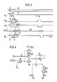
- FIG. 1 denotes a memory field which is constructed from a multiplicity of static memory cells, for example according to FIG. 2, in complementary circuit technology.
- each of these memory cells has two cross-coupled inverters, the first of which consists of the series connection of two field effect transistors T1 and T2, the second of the series connection of two field effect transistors T3 and T4.
- the source connections of the p-channel transistors T1 and T3 are connected to a connection 2 which is connected to a supply voltage V DD of, for example, 5 V.
- the source connections the n-channel transistors T2 and T4 are connected to a terminal 3 which is connected to the reference potential V SS .
- the drain connections of T1 and T2 are connected to one another in a node 4, the drain connections of the transistors T3 and T4 in a node 5.
- the interconnected gate connections of T1 and T2 are connected to the node 5 and the interconnected gate connections of T3 and T4 with node 4.
- Nodes 4 and 5 are each connected to data lines L and via the source-drain paths of n-channel selection transistors T5 and T6 L connected.
- the gates of T5 and T6 are controlled via a word line WL.
- the memory cells are combined in rows and columns in the memory array 1, in such a way that all the memory cells of a row are located on a common word line WL, while all of the memory cells of a column have a common data line pair L, L exhibit.
- the word lines of all lines of the memory array 1 are designated WL i in FIG. 1, the data line pairs L, L all columns with L i , L i .
- the data line pairs L i , L i are connected on the one hand to the inputs of a sense amplifier 6 and on the other hand to the outputs of a write-in circuit 7. Furthermore, they are connected to the outputs 8 of a precharge circuit 9, through which they can be supplied with a predetermined potential.
- the precharge circuit 9 contains, for example, n-channel transistors, the source connections of which represent the outputs 8, their drain connections being connected to the supply voltage V DD .
- the control connections of the n-channel transistors are connected to a control input 10.
- the outputs 11a, 11b of the sense amplifier 6 are connected to a data output DA via a buffer 12 and a buffer amplifier 13, while a data input DE is connected to an input 15 of the write-in circuit 7 via a buffer amplifier 14.
- a block 16 represents the row decoding, a block 17 the column decoding and the write / read control of the semiconductor memory.
- n-digit that is to say n-bit, address signal A
- n-bit that is to say n-bit, address signal A
- n inputs 16a of the row decoding 16 over n lines 18 and n buffer amplifier 19 connected to n inputs 20, and n inputs 17a of 17 via n lines 21 and the buffer amplifier 19 also to the inputs 20.
- the outputs of the row decoding 16 are connected to the word lines WL i , the outputs of the column decoding and writing / Read controller 17 via output lines 22 and 23 to the circuit units 6, 7, 12, 13 and 14.
- a further line 21 connects a further input 20, to which a read / write signal RW is present, to a further input 17a of FIG Finally, an input 20 is also provided, to which a chip select signal CS is fed and which is connected to additional inputs 16a and 17a via additional lines 18 and 21.
- a total of n + 2 inputs 20 are therefore provided, which are connected to the inputs of n + 2 identically constructed signal change detection circuits 24, the common output 25 of which is connected to a first input of a clock voltage generator 26.
- a second input 27 of the clock voltage generator 26 is connected to the output 28a of a control circuit 28, the inputs of which are at the outputs 11a and 11b of the sense amplifier 6.
- a first output 29 of 26 is connected to the control input 10 of the precharge circuit 9, while a second output 30 of 26 is connected via a line 31 to an input of the column decoding and read / write control 17 and additionally via a line 32 to an input 16b of the row decoding 16 can be connected.
- the output line 22 of FIG. 17 is also connected to a further input of the control circuit 28.
- the inputs 20 are supplied with a corresponding address signal A which differs from the previously applied address signal, so that an address signal change takes place.
- This is represented in FIG. 3 by the intersection 33 of two voltage profiles plotted over time t.
- the one voltage curve U1 can represent a bit of a first address signal which, at time t1, changes from an upper voltage value, for example a "1", to a lower voltage value, eg a "0" changes while the other voltage curve U2 illustrates a bit of a second address signal which changes from "0" to "1" at time t1.
- At least one of the signal change detection circuits 24 derives a pulse-shaped output signal 34 from the address signal change at time t1, the falling edge of which (transition from “1 to” 0 ") is delayed by a time period D1 compared to t1.
- the clock voltage generator specifies at its output 29 from the time t1 a first clock voltage ⁇ VL , which is fed to the control input 10 of the precharge circuit, ⁇ VL has a voltage level "1" which activates the precharge circuit 9, so that the data lines L i , L i are preloaded to a predetermined potential.
- the falling edge of the output signal 34 causes, after a delay time of D2, the first clock voltage ⁇ VL to be switched to a voltage level "0" and thus a deactivation of the precharge circuit 9, that is to say the disconnection of the data lines from a voltage source causing the precharge.
- a second clock voltage ⁇ DK which occurs at the output 30, is switched from a voltage level "0" to a voltage level "1", which activates the column decoding and read / write circuit 17 and, if an internal clocking of the row decoding is provided leads to an activation of 16.
- the desired memory cell is thus addressed and the memory can be accessed.
- the sense amplifier 6 and the circuit units 12 and 13 are activated, which is done by means of the read / write signal R / W, which is switched to a first voltage level, while the write circuit 7 and the buffer amplifier 14 remain deactivated.
- the row decoding 16 then does not need to be activated or deactivated by means of the clock voltage ⁇ DK if the individual memory cells are dimensioned such that the data lines connected to the voltage source used for precharging together with a selected word line do not falsify the stored signals in the can lead to memory cells located on the selected word line.
- the control circuit 28 evaluates the read signal LA occurring at the outputs 11a and 11b of the sense amplifier 6, LA out. It recognizes whether a certain signal amplitude is exceeded. If this is the case, the output signal ⁇ R of the control circuit 28 goes from “1" to "0". 3, this occurs at time t2.
- the clock voltage generator 26 is controlled via its input 27 such that the clock voltage ⁇ DK is first switched from “1" to "0” after a delay time D3 and the clock voltage ⁇ VL after a delay time D4 exceeding D3 is switched back from "0" to "1".
- the output signal LA, LA reaches the buffer 12 via the outputs 11a, 11b and is transferred via the output and the buffer amplifier 13 to the data output DA. To the It is then available until a new signal occurs at the outputs 11a, 11b, which in turn is transferred to the buffer memory 12.
- the supply of the address signal assigned to this memory cell causes an address signal change which again results in an output signal 34 and at a time interval from D2 from its falling edge for deactivating the precharge circuit by means of ⁇ VL and for activating the Blocks 16 and 17 by means of ⁇ DK leads.
- This memory cell is thus addressed.
- the signal R / W is switched to a second voltage level, which characterizes a write-in process, so that an output signal 34 of the circuit 24 is generated even when the address signals A are not changed.
- Blocks 6, 7 and 14 are activated by the second voltage level of R / W, while 12 and 13 remain deactivated.
- the signal to be written now arrives via 14, 15 and 7 on the selected data line pair L, L and to the inputs of the sense amplifier 6, which leads to the output of an output signal LA, LA leads to the outputs 11a and 11b.
- the control circuit 28 evaluates this output signal again in that ⁇ R goes from “1” to “0".
- the falling edge 60 controls the clock voltage generator 26 such that ⁇ DK is switched back from “1” to “0” and ⁇ VL from "0" to "1".
- ⁇ R is switched from "0" to "1"
- the clock voltage generator 26 can again recognize a new signal 34 'of the circuit 24.
- the output signal 34 of the signal change detection circuit is here fed to the gate of a p-channel transistor P1, the source of which is connected to the supply voltage V DD via a connection 35 and the drain of which is connected to an internal node K1.
- the output signal ⁇ R of the control circuit 28 is applied to a first input of a NAND gate 36, the output of which is connected to the gate of an n-channel transistor N1.
- the source and drain of N1 are connected to the reference potential V SS and to the internal node K1.
- a second entrance 37 of gate 36 is expediently assigned a signal CS, which is referred to as a "chip select" signal.
- a holding circuit consisting of inverters I1 and I2 is connected to node K1.
- K1 is connected via a buffer amplifier 38 to the output 30, at which the clock voltage ⁇ DK is available.
- K1 is connected directly to the first input of a NOR gate 39 and via a delay circuit 40, for example an inverter chain, to a second input of 39.
- the output of 39 is led via a buffer amplifier 41 to the output 29, at which the clock voltage ⁇ VL is tapped.
- the circuit parts 39 and 40 provide a delay of the rising edge 42 of ⁇ VL compared to the falling edge 43 of ⁇ DK , which is necessary to ensure that the decoding of the memory is switched off before the precharge circuit 9 is switched on.
- the state of the node K1 can be set to "0" or "1” via the transistors N1 and P1.
- the falling edge of output signal 34 sets node K1 to "1” by switching P1 on. This state is then no longer changed by further output signals 34.
- ⁇ VL is set to "0” and ⁇ DK to "1”
- N1 has a substantially smaller resistance between its source and its drain connection than the transistor P1 in the conductive state.
- N1 and P1 must be dimensioned so that they deliver significantly more current than the inverter I2.
- connection 35 is expediently connected via a p-channel transistor P2 to a connection 35 'which is connected to the supply voltage V DD instead of 35.
- the gate of P2 is then connected to the output of NAND gate 36.
- P2 serves as a switching transistor which switches off the supply voltage V DD from the terminal 35 when the transistor N1 is switched on. This prevents the occurrence of a cross flow.
- Fig. 5 shows a preferred embodiment of the control circuit 28 and an appropriate circuit design of the sense amplifier 6.
- the sense amplifier 6 has 2n data line inputs, of which the first two designated E1 and E1 'and with the data lines L1 and L 1 the first column of the memory field 1 are connected.
- the drain of N21 is connected to the output 11a, the drain of N11 to the output 11b.
- the gate of N11 is connected to the input E1, the gate of N21 with the input E1 '.
- the node 42a is connected to the drain connection of the base transistor N31, the source of which is connected to reference potential via a connection 43a.
- the gate of N3 1 is connected via a connection 44 to a first output of the column decoding 17, to which a "1" is present when the data line pair L 1, L 1 is selected.
- the further data line inputs of the sense amplifier 6 are assigned in an analog manner to n-channel transistors which are connected in a corresponding manner to 11a and 11b, the gate connections of the base transistors being in each case at the other outputs of the column decoding 17.
- the inputs E n and E n 'assigned n-channel transistors are designated N1 n , N2 n and N3 n .
- the gate connection of the base transistor N3 n has the reference numeral 45, while 46 denotes the source terminal of N3 n , which is at reference potential.
- the output 11b is connected to the drain connection of a p-channel transistor PL1, the source connection of which lies at a node 47.
- the output 11a is connected to the drain connection of a p-channel transistor PL2, the source connection of which is connected to the node 47.
- the gate connection of PL1 is connected to the drain connection of PL2, the gate connection PL2 is connected to the drain connection of PL1.
- the node 47 is led via the source-drain path of a further p-channel transistor PS1 to a connection 48 which is connected to the supply voltage V DD .
- the outputs 11a and 11b are connected to one another via the source-drain path of an n-channel field-effect transistor N2, the gates of PS1 and N2 being connected to a connection 49.
- the transistors PL1 and PL2 represent a p-channel load part 50 of the sense amplifier 6.
- a buffer 12 and a buffer amplifier 13 are connected to the outputs 11a and 11b, the output of which represents the data output DA.
- the embodiment of the control circuit 28 shown in FIG. 5 contains three n-channel transistors NE1, NE2 and NE3, the first two of which are connected with their source connections to a node 51, the drain connection of NE1 at a node 52 and the drain connection of NE2 lie at a node 53.
- the gate of NE1 is connected to output 11a, the gate of NE2 is connected to output 11b.
- the node 51 is connected via the source-drain path of NE3 to a connection 54 which is at reference potential V SS .
- the gate connection of NE3 is designated 55.
- the node 52 is connected via the source-drain path of a p-channel transistor PE1 to a terminal 56 which is connected to the supply voltage V DD .
- the node 53 is connected via the source-drain path of a p-channel transistor PE2 to a connection 57, to which the supply voltage is likewise fed.
- the gate of PE1 is connected to the drain connection of PE2 and the gate of PE2 is connected to the drain connection of PE1.
- the nodes 52 and 53 are connected via the source Drain section of a p-channel transistor PE3 connected to one another, the gate of which is connected to terminal 55. Furthermore, the nodes 52 and 53 are led via inverters I3 and I4 to the inputs of a NOR gate 58, the output of which is connected to the output 28a via a buffer amplifier 59.
- the base transistor that belongs to the selected column is turned on.
- the signal present at connection 49 is switched from “1" to "0".
- the outputs 11a and 11b are decoupled from one another, the supply voltage V DD being applied to the node 47 through the switching on of PS1.
- the signal present at the gate terminal 55 which is inverted to the signal present at 49, is switched from "0" to "1”.
- the transistor NE3 is thus turned on, while the transistor PE3 blocks. Since the potentials on the selected data lines change in opposite directions depending on the signal to be read out, this is also the case at the outputs 11a and 11b of the sense amplifier 6 which represents a differential amplifier. The opposing potential changes occurring there are shown in FIG.
- LA and LA designated.
- LA or LA changes in the direction of the reference potential and a corresponding potential change also occurs at node 52 or 53, the This means that the response threshold of one of the inverters I3 or I4 is not reached.
- the relevant inverter thus recognizes an input signal “0” and applies a "1" to the downstream input of the NOR gate 58.
- the signal ⁇ R occurring at the output 28a is switched from “1” to "0".
- This changeover which is indicated in FIG. 3 by the falling edge 60 of ⁇ R , causes the transistor N1 to be turned on after the delay time D3 has elapsed, so that the node K1 (FIG.
- This switchover process sets the NAND gate 36 to an output signal "0", which leads to the blocking of N1, but the node K1 remains at "0" as long as P1 is also blocked.
- the clock voltage generator 26 is again sensitized to the next output signal 34, since the leading edge of P1 thereof is switched off by the falling edge thereof, whereby K1 is set to "1".
- the switching transistor PS1 is omitted in a sense amplifier 6, which is otherwise constructed according to FIG. 5, the circuit parts NE1 to NE3, PE1 to PE3, 52, 53, 56 and 57 of the control circuit 28 can also be omitted. In this case, the input of I3 is connected directly to output 11a, the input of I4 directly to 11b.
- the load part 50 of the sense amplifier 6 can also be designed such that the gates of PL1 and PL2 are connected to one another and connected to the drain connection of PL1.
- the gates of PL1 and PL2 can also be connected to one another and led to a reference voltage connection. In this case, however, the ab Simplification of the control circuit 28 described above is not permitted.
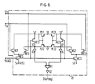
- FIG. 6 shows a further embodiment of the control circuit 28, in which a bistable circuit design, as is given by the cross-coupled transistors PE1 and PE2 in FIG. 5, is avoided.
- a first differential amplifier circuit which largely corresponds in structure to that shown in FIG. 5, is shown in the left part of FIG. 6.
- the n-channel transistors NE11 to NE13 and the p-channel transistors PE11 to PE13 correspond to the circuit parts NE1 to NE3 and PE1 to PE3 in FIG. 5, the difference being that the gate connections of PE11 and PE12 correspond to the Drain connection of PE11 are connected.
- node 53 is connected to an inverter input, but node 52 is no longer tapped via an inverter input.
- a second differential amplifier circuit which corresponds completely to the first in construction, forms the right part of the circuit according to FIG. 6. It contains n-channel transistors NE21 to NE23 and p-channel transistors PE21 to PE23 in a part on the left part of FIG. 6 corresponding circuit configuration.
- the gate connection of NE21 is connected to the output 11a, the gate connection of NE22 to the output 11b.
- the source connection of NE23 lying at reference potential V SS is designated 54 '.
- the drain connections of PE21 and PE22 are labeled 52 'and 53'. Again, only node 53 'is connected to an inverter input, node 52' is not.
- inverters I5 and I6 which correspond to inverters I3 and I4 of FIG. 5, are connected to nodes 53 and 53 'according to FIG. 6.
- the outputs of I5 and I6 are at the inputs of a NOR gate 61, the output of which is connected to the output 28a via a buffer amplifier 62.
- the nodes 52 and 53 and 52 'and 53' are precharged to a potential V DD -V t , where V t again means the threshold voltage of the transistors PE11 or PE12 or PE21 or PE22.
- V t again means the threshold voltage of the transistors PE11 or PE12 or PE21 or PE22.
- disturbances or production-related asymmetries between the transistors NE1 and NE2 or PE1 and PE2 can lead to the circuit adopting one of its two stable states without a signal swing occurring at the circuit points 11a and 11b.
- this danger only exists if the transistor PE3 is blocked for a long time before a signal swing occurs at 11a and 11b. 6, this danger is completely eliminated.
- a signal change detection circuit 24 is, for example, from IEEE journals. of Solid-State Circuits, Vol. SC-19, Oct. 1984, pp. 545-551.
- an output signal 34 circuits 24 constructed simultaneously connect each of the n + 2 inputs 20.
- the inputs E i , E i ' can also be connected to the outputs of an upstream amplifier stage instead of the data lines L i , ⁇ L i , which in turn are connected to the data lines mentioned is connected.
- the sense amplifier 6 shown in Fig. 5 can be simplified insofar as only one n-channel transistor circuit, for example that provided with the transistors N11 to N31, provided that the selection of the desired data line pair before the input, for example E1 and E1 ', The remaining single-stage sense amplifier is made, for example, in the upstream amplifier stages.
- the switching thresholds of the inverters I3 to I6 can be set in a manner known per se by the ratio of the channel widths of the p- and n-channel transistors contained in them to a relatively low value of, for example, 1.5 V when the supply voltage V DD is approximately Is 5 V. This ensures that the precharge potential at nodes 52, 53 and 53 ', which is lower than V DD by the threshold voltage V t, is still reliably recognized by the inverters as an input signal "1".
- a gate circuit 19a can be provided, which is controlled by means of ⁇ DK in such a way that it blocks during a memory access. This prevents further address signals from reaching decoders 16 and 17 during memory access.
- the word width of the memory is greater than 1 bit.
- m memory fields 1, precharge circuits 9, sense amplifiers 6, write circuits 7, intermediate memories 12, buffer amplifiers 13, 14 and data outputs and inputs DA, DE are provided.
- the outputs of blocks 16 and 17 are then each with m corresponding word and data lines or sense amplifiers, write circuits, intermediate memories and Buffer amplifiers connected.
- the control circuit 28 is expediently only connected to the outputs 11a and 11b of one of the m sense amplifiers.
Landscapes
- Engineering & Computer Science (AREA)
- Microelectronics & Electronic Packaging (AREA)
- Computer Hardware Design (AREA)
- Static Random-Access Memory (AREA)
- Read Only Memory (AREA)
- Oscillators With Electromechanical Resonators (AREA)
Priority Applications (1)
| Application Number | Priority Date | Filing Date | Title |
|---|---|---|---|
| AT88110880T ATE86407T1 (de) | 1987-08-18 | 1988-07-07 | Halbleiterspeicher mit einer signalwechselerkennungsschaltung. |
Applications Claiming Priority (2)
| Application Number | Priority Date | Filing Date | Title |
|---|---|---|---|
| DE3727548 | 1987-08-18 | ||
| DE3727548 | 1987-08-18 |
Publications (3)
| Publication Number | Publication Date |
|---|---|
| EP0304591A2 true EP0304591A2 (fr) | 1989-03-01 |
| EP0304591A3 EP0304591A3 (en) | 1990-08-16 |
| EP0304591B1 EP0304591B1 (fr) | 1993-03-03 |
Family
ID=6334001
Family Applications (1)
| Application Number | Title | Priority Date | Filing Date |
|---|---|---|---|
| EP88110880A Expired - Lifetime EP0304591B1 (fr) | 1987-08-18 | 1988-07-07 | Mémoire à semi-conducteurs avec détecteur de changement de signal |
Country Status (7)
| Country | Link |
|---|---|
| US (1) | US4924443A (fr) |
| EP (1) | EP0304591B1 (fr) |
| JP (1) | JP2641132B2 (fr) |
| KR (1) | KR960016424B1 (fr) |
| AT (1) | ATE86407T1 (fr) |
| DE (1) | DE3878784D1 (fr) |
| HK (1) | HK68894A (fr) |
Families Citing this family (4)
| Publication number | Priority date | Publication date | Assignee | Title |
|---|---|---|---|---|
| JP2667946B2 (ja) * | 1992-09-21 | 1997-10-27 | 三菱電機株式会社 | 半導体記憶装置 |
| US5615169A (en) * | 1995-08-31 | 1997-03-25 | Monolithic System Technology, Inc. | Method and structure for controlling internal operations of a DRAM array |
| US5708624A (en) * | 1996-11-27 | 1998-01-13 | Monolithic System Technology, Inc. | Method and structure for controlling internal operations of a DRAM array |
| JP4321988B2 (ja) * | 2002-03-27 | 2009-08-26 | 富士通マイクロエレクトロニクス株式会社 | 半導体記憶装置およびその制御方法 |
Family Cites Families (4)
| Publication number | Priority date | Publication date | Assignee | Title |
|---|---|---|---|---|
| US4355377A (en) * | 1980-06-30 | 1982-10-19 | Inmos Corporation | Asynchronously equillibrated and pre-charged static ram |
| JPS5963091A (ja) * | 1982-09-30 | 1984-04-10 | Fujitsu Ltd | スタテイツクメモリ回路 |
| US4558435A (en) * | 1983-05-31 | 1985-12-10 | Rca Corporation | Memory system |
| JPS6061985A (ja) * | 1983-09-14 | 1985-04-09 | Mitsubishi Electric Corp | 半導体記憶装置 |
-
1988
- 1988-07-07 DE DE8888110880T patent/DE3878784D1/de not_active Expired - Lifetime
- 1988-07-07 EP EP88110880A patent/EP0304591B1/fr not_active Expired - Lifetime
- 1988-07-07 AT AT88110880T patent/ATE86407T1/de not_active IP Right Cessation
- 1988-07-15 US US07/219,271 patent/US4924443A/en not_active Expired - Lifetime
- 1988-08-15 JP JP63203687A patent/JP2641132B2/ja not_active Expired - Fee Related
- 1988-08-18 KR KR1019880010499A patent/KR960016424B1/ko not_active Expired - Fee Related
-
1994
- 1994-07-14 HK HK68894A patent/HK68894A/xx not_active IP Right Cessation
Also Published As
| Publication number | Publication date |
|---|---|
| JP2641132B2 (ja) | 1997-08-13 |
| HK68894A (en) | 1994-07-22 |
| EP0304591A3 (en) | 1990-08-16 |
| JPS6466896A (en) | 1989-03-13 |
| KR890004322A (ko) | 1989-04-21 |
| US4924443A (en) | 1990-05-08 |
| ATE86407T1 (de) | 1993-03-15 |
| DE3878784D1 (de) | 1993-04-08 |
| KR960016424B1 (ko) | 1996-12-11 |
| EP0304591B1 (fr) | 1993-03-03 |
Similar Documents
| Publication | Publication Date | Title |
|---|---|---|
| DE69024773T2 (de) | Halbleiterspeicherschaltungsanordnung | |
| DE3102799C2 (de) | Halbleiter-Speichervorrichtung | |
| DE3853814T2 (de) | Integrierte Halbleiterschaltung. | |
| EP0393435B1 (fr) | Cellule de mémoire statique | |
| DE3887109T2 (de) | Halbleiterspeichervorrichtung mit einer gleichzeitigen Löschfunktion für einen Teil der Speicherdaten. | |
| DE3884022T2 (de) | Halbleiterspeicheranordnung. | |
| DE69630268T2 (de) | Datenleseschaltung einer nichtflüchtigen Halbleiterspeicheranordnung | |
| DE3820800A1 (de) | Datenuebertragungsschaltung | |
| DE69025297T2 (de) | Integrierte Halbleiterschaltung vom Master-slice-Typ | |
| DE69122430T2 (de) | Restitutionsschaltkreis für individuelle Bit-Leitungen | |
| DE4018296C2 (fr) | ||
| DE3886938T2 (de) | Reprogrammierbare logische Sicherung für logische Anordnungen, basierend auf einer 6-Elementen-SRAM-Zelle. | |
| DE2614297A1 (de) | Mos-speicher | |
| DE4108996C2 (de) | Halbleiterspeichereinrichtung | |
| DE69112692T2 (de) | Dynamische Direktzugriffspeicheranordnung mit verbesserter Speisespannung für eine beschleunigte Wiedereinschreibung von von Speicherzellen gelesenen Informationsbits. | |
| DE3939849A1 (de) | Halbleiterspeichereinrichtung mit einem geteilten leseverstaerker und verfahren zu deren betrieb | |
| EP0282976A1 (fr) | Procédé et aménagement de circuit pour l'écriture parallèle de données dans une mémoire à semi-conducteurs | |
| DE69125734T2 (de) | Halbleiterspeicheranordnung | |
| EP0354265B1 (fr) | Circuit intégré à semi-conducteurs ayant un champ de mémoire | |
| DE69024299T2 (de) | Dekodierschaltung für ein Prom | |
| DE102018128927B4 (de) | Wortleitungsaktivierung für eine variable Verzögerung | |
| DE102020113900A1 (de) | Speichervorrichtung | |
| DE68922738T2 (de) | Hochintegrierter Halbleiterspeicher mit Mehrfachzugang. | |
| DE10248065B4 (de) | Inhaltsadressierbares Speicherbauelement | |
| EP0304591B1 (fr) | Mémoire à semi-conducteurs avec détecteur de changement de signal |
Legal Events
| Date | Code | Title | Description |
|---|---|---|---|
| PUAI | Public reference made under article 153(3) epc to a published international application that has entered the european phase |
Free format text: ORIGINAL CODE: 0009012 |
|
| AK | Designated contracting states |
Kind code of ref document: A2 Designated state(s): AT DE FR GB IT NL |
|
| PUAL | Search report despatched |
Free format text: ORIGINAL CODE: 0009013 |
|
| RHK1 | Main classification (correction) |
Ipc: G11C 7/00 |
|
| AK | Designated contracting states |
Kind code of ref document: A3 Designated state(s): AT DE FR GB IT NL |
|
| 17P | Request for examination filed |
Effective date: 19900919 |
|
| 17Q | First examination report despatched |
Effective date: 19920424 |
|
| GRAA | (expected) grant |
Free format text: ORIGINAL CODE: 0009210 |
|
| AK | Designated contracting states |
Kind code of ref document: B1 Designated state(s): AT DE FR GB IT NL |
|
| REF | Corresponds to: |
Ref document number: 86407 Country of ref document: AT Date of ref document: 19930315 Kind code of ref document: T |
|
| REF | Corresponds to: |
Ref document number: 3878784 Country of ref document: DE Date of ref document: 19930408 |
|
| ET | Fr: translation filed | ||
| ITF | It: translation for a ep patent filed | ||
| GBT | Gb: translation of ep patent filed (gb section 77(6)(a)/1977) |
Effective date: 19930511 |
|
| PLBE | No opposition filed within time limit |
Free format text: ORIGINAL CODE: 0009261 |
|
| STAA | Information on the status of an ep patent application or granted ep patent |
Free format text: STATUS: NO OPPOSITION FILED WITHIN TIME LIMIT |
|
| 26N | No opposition filed | ||
| PGFP | Annual fee paid to national office [announced via postgrant information from national office to epo] |
Ref country code: AT Payment date: 20010620 Year of fee payment: 14 |
|
| PGFP | Annual fee paid to national office [announced via postgrant information from national office to epo] |
Ref country code: NL Payment date: 20010717 Year of fee payment: 14 |
|
| REG | Reference to a national code |
Ref country code: GB Ref legal event code: IF02 |
|
| PG25 | Lapsed in a contracting state [announced via postgrant information from national office to epo] |
Ref country code: AT Free format text: LAPSE BECAUSE OF NON-PAYMENT OF DUE FEES Effective date: 20020707 |
|
| PG25 | Lapsed in a contracting state [announced via postgrant information from national office to epo] |
Ref country code: NL Free format text: LAPSE BECAUSE OF NON-PAYMENT OF DUE FEES Effective date: 20030201 |
|
| NLV4 | Nl: lapsed or anulled due to non-payment of the annual fee |
Effective date: 20030201 |
|
| PGFP | Annual fee paid to national office [announced via postgrant information from national office to epo] |
Ref country code: FR Payment date: 20060714 Year of fee payment: 19 |
|
| PGFP | Annual fee paid to national office [announced via postgrant information from national office to epo] |
Ref country code: GB Payment date: 20060720 Year of fee payment: 19 |
|
| PGFP | Annual fee paid to national office [announced via postgrant information from national office to epo] |
Ref country code: IT Payment date: 20060731 Year of fee payment: 19 |
|
| PGFP | Annual fee paid to national office [announced via postgrant information from national office to epo] |
Ref country code: DE Payment date: 20070913 Year of fee payment: 20 |
|
| GBPC | Gb: european patent ceased through non-payment of renewal fee |
Effective date: 20070707 |
|
| PG25 | Lapsed in a contracting state [announced via postgrant information from national office to epo] |
Ref country code: GB Free format text: LAPSE BECAUSE OF NON-PAYMENT OF DUE FEES Effective date: 20070707 |
|
| REG | Reference to a national code |
Ref country code: FR Ref legal event code: ST Effective date: 20080331 |
|
| PG25 | Lapsed in a contracting state [announced via postgrant information from national office to epo] |
Ref country code: FR Free format text: LAPSE BECAUSE OF NON-PAYMENT OF DUE FEES Effective date: 20070731 |
|
| PG25 | Lapsed in a contracting state [announced via postgrant information from national office to epo] |
Ref country code: IT Free format text: LAPSE BECAUSE OF NON-PAYMENT OF DUE FEES Effective date: 20070707 |