EP0299530A1 - Trägerelement zum Einbau in Ausweiskarten - Google Patents
Trägerelement zum Einbau in Ausweiskarten Download PDFInfo
- Publication number
- EP0299530A1 EP0299530A1 EP88111437A EP88111437A EP0299530A1 EP 0299530 A1 EP0299530 A1 EP 0299530A1 EP 88111437 A EP88111437 A EP 88111437A EP 88111437 A EP88111437 A EP 88111437A EP 0299530 A1 EP0299530 A1 EP 0299530A1
- Authority
- EP
- European Patent Office
- Prior art keywords
- adhesive layer
- substrate
- carrier element
- casting compound
- recess
- Prior art date
- Legal status (The legal status is an assumption and is not a legal conclusion. Google has not performed a legal analysis and makes no representation as to the accuracy of the status listed.)
- Granted
Links
Images
Classifications
-
- G—PHYSICS
- G06—COMPUTING OR CALCULATING; COUNTING
- G06K—GRAPHICAL DATA READING; PRESENTATION OF DATA; RECORD CARRIERS; HANDLING RECORD CARRIERS
- G06K19/00—Record carriers for use with machines and with at least a part designed to carry digital markings
- G06K19/06—Record carriers for use with machines and with at least a part designed to carry digital markings characterised by the kind of the digital marking, e.g. shape, nature, code
- G06K19/067—Record carriers with conductive marks, printed circuits or semiconductor circuit elements, e.g. credit or identity cards also with resonating or responding marks without active components
- G06K19/07—Record carriers with conductive marks, printed circuits or semiconductor circuit elements, e.g. credit or identity cards also with resonating or responding marks without active components with integrated circuit chips
- G06K19/077—Constructional details, e.g. mounting of circuits in the carrier
- G06K19/07745—Mounting details of integrated circuit chips
- G06K19/07747—Mounting details of integrated circuit chips at least one of the integrated circuit chips being mounted as a module
-
- G—PHYSICS
- G06—COMPUTING OR CALCULATING; COUNTING
- G06K—GRAPHICAL DATA READING; PRESENTATION OF DATA; RECORD CARRIERS; HANDLING RECORD CARRIERS
- G06K19/00—Record carriers for use with machines and with at least a part designed to carry digital markings
- G06K19/06—Record carriers for use with machines and with at least a part designed to carry digital markings characterised by the kind of the digital marking, e.g. shape, nature, code
- G06K19/067—Record carriers with conductive marks, printed circuits or semiconductor circuit elements, e.g. credit or identity cards also with resonating or responding marks without active components
- G06K19/07—Record carriers with conductive marks, printed circuits or semiconductor circuit elements, e.g. credit or identity cards also with resonating or responding marks without active components with integrated circuit chips
- G06K19/077—Constructional details, e.g. mounting of circuits in the carrier
- G06K19/07745—Mounting details of integrated circuit chips
-
- H—ELECTRICITY
- H10—SEMICONDUCTOR DEVICES; ELECTRIC SOLID-STATE DEVICES NOT OTHERWISE PROVIDED FOR
- H10W—GENERIC PACKAGES, INTERCONNECTIONS, CONNECTORS OR OTHER CONSTRUCTIONAL DETAILS OF DEVICES COVERED BY CLASS H10
- H10W72/00—Interconnections or connectors in packages
- H10W72/50—Bond wires
- H10W72/551—Materials of bond wires
- H10W72/552—Materials of bond wires comprising metals or metalloids, e.g. silver
- H10W72/5522—Materials of bond wires comprising metals or metalloids, e.g. silver comprising gold [Au]
-
- H—ELECTRICITY
- H10—SEMICONDUCTOR DEVICES; ELECTRIC SOLID-STATE DEVICES NOT OTHERWISE PROVIDED FOR
- H10W—GENERIC PACKAGES, INTERCONNECTIONS, CONNECTORS OR OTHER CONSTRUCTIONAL DETAILS OF DEVICES COVERED BY CLASS H10
- H10W90/00—Package configurations
- H10W90/701—Package configurations characterised by the relative positions of pads or connectors relative to package parts
- H10W90/751—Package configurations characterised by the relative positions of pads or connectors relative to package parts of bond wires
- H10W90/754—Package configurations characterised by the relative positions of pads or connectors relative to package parts of bond wires between a chip and a stacked insulating package substrate, interposer or RDL
Definitions
- the invention relates to a carrier element with one or more integrated circuits for installing an identification card, consisting of a substrate, on the surfaces of which a plurality of contact surfaces are provided, which are connected via conductor tracks to the corresponding connection points of an integrated circuit arranged in a recess in the substrate or on the substrate are, with a casting compound that at least surrounds the integrated circuit and protects against mechanical loads and with a frame that limits the casting compound.
- Such carrier elements are installed, for example, in identification, credit or booking cards and the like.
- a semi-finished product is preferably used, in which one or more integrated modules are mounted on a carrier provided with conductor tracks.
- this so-called carrier element is inserted into a suitably shaped recess in a card.
- the carrier element is fixed in the opening with an adhesive.
- each carrier element consists of a substrate provided with the pressure-sensitive adhesive layer, on which an IC component is connected to contact areas via conductor tracks (gold wires).
- the individual layers of the carrier element are made from continuous films.
- the pressure-sensitive adhesive layer is provided with a protective layer. Pressure-sensitive adhesive layer and protective layer cover this Carrier element with the exception of the area in which the IC component and conductor tracks are located. The protective layer is removed from the pressure-sensitive adhesive layer before the carrier element is installed in a card.
- the carrier elements In order to protect the circuit and conductor tracks against chemical influences, the carrier elements, as long as they are still in the endless format, are sprayed over a large area with a 10 to 50 ⁇ m thin lacquer layer, which covers the IC component, the conductor tracks and the protective layer evenly.
- the carrier elements can in principle only be sprayed with a very thin lacquer layer, since the protective layer to be removed is also covered by the lacquer layer due to the process. In the case of thicker layers of lacquer, peeling off the protective layer does not prevent damage to the lacquer layer in the area of the conductor tracks and thus damage to the conductor tracks themselves.
- EP-OS 0 107 061 describes, for example, a carrier element which consists of a film provided with conductor tracks. In order to be able to contact the IC chip using standard wire connections and still not exceed the required card thickness, the IC chip is mounted in a punched hole in this film. To the Protection of the elements that are sensitive to mechanical stress is additionally applied to the top of the film by an annular limiting body, which encloses the IC module and the wire connections and which is filled with a resin. After the resin has hardened, the upper side of the limiting body is ground together with the resin composition so that the required thickness of the map to be produced can actually be achieved.
- a frame has to be applied in a separate and additional operation in order to prevent a hardening casting compound which is to be applied to the IC chip for protection purposes, from escaping.
- a limiting element is necessary in order to limit the casting compound to a defined area and to be able to apply it to the elements to be protected with a predetermined thickness. Without a limiting element, the casting compound can, if at all, only be applied to the parts to be protected with excessive thickness. Before the support element is installed in an identification card of a predetermined thickness, however, the excess casting material must be removed, for example by grinding.
- the invention is based on the object of creating a carrier element with an IC module for installation in identity cards, in which the sensitive components are very well protected against mechanical loads despite efficient and cost-effective production.
- a proven method for installing support elements in ID cards is that the support element with With the help of an adhesive layer is connected to the card body.
- the invention is distinguished above all from the prior art mentioned above in that a cutout in an adhesive layer which is in any case necessary for installing a carrier element in an identification card serves as a frame for the protective casting compound. It has surprisingly been found that even with a very thin adhesive layer, the function of a bounding box is guaranteed. This double function of the adhesive layer therefore saves the additional application of a frame without having to forego the advantages of the known bounding frames. Thanks to the cast cover, the IC module alone or together with the connecting wires can be effectively protected against mechanical and chemical influences, although the additional application of a special delimitation frame can be dispensed with. Fewer manufacturing steps are therefore required to produce the carrier element.
- the carrier elements are generally made from continuous films.
- the individual layers of the later carrier element are unwound as continuous films from a film roll and brought together in register.
- the carrier elements produced in this way then only have to be punched out of the film laminate and inserted into the card for installation in an identification card.
- a manufacturing method working according to this principle is described for example in DE-OS 36 39 630.
- the substrate carrying the IC module consists of a plastic film made of polyester, polyimide or a similar material.
- the entire surface of the film is covered with a conductive layer from which the desired contact design is etched.
- a hot-adhesive layer is applied, which has a cutout of such size that the IC module and the cutouts assigned to the contact areas are freely accessible.
- This freely accessible area is filled with a suitable cast resin, the edge of the recess in the hot-melt layer limiting the resin mass during application in the liquid phase.
- the type of resin material, quantity metering and other parameters known in this connection to the person skilled in the art are selected such that on the one hand the IC component and conductor tracks are securely enclosed and on the other hand the overall arrangement does not exceed a predetermined thickness.
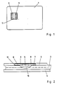
- FIG. 1 and 2 show an identification card consisting of several layers, in which a carrier element 11 is implanted in a suitable recess.
- the contact surfaces 9 lying on the card surface are electrically connected to a circuit 5.
- the card consists of a core layer 3 and two cover layers 2 and 4.
- the carrier element 11 consists of a substrate 8, on one side of which the contact areas 9 are located, which are connected via conductor tracks to one side of the substrate opposite the contact areas arranged IC module 5 are connected. At least the IC module 5 is surrounded by a resin drop 10.
- the top and core layers are provided with corresponding cutouts.
- the outline of the recess of the cover layer 2 is adapted to the size of the substrate 8, that of the core layer 3 is adapted to the size of the resin drop 10 in its outline.
- the card shown in the figures was laminated using heat and pressure.
- the substrate is connected to the core layer 3 with the aid of a hot-melt layer 7.
- the core layer 3 can be multilayered using a hot lamination process, such as by a dashed line in FIG 2, wherein the layers have recesses of different sizes, adapted to the shape of the resin drop 10.
- the core layers will seamlessly connect to the resin drops due to the softening during lamination.
- a cavity can form in the area of the resin drop, which remains free or can also be filled with a suitable material.
- a hot, but also a pressure sensitive adhesive can be used.
- the IC component 5 indicated in the resin drop 10 can be connected to the contact surfaces of the carrier element in various ways.
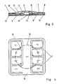
- FIG. 3 and 4 show an exemplary embodiment of the carrier element 11 roughly outlined in FIG. 2. It consists of three layers; a conductive layer 15, from which the contact design with the contact surfaces 9 is etched, a substrate 8, for example made of polyimide, and a hot-melt adhesive layer 7.
- the IC module 5 is connected directly to the conductive layer in a recess 13 in the substrate 8, for example with the aid of an adhesive.
- the recess 16 delimiting the casting compound 10 in the hot-melt adhesive layer 7 is of such a size that the IC component 5, the conductor tracks 6 and the connection points lying in the recesses 12 between the conductor tracks 6 and the contact surfaces 9 are enclosed in the casting compound 10.
- the recess 16 of the adhesive layer 7 which delimits the casting compound and prevents the casting compound from flowing off in the liquid phase, can be significantly smaller in thickness than the thickness of the casting cover in the region of the IC module or the connecting wires.
- a hardening resin is preferably used as the casting compound.
- the viscosity and amount of the casting compound are set so that the desired total thickness of the carrier element is not exceeded, but on the other hand all sensitive elements and connection points are protected in the casting compound.
- the areal expansion of the cast cover is dependent on the position of the cutouts 12 and the associated conductor track routing to the contact surfaces.
- the cutouts 12 will therefore be arranged as close as possible in the vicinity of the IC module 5 so that the cutout 16 in the adhesive layer 7 is correspondingly small and the remaining adhesive area is as large as possible.
- the hot-melt adhesive layer used in the described embodiment can also be applied together with a protective layer which is removed before or after the application of the casting compound. In this way, a clean adhesive surface is guaranteed in a simple manner during the manufacture of the carrier elements.
Landscapes
- Engineering & Computer Science (AREA)
- Computer Hardware Design (AREA)
- Microelectronics & Electronic Packaging (AREA)
- Physics & Mathematics (AREA)
- General Physics & Mathematics (AREA)
- Theoretical Computer Science (AREA)
- Credit Cards Or The Like (AREA)
- Road Signs Or Road Markings (AREA)
- Structures Or Materials For Encapsulating Or Coating Semiconductor Devices Or Solid State Devices (AREA)
- Solid-Sorbent Or Filter-Aiding Compositions (AREA)
Abstract
Description
- Die Erfindung betrifft ein Trägerelement mit einem oder mehreren integrierten Schaltkreisen zum Einbau einer Ausweiskarte, bestehend aus einem Substrat, auf dessen Oberflächen mehrere Kontaktflächen vorgesehen sind, die über Leiterbahnen mit den entsprechenden Anschlußpunkten eines in einer Aussparung des Substrats oder auf dem Substrat angeordnet integrierten Schaltkreises verbunden sind, mit einer Gußmasse, die zumindest den integrierten Schaltkreis umgibt und vor mechanischen Belastungen schützt und mit einem die Gußmasse begrenzenden Rahmen.
- Derartige Trägerelemente werden beispielsweise in Identifikations-, Kredit- oder Buchungskarten und dergleichen eingebaut.
- Zur rationellen und damit kostengünstigen Herstellung dieser Karten wird vorzugsweise ein Halbfabrikat verwendet, bei dem auf einem mit Leiterbahnen versehenen Träger ein oder mehrere integrierte Bausteine montiert sind. Bei der Kartenherstellung wird dieses sogenannte Trägerelement in eine passend geformte Aussparung einer Karte eingesetzt. Um beim Einbau des Trägerelements in eine Karte einen ausreichend festen Sitz in der vorgesehenen Kartenöffnung zu erreichen, wird das Trägerelement mit einem Kleber in der Öffnung fixiert.
- Es ist in diesem Zusammenhang bereits bekannt (EP-A1 201 952), Trägerelemente zur Befestigung in einer Ausweiskarte mit einer Haftkleberschicht zu versehen. Jedes Trägerelement besteht aus einem mit der Haftkleberschicht versehenen Substrat, auf dem ein IC-Baustein über Leiterbahnen (Golddrähte) mit Kontaktflächen verbunden ist. Die einzelnen Schichten des Trägerelements werden aus Endlosfilmen hergestellt. Die Haftkleberschicht ist, wie üblich, mit einer Schutzschicht versehen. Haftkleberschicht und Schutzschicht überdecken das Trägerelement mit Ausnahme des Bereichs, in dem sich IC-Baustein und Leiterbahnen befinden. Vor dem Einbau des Trägerelements in eine Karte wird die Schutzschicht von der Haftkleberschicht entfernt.
- Um Schaltkreis und Leiterbahnen gegen chemische Einflüsse zu schützen, werden die Trägerelemente, solange sie noch im Endlosformat vorliegen, großflächig mit einer 10 bis 50 µm dünnen Lackschicht besprüht, die den IC-Baustein, die Leiterbahnen und die Schutzschicht gleichmaßig überzieht.
- Bei dem vorgeschlagenen Verfahren können die Trägerelemente prinzipiell nur mit einer sehr dünnen Lackschicht besprüht werden, da auch die wieder zu entfernende Schutzschicht verfahrensbedingt von der Lackschicht überzogen ist. Bei dickeren Lackschichten ist durch das Abziehen der Schutzschicht eine Beschädigung der Lackschicht im Bereich der Leiterbahnen und damit eine Beschädigung der Leiterbahnen selbst nicht zu vermeiden.
- Mit dem bekannten Vorschlag mag daher ein ausreichender Schutz gegen chemische Einflüsse erzielbar sein. Auf keinen Fall sind IC-Baustein und Leiterbahnen, die sowohl während der Herstellung als auch im Gebrauch der Karte häufigen Biege- und Druckbelastungen ausgesetzt sind, mit dem vorgeschlagenen Verfahren ausreichend gegen mechanische Belastungen geschützt. Um diesbezüglich einen wirkungsvollen mechanischen Schutz zu erreichen, müssen daher andere Maßnahmen ergriffen werden.
- Die EP-OS 0 107 061 beschreibt beispielsweise ein Trägerelement, das aus einer mit Leiterbahnen versehenen Folie besteht. Um den IC-Baustein mit Hilfe üblicher Drahtverbindungen kontaktieren zu können und trotzdem die geforderte Kartendicke nicht zu überschreiten, wird der IC-Baustein in einem Stanzloch dieser Folie montiert. Zum Schutz der gegen mechanische Beanspruchungen empfindlichen Elemente wird hier auf der Oberseite der Folie zusätzlich ein ringförmiger Begrenzungskörper aufgebracht, der den IC-Baustein und die Drahtverbindungen einschließt und der mit einem Harz gefüllt wird. Nach dem Aushärten des Harzes wird die Oberseite des Begrenzungskörpers gemeinsam mit der Harzmasse abgeschliffen, damit die geforderte Dicke der herzustellenden Karte auch tatsächlich erreicht werden kann.
- Bei diesem bekannten Vorschlag ist es vor allem im Hinblick auf eine kostengünstige Herstellung eines Trägerelements nachteilig, daß in einem separaten und zusätzlichen Arbeitsgang ein Rahmen aufgebracht werden muß, um ein Auslaufen einer zu Schutzzwecken auf den IC-Baustein aufzubringenden, aushärtenden Gußmasse zu verhindern. Andererseits ist ein begrenzendes Element notwendig, um die Gußmasse auf einen definierten Bereich zu begrenzen und mit vorbestimmter Dicke auf die zu schützenden Elemente aufbringen zu können. Ohne ein begrenzendes Element kann die Gußmasse, wenn überhaupt, nur mit Überdicke auf die zu schützenden Teile aufgebracht werden. Vor dem Einbau des Trägerelements in eine Ausweiskarte mit vorbestimmter Dicke muß dann aber das überschüssige Gußmaterial, beispielsweise durch Abschleifen, entfernt werden.
- Der Erfindung liegt nun die Aufgabe zugrunde, ein Trägerelement mit IC-Baustein zum Einbau in Ausweiskarten zu schaffen, bei dem trotz rationeller und kostengünstiger Herstellung die empfindlichen Bauteile sehr gut gegen mechanische Belastungen geschützt sind.
- Gelöst wird diese Aufgabe gemäß dem kennzeichnenden Teil des Hauptanspruchs.
- Ein bewährtes Verfahren zum Einbau von Trägerelementen in Ausweiskarten besteht darin, daß das Trägerelement mit Hilfe einer Klebeschicht mit dem Kartenkörper verbunden wird.
- Die Erfindung zeichnet sich nun gegenüber dem genannten Stand der Technik vor allem dadurch aus, daß eine Aussparung in einer zum Einbau eines Trägerelements in eine Ausweiskarte ohnehin notwendigen Klebeschicht als Rahmen für die schützende Gußmasse dient. Dabei hat sich überraschend gezeigt, daß selbst bei einer sehr dünnen Klebeschicht die Funktion eines Begrenzungsrahmens gewährleistet ist. Diese Doppelfunktion der Klebeschicht erspart also das zusätzliche Aufbringen eines Rahmens, ohne auf die Vorteile der bekannten Begrenzungsrahmen verzichten zu müssen. Durch die Gußabdeckung kann der IC-Baustein allein oder zusammen mit den Verbindungsdrähten wirkungsvoll gegen mechanische und auch chemische Einflüsse geschützt werden, obwohl auf die zusätzliche Aufbringung eines speziellen Begrenzungsrahmens verzichtet werden kann. Zur Herstellung des Trägerelements sind also weniger Herstellungsschritte nötig. Die genaue Dosierung der Gußmasse bei gleichbleibender Größe der Aussparung (Stanzloch im Klebefilm) erlaubt zum einen den sparsamen Einsatz von Gußmasse und zum anderen die Herstellung eines Trägerelements mit einer gut einstellbaren und gleichbleibenden Dicke.
- Die Trägerelemente werden im allgemeinen aus Endlosfilmen hergestellt. Hierbei werden die einzelnen Schichten des späteren Trägerelements als Endlosfilme von je einer Filmrolle abgespult und passergenau zusammengebracht. Die so produzierten Tägerelemente müssen dann zum Einbau in eine Ausweiskarte lediglich aus dem Filmlaminat ausgestanzt und in die Karte eingesetzt werden. Ein nach diesem Prinzip arbeitendes Herstellungsverfahren ist beispielsweise in der DE-OS 36 39 630 beschrieben.
- Um die schützende Gußmasse auf das Trägerelement dosiert aufbringen zu können, ist es bei Anwendung des bekannten Verfahrens demnach lediglich erforderlich, den auf einer der Filmrollen befindlichen Klebeschicht-Film in regelmäßigen Abständen mit einer geeigneten Aussparung zu versehen. Dies kann auf einfache Weise entweder vorab oder auch in dem oben geschilderten Verfahrensablauf geschehen.
- In einer bevorzugten Ausführungsform der Erfindung besteht das den IC-Baustein tragende Substrat aus einem Kunststoffilm aus Polyester, Polyimid oder einem ähnlichen Material. Der Film ist ganzflächig mit einer leitenden Schicht überzogen, aus der das gewünschte Konkaktdesign ausgeätzt ist. Für den IC-Baustein und die Zuführungen der Leiterbahnen zu den Kontaktflächen sind im Film mehrere Aussparungen vorgesehen. Auf der den Kontaktflächen gegenüberliegenden Seite des Films ist eine Heißkleberschicht aufgebracht, die eine Aussparung solcher Größe aufweist, daß der IC-Baustein und die den Kontaktflächen zugeordneten Aussparungen frei zugängig sind. Dieser frei zugängige Bereich ist mit einem geeigneten Gußharz gefüllt, wobei der Rand der Aussparung in der Heißkleberschicht die Harzmasse während des Auftragens in der flüssigen Phase begrenzt. Art des Harzmaterials, Mengendosierung und weitere in diesem Zusammenhang dem Fachmann bekannte Parameter sind so gewählt, daß einerseits IC-Baustein und Leiterbahnen sicher eingeschlossen sind und andererseits die Gesamtanordnung eine vorbestimmte Dicke nicht übersteigt.
- Weitere Vorteile und Weiterbildungen der Erfindung ergeben sich aus den Unteransprüchen sowie den Ausführungsbeispielen, die nachfolgend anhand der Fig. beschrieben werden.
- Darin zeigen:
- Fig. 1 eine Ausweiskarte mit eingelagertem IC-Baustein in der Aufsicht,
- Fig. 2 die Ausweiskarte nach Fig. 1 im Schnitt,
- Fig. 3 ein Trägerelement im Schnitt,
- Fig. 4 das Trägerelement aus Fig. 3 in der Aufsicht.
- Die Fig. 1 und 2 zeigen eine aus mehreren Schichten bestehende Ausweiskarte, bei der in einer geeigneten Aussparung ein Trägerelement 11 implantiert ist. Die an der Kartenoberfläche liegenden Kontaktflächen 9 sind elektrisch mit einem Schaltkreis 5 verbunden.
- In der gezeigten beispielhaften Ausführungsform besteht die Karte aus einer Kernschicht 3 sowie zwei Deckschichten 2 und 4. Das Trägerelement 11 besteht aus einem Substrat 8, auf dessen einer Seite die Kontaktflächen 9 liegen, die über Leiterbahnen mit einem auf der den Kontaktflächen gegenüberliegenden Seite des Substrats angeordneten IC-Baustein 5 verbunden sind. Zumindest der IC-Baustein 5 ist von einem Harztropfen 10 umgeben. Um das Trägerelement in eine Ausweiskarte einbetten zu können, sind Deck- und Kernschicht mit entsprechenden Aussparungen versehen. Die Aussparung der Deckschicht 2 ist in ihrem Umriß der Größe des Substrats 8, die der Kernschicht 3 in ihrem Umriß der Größe des Harztropfens 10 angepaßt.
- Die in den Fig. gezeigte Karte wurde unter Anwendung von Wärme und Druck laminiert. Während des Laminiervorgangs wird dabei das Substrat mit Hilfe einer Heißkleberschicht 7 mit der Kernschicht 3 verbunden. Die Kernschicht 3 kann bei Anwendung eines Heißlaminierverfahrens mehrschichtig sein, wie durch eine strichlierte Linie in der Fig. 2 angedeutet, wobei die Schichten unterschiedlich große, der Form des Harztropfens 10 angepaßte, Aussparungen aufweisen. Bei der fertiggestellten Karte werden die Kernschichten aufgrund der Erweichung während des Laminierens lückenlos an den Harztropfen anschließen. Bei anderen Herstellungstechniken (z. B. Einbau des Trägerelements in eine bereits laminierte Karte) kann im Bereich des Harztropfens ein Hohlraum entstehen, der frei bleibt oder auch mit einem geeigneten Material ausgefüllt werden kann.
- Bei der letztgenannten Herstellungsmethode kann ein Heiß-, aber auch ein Haftkleber verwendet werden. Der im Harztropfen 10 angedeutete IC-Baustein 5 kann auf verschiedene Arten mit den Kontaktflächen des Trägerelements verbunden sein.
- Fig. 3 und 4 zeigen eine beispielhafte Ausführungsform des in Fig. 2 grob skizzierten Trägerelements 11. Es besteht aus drei Schichten; einer leitenden Schicht 15, aus der das Kontaktdesign mit den Kontaktflächen 9 ausgeätzt ist, einem Substrat 8, beispielsweise aus Polyimid und einer Heißkleberschicht 7. Die im allgemeinen aus Kupfer hergestellten, vorzugsweise mit einer Nickel- und Goldauflage überzogenen Kontaktflächen 9 berühren sich nicht.
- In dem gezeigten Ausführungsbeispiel ist der IC-Baustein 5 in einer Aussparung 13 des Substrats 8 direkt mit der leitenden Schicht, beispielsweise mit Hilfe eines Klebstoffs, verbunden.
- Weitere Aussparungen 12 im Substrat sind derart plaziert, daß sie - gesehen von der Seite des Trägerelements, auf der der IC-Baustein angeordnet ist - den Zugang zu den Kontaktflächen 9 ermöglichen. So kann auf einfache Weise eine elektrische Verbindung hergestellt werden zwischen den Anschlußpunkten des IC-Bausteins 5 und den entspre chenden Kontaktflächen 9. In dem gezeigten Ausführungsbeispiel wurde die sogenannte Drahtbondtechnik eingesetzt, bei der feine Golddrähte 6 die elektrische Verbindung herstellen.
- Die die Gußmasse 10 begrenzende Aussparung 16 in der Heißkleberschicht 7 hat eine solche Größe, daß der IC-Baustein 5, die Leiterbahnen 6 und die in den Aussparungen 12 liegenden Verbindungspunkte zwischen den Leiterbahnen 6 und den Kontaktflächen 9 in der Gußmasse 10 eingeschlossen sind. Die die Gußmasse begrenzende Aussparung 16 der Klebeschicht 7, die das Abfließen der Gußmasse in der flüssigen Phase verhindert, kann in der Dicke deutlich geringer sein, als die Dicke der Gußabdeckung im Bereich des IC-Bausteins oder der Verbindungsdrähte. Als Gußmasse wird vorzugsweise ein aushärtendes Harz verwendet. Viskosität und Menge der Gußmasse sind so eingestellt, daß die gewünschte Gesamtdicke des Trägerelements nicht überschritten wird, aber andererseits alle empfindlichen Elemente und Verbindungsstellen geschützt in der Gußmasse liegen. Die flächenmäßige Ausdehnung der Gußabdeckung ist abhängig von der Lage der Aussparungen 12 und der damit verbundenen Leiterbahnführung zu den Kontaktflächen. Man wird daher die Aussparungen 12 möglichst nahe in der Umgebung des IC-Bausteins 5 anordnen, damit die Aussparung 16 in der Klebeschicht 7 entsprechend klein und die verbleibende Klebefläche möglichst groß ist.
- Die in der beschriebenen Ausführungsform verwendete Heißkleberschicht kann auch zusammen mit einer Schutzschicht aufgebracht werden, die vor oder auch nach dem Aufbringen der Gußmasse abgezogen wird. So wird bei der Herstellung der Trägerelemente auf einfache Art und Weise eine saubere Klebeoberfläche garantiert.
Claims (4)
dadurch gekennzeichnet, daß das Substrat (8) auf der den Kontaktflächen (9) gegenüberliegenden Seite eine zur Verbindung des Substrats (8) mit einem Kartenkörper dienende Klebeschicht (7) aufweist und diese Klebeschicht (7) zumindest im Bereich des integrierten Schaltkreises (5) eine Aussparung (16) aufweist, die den Begrenzungsrahmen für die Gußmasse bildet.
dadurch gekennzeichnet, daß das Material der Gußmasse (10) in der Menge derart dosiert ist, daß sie im Bereich des IC-Bausteins (5) unter Tropfenbildung die Dicke der Klebeschicht (7) um ein Vielfaches übersteigt.
dadurch gekennzeichnet, daß die Klebeschicht eine Heißkleberschicht (7) ist.
dadurch gekennzeichnet, daß auf einem mit IC-Baustein (5), Leiterbahnen (6) und Kontaktflächen (9) vorbereiteten Substrat (8) eine Klebeschicht (7) aufgebracht wird, die im Bereich des IC-Bausteins (5) eine Aussparung (16) aufweist und daß anschließend der durch die Aussparung gebildete Bereich mit einer Gußmasse (10) gefüllt wird, wobei die Dosierung der Gußmasse (10) derart eingestellt ist, daß einerseits der IC-Baustein (5) vollständig eingeschlossen ist und andererseits die Klebeschicht (7) vollständig frei bleibt.
Priority Applications (1)
| Application Number | Priority Date | Filing Date | Title |
|---|---|---|---|
| AT88111437T ATE73945T1 (de) | 1987-07-16 | 1988-07-15 | Traegerelement zum einbau in ausweiskarten. |
Applications Claiming Priority (2)
| Application Number | Priority Date | Filing Date | Title |
|---|---|---|---|
| DE3723547 | 1987-07-16 | ||
| DE3723547A DE3723547C2 (de) | 1987-07-16 | 1987-07-16 | Trägerelement zum Einbau in Ausweiskarten |
Publications (2)
| Publication Number | Publication Date |
|---|---|
| EP0299530A1 true EP0299530A1 (de) | 1989-01-18 |
| EP0299530B1 EP0299530B1 (de) | 1992-03-18 |
Family
ID=6331714
Family Applications (1)
| Application Number | Title | Priority Date | Filing Date |
|---|---|---|---|
| EP88111437A Expired - Lifetime EP0299530B1 (de) | 1987-07-16 | 1988-07-15 | Trägerelement zum Einbau in Ausweiskarten |
Country Status (7)
| Country | Link |
|---|---|
| US (1) | US5027190A (de) |
| EP (1) | EP0299530B1 (de) |
| JP (1) | JP2676619B2 (de) |
| AT (1) | ATE73945T1 (de) |
| DE (2) | DE3723547C2 (de) |
| ES (1) | ES2030800T3 (de) |
| HK (1) | HK54295A (de) |
Cited By (10)
| Publication number | Priority date | Publication date | Assignee | Title |
|---|---|---|---|---|
| FR2670930A1 (fr) * | 1990-12-21 | 1992-06-26 | Bull Cp8 | Procede de realisation du module electronique d'un objet portatif tel qu'une carte a microcircuits, module et cartes obtenus par la mise en óoeuvre du procede. |
| WO1992013318A1 (de) * | 1991-01-21 | 1992-08-06 | Telbus Gesellschaft Für Elektronische Kommunikations-Systeme Mbh | Trägerelement für integrierte halbleiter-schaltkreise, insbesondere zum einbau in chip-karten |
| DE4126874C1 (de) * | 1991-08-14 | 1992-08-13 | Orga Kartensysteme Gmbh, 6072 Dreieich, De | |
| EP0521502A1 (de) * | 1991-07-03 | 1993-01-07 | GAO Gesellschaft für Automation und Organisation mbH | Verfahren zum Einbau eines Trägerelements |
| DE4427802C1 (de) * | 1994-08-05 | 1995-10-26 | Beiersdorf Ag | Thermoaktivierbare Klebfolie zur Herstellung eines Datenträgers |
| EP0643366A3 (de) * | 1993-08-10 | 1996-01-03 | Giesecke & Devrient Gmbh | Elektronisches Modul für Karten und Herstellung eines solchen Moduls. |
| FR2769110A1 (fr) * | 1997-09-26 | 1999-04-02 | Gemplus Card Int | Procede de fabrication d'un module ou etiquette electronique, module ou etiquette obtenue et support comportant un tel module ou etiquette |
| DE4040770C2 (de) * | 1990-12-19 | 1999-11-11 | Gao Ges Automation Org | Datenträger mit integriertem Schaltkreis |
| EP1615166A1 (de) * | 2004-07-07 | 2006-01-11 | Axalto S.A. | Trägerband für Chipmodule und Herstellungsverfahren für Chipkarten |
| CN100452089C (zh) * | 1997-09-26 | 2009-01-14 | 格姆普拉斯公司 | 电子模块 |
Families Citing this family (46)
| Publication number | Priority date | Publication date | Assignee | Title |
|---|---|---|---|---|
| DE4105869C2 (de) * | 1991-02-25 | 2000-05-18 | Edgar Schneider | IC-Karte und Verfahren zu ihrer Herstellung |
| DE4209184C1 (de) * | 1992-03-21 | 1993-05-19 | Orga Kartensysteme Gmbh, 6072 Dreieich, De | |
| US5796164A (en) * | 1993-05-11 | 1998-08-18 | Micromodule Systems, Inc. | Packaging and interconnect system for integrated circuits |
| JPH0737049A (ja) * | 1993-07-23 | 1995-02-07 | Toshiba Corp | 外部記憶装置 |
| DE4340847A1 (de) * | 1993-11-26 | 1995-06-01 | Optosys Gmbh Berlin | Chipmodul und Verfahren zur Herstellung eines Chipmoduls |
| FR2721732B1 (fr) * | 1994-06-22 | 1996-08-30 | Solaic Sa | Carte à mémoire sans contact dont le circuit électronique comporte un module. |
| DE4423575A1 (de) | 1994-07-05 | 1996-01-11 | Giesecke & Devrient Gmbh | Datenträger mit einem Modul mit integriertem Schaltkreis |
| DE4443767A1 (de) * | 1994-12-08 | 1996-06-13 | Giesecke & Devrient Gmbh | Elektronisches Modul und Datenträger mit elektrischem Modul |
| DE19502157B4 (de) * | 1995-01-25 | 2011-07-21 | Sagem Orga GmbH, 33106 | Trägerelement für einen IC-Baustein zum Einbau in Chipkarten |
| DE19512725C1 (de) * | 1995-04-05 | 1996-09-12 | Orga Kartensysteme Gmbh | Ausweiskarte o.dgl. in Form einer Chipkarte |
| EP0766197A4 (de) * | 1995-04-13 | 1999-12-29 | Dainippon Printing Co Ltd | Chipkarte und -modul |
| US5677521A (en) * | 1995-06-29 | 1997-10-14 | Garrou; Elizabeth B. | Personal identification and credit information system and method of performing transaction |
| DE29510947U1 (de) * | 1995-07-06 | 1995-09-14 | Stocko Metallwarenfabriken Henkels Und Sohn Gmbh & Co, 42327 Wuppertal | Kontaktfeldbaugruppe zur Anordnung auf einer Kontaktiereinheit |
| DE19539181C2 (de) * | 1995-10-20 | 1998-05-14 | Ods Gmbh & Co Kg | Chipkartenmodul sowie entsprechendes Herstellungsverfahren |
| ES2149000T3 (es) * | 1996-08-02 | 2000-10-16 | Schlumberger Systems & Service | Tarjeta de circuito integrado con conexion mixta. |
| DE19632813C2 (de) * | 1996-08-14 | 2000-11-02 | Siemens Ag | Verfahren zur Herstellung eines Chipkarten-Moduls, unter Verwendung dieses Verfahrens hergestellter Chipkarten-Modul und diesen Chipkarten-Modul enthaltende Kombi-Chipkarte |
| US5847445A (en) * | 1996-11-04 | 1998-12-08 | Micron Technology, Inc. | Die assemblies using suspended bond wires, carrier substrates and dice having wire suspension structures, and methods of fabricating same |
| DE19703990A1 (de) * | 1997-02-03 | 1998-08-06 | Giesecke & Devrient Gmbh | Modular aufgebauter, elektronischer Datenträger |
| KR100431501B1 (ko) * | 1997-06-05 | 2004-10-02 | 삼성전자주식회사 | 고전력 패키지 구조 및 제조 방법 |
| CN1110770C (zh) * | 1997-06-23 | 2003-06-04 | 罗姆股份有限公司 | 智能卡用模块、智能卡及智能卡用模块的制造方法 |
| JP3883652B2 (ja) * | 1997-06-23 | 2007-02-21 | 大日本印刷株式会社 | 板状枠体付きicキャリアとその製造方法 |
| FR2769130B1 (fr) * | 1997-09-30 | 2001-06-08 | Thomson Csf | Procede d'enrobage d'une puce electronique et carte electronique comportant au moins une puce enrobee selon ce procede |
| FR2769390B1 (fr) * | 1997-10-08 | 2003-02-14 | Gemplus Card Int | Procede de fabrication de cartes a puce aptes a assurer un fonctionnement a contact et sans contact, et de cartes a puce sans contact |
| US6241153B1 (en) * | 1998-03-17 | 2001-06-05 | Cardxx, Inc. | Method for making tamper-preventing, contact-type, smart cards |
| FR2785072B1 (fr) * | 1998-10-23 | 2001-01-19 | St Microelectronics Sa | Circuit electronique autocollant |
| US6179210B1 (en) * | 1999-02-09 | 2001-01-30 | Motorola, Inc. | Punch out pattern for hot melt tape used in smartcards |
| FR2793331B1 (fr) * | 1999-05-06 | 2001-08-10 | Oberthur Card Systems Sas | Procede de fabrication d'une carte a microcircuit |
| DE10024376A1 (de) * | 2000-05-17 | 2001-12-06 | Infineon Technologies Ag | Halbleiterbauelement und Verfahren zu dessen Herstellung |
| DE20100158U1 (de) | 2001-01-05 | 2002-05-08 | Bundesdruckerei GmbH, 10969 Berlin | Identifikations- und Sicherheitskarte aus laminierten und/oder gespritzten Kunststoffen |
| CA2601512A1 (en) * | 2005-03-23 | 2006-09-28 | Cardxx, Inc. | Method for making advanced smart cards with integrated electronics using isotropic thermoset adhesive materials with high quality exterior surfaces |
| JP2007133802A (ja) * | 2005-11-14 | 2007-05-31 | Dainippon Printing Co Ltd | Icカードおよびicカード用icモジュール |
| USD571810S1 (en) * | 2006-06-20 | 2008-06-24 | Kabushiki Kaisha Toshiba | Module with built-in integrated circuits for use with IC cards |
| US8649820B2 (en) | 2011-11-07 | 2014-02-11 | Blackberry Limited | Universal integrated circuit card apparatus and related methods |
| USD703208S1 (en) | 2012-04-13 | 2014-04-22 | Blackberry Limited | UICC apparatus |
| US8936199B2 (en) | 2012-04-13 | 2015-01-20 | Blackberry Limited | UICC apparatus and related methods |
| USD701864S1 (en) * | 2012-04-23 | 2014-04-01 | Blackberry Limited | UICC apparatus |
| US9647997B2 (en) | 2013-03-13 | 2017-05-09 | Nagrastar, Llc | USB interface for performing transport I/O |
| USD758372S1 (en) * | 2013-03-13 | 2016-06-07 | Nagrastar Llc | Smart card interface |
| US9888283B2 (en) | 2013-03-13 | 2018-02-06 | Nagrastar Llc | Systems and methods for performing transport I/O |
| USD759022S1 (en) * | 2013-03-13 | 2016-06-14 | Nagrastar Llc | Smart card interface |
| USD729808S1 (en) * | 2013-03-13 | 2015-05-19 | Nagrastar Llc | Smart card interface |
| USD780763S1 (en) | 2015-03-20 | 2017-03-07 | Nagrastar Llc | Smart card interface |
| USD864968S1 (en) | 2015-04-30 | 2019-10-29 | Echostar Technologies L.L.C. | Smart card interface |
| JP1633612S (de) * | 2018-02-01 | 2019-06-10 | ||
| USD930000S1 (en) | 2018-10-12 | 2021-09-07 | Huawei Technologies Co., Ltd. | Memory card |
| USD983261S1 (en) | 2019-12-20 | 2023-04-11 | Capital One Services, Llc | Vented laminated card |
Citations (5)
| Publication number | Priority date | Publication date | Assignee | Title |
|---|---|---|---|---|
| FR2337381A1 (fr) * | 1975-12-31 | 1977-07-29 | Honeywell Bull Soc Ind | Carte portative pour systeme de traitement de signaux electriques et procede de fabrication de cette carte |
| FR2520541A1 (fr) * | 1982-01-22 | 1983-07-29 | Flonic Sa | Procede d'insertion d'un circuit integre dans une carte a memoire et carte obtenue suivant ce procede |
| EP0107061A2 (de) * | 1982-09-27 | 1984-05-02 | Philips Patentverwaltung GmbH | Informationskarte und Verfahren zu ihrer Herstellung |
| FR2548857A1 (fr) * | 1983-07-04 | 1985-01-11 | Cortaillod Cables Sa | Procede de fabrication en continu d'une carte imprimee |
| EP0201952B1 (de) * | 1985-04-12 | 1990-09-19 | Philips Composants | Verfahren und Einrichtung zur Herstellung einer elektronischen Identifikationskarte |
Family Cites Families (4)
| Publication number | Priority date | Publication date | Assignee | Title |
|---|---|---|---|---|
| US4216577A (en) * | 1975-12-31 | 1980-08-12 | Compagnie Internationale Pour L'informatique Cii-Honeywell Bull (Societe Anonyme) | Portable standardized card adapted to provide access to a system for processing electrical signals and a method of manufacturing such a card |
| US4222516A (en) * | 1975-12-31 | 1980-09-16 | Compagnie Internationale Pour L'informatique Cii-Honeywell Bull | Standardized information card |
| JPS57207357A (en) * | 1981-06-17 | 1982-12-20 | Asahi Glass Co Ltd | Component part holder |
| DE3639630A1 (de) * | 1986-11-20 | 1988-06-01 | Gao Ges Automation Org | Datentraeger mit integriertem schaltkreis und verfahren zur herstellung desselben |
-
1987
- 1987-07-16 DE DE3723547A patent/DE3723547C2/de not_active Expired - Fee Related
-
1988
- 1988-07-15 JP JP63176870A patent/JP2676619B2/ja not_active Expired - Fee Related
- 1988-07-15 ES ES198888111437T patent/ES2030800T3/es not_active Expired - Lifetime
- 1988-07-15 EP EP88111437A patent/EP0299530B1/de not_active Expired - Lifetime
- 1988-07-15 DE DE8888111437T patent/DE3869248D1/de not_active Expired - Fee Related
- 1988-07-15 AT AT88111437T patent/ATE73945T1/de not_active IP Right Cessation
-
1990
- 1990-09-12 US US07/581,394 patent/US5027190A/en not_active Expired - Lifetime
-
1995
- 1995-04-11 HK HK54295A patent/HK54295A/xx not_active IP Right Cessation
Patent Citations (5)
| Publication number | Priority date | Publication date | Assignee | Title |
|---|---|---|---|---|
| FR2337381A1 (fr) * | 1975-12-31 | 1977-07-29 | Honeywell Bull Soc Ind | Carte portative pour systeme de traitement de signaux electriques et procede de fabrication de cette carte |
| FR2520541A1 (fr) * | 1982-01-22 | 1983-07-29 | Flonic Sa | Procede d'insertion d'un circuit integre dans une carte a memoire et carte obtenue suivant ce procede |
| EP0107061A2 (de) * | 1982-09-27 | 1984-05-02 | Philips Patentverwaltung GmbH | Informationskarte und Verfahren zu ihrer Herstellung |
| FR2548857A1 (fr) * | 1983-07-04 | 1985-01-11 | Cortaillod Cables Sa | Procede de fabrication en continu d'une carte imprimee |
| EP0201952B1 (de) * | 1985-04-12 | 1990-09-19 | Philips Composants | Verfahren und Einrichtung zur Herstellung einer elektronischen Identifikationskarte |
Cited By (12)
| Publication number | Priority date | Publication date | Assignee | Title |
|---|---|---|---|---|
| DE4040770C2 (de) * | 1990-12-19 | 1999-11-11 | Gao Ges Automation Org | Datenträger mit integriertem Schaltkreis |
| FR2670930A1 (fr) * | 1990-12-21 | 1992-06-26 | Bull Cp8 | Procede de realisation du module electronique d'un objet portatif tel qu'une carte a microcircuits, module et cartes obtenus par la mise en óoeuvre du procede. |
| WO1992013318A1 (de) * | 1991-01-21 | 1992-08-06 | Telbus Gesellschaft Für Elektronische Kommunikations-Systeme Mbh | Trägerelement für integrierte halbleiter-schaltkreise, insbesondere zum einbau in chip-karten |
| EP0521502A1 (de) * | 1991-07-03 | 1993-01-07 | GAO Gesellschaft für Automation und Organisation mbH | Verfahren zum Einbau eines Trägerelements |
| DE4126874C1 (de) * | 1991-08-14 | 1992-08-13 | Orga Kartensysteme Gmbh, 6072 Dreieich, De | |
| EP0643366A3 (de) * | 1993-08-10 | 1996-01-03 | Giesecke & Devrient Gmbh | Elektronisches Modul für Karten und Herstellung eines solchen Moduls. |
| DE4427802C1 (de) * | 1994-08-05 | 1995-10-26 | Beiersdorf Ag | Thermoaktivierbare Klebfolie zur Herstellung eines Datenträgers |
| FR2769110A1 (fr) * | 1997-09-26 | 1999-04-02 | Gemplus Card Int | Procede de fabrication d'un module ou etiquette electronique, module ou etiquette obtenue et support comportant un tel module ou etiquette |
| WO1999017253A1 (fr) * | 1997-09-26 | 1999-04-08 | Gemplus S.C.A. | Procede de fabrication d'un module ou etiquette electronique, module ou etiquette obtenu et support comportant un tel module ou etiquette |
| US6446874B1 (en) | 1997-09-26 | 2002-09-10 | Gemplus S.A., Inc. | Method of fabricating an electronic module or label, module or label obtained and medium including a module or label of this kind |
| CN100452089C (zh) * | 1997-09-26 | 2009-01-14 | 格姆普拉斯公司 | 电子模块 |
| EP1615166A1 (de) * | 2004-07-07 | 2006-01-11 | Axalto S.A. | Trägerband für Chipmodule und Herstellungsverfahren für Chipkarten |
Also Published As
| Publication number | Publication date |
|---|---|
| US5027190A (en) | 1991-06-25 |
| ATE73945T1 (de) | 1992-04-15 |
| HK54295A (en) | 1995-04-21 |
| DE3723547C2 (de) | 1996-09-26 |
| JP2676619B2 (ja) | 1997-11-17 |
| JPS6436496A (en) | 1989-02-07 |
| DE3723547A1 (de) | 1989-01-26 |
| EP0299530B1 (de) | 1992-03-18 |
| ES2030800T3 (es) | 1992-11-16 |
| DE3869248D1 (de) | 1992-04-23 |
Similar Documents
| Publication | Publication Date | Title |
|---|---|---|
| EP0299530B1 (de) | Trägerelement zum Einbau in Ausweiskarten | |
| DE68921179T2 (de) | Elektronisches Modul mit einer integrierten Schaltung für ein kleines tragbares Objekt, z.B. eine Karte oder ein Schlüssel und Herstellungsverfahren für solche Module. | |
| EP0484353B1 (de) | Trägerelement mit wenigstens einem integrierten schaltkreis, insbesondere zum einbau in chip-karten | |
| EP0268830B1 (de) | Datenträger mit integriertem Schaltkreis und Verfahren zur Herstellung desselben | |
| DE69512137T2 (de) | Herstellungsverfahren und Montage für IC-Karte. | |
| DE3688984T2 (de) | IC-Karte. | |
| EP2027600B1 (de) | Verfahren zum Einbetten zumindest eines Bauelements in einem Leiterplattenelement | |
| DE3586666T2 (de) | Karte mit ic-baustein und verfahren zur herstellung derselben. | |
| DE19911916B4 (de) | Verfahren zur Herstellung einer Halbleitervorrichtung mit Schutzlage | |
| EP0709805B1 (de) | Verfahren zur Herstellung von Datenträgern mit eingebetteten Elementen und Vorrichtung zur Durchführung des Verfahrens | |
| EP0919041B1 (de) | Verfahren zur herstellung eines chipkarten-moduls für eine kombi-chipkarte | |
| DE69832104T2 (de) | Verbindung durch Aufbringen eines dem Relief entsprechenden viskosen Produktes | |
| DE69824679T2 (de) | Kontaktlose elektronische Karte und Verfahren zur Herstellung einer solchen Karte | |
| DE10240461A1 (de) | Universelles Gehäuse für ein elektronisches Bauteil mit Halbleiterchip und Verfahren zu seiner Herstellung | |
| DE3149641A1 (de) | "eleketrische schaltungsplatte und verfahren zu ihrer herstellung" | |
| EP0591668A1 (de) | Verfahren zur Montage von integrierten Halbleiterschaltkreisen | |
| DE3111516A1 (de) | "ausweiskarte mit ic-baustein" | |
| DE602004004647T2 (de) | Verfahren zum zusammenbauen eines elektronischen komponent auf einem substrat | |
| EP4404101A2 (de) | Kartenförmiger datenträger sowie halbzeug und kontaktlayout dafür, und verfahren zur herstellung derselben | |
| AT515443B1 (de) | Verfahren zum Herstellen einer Leiterplatte sowie Leiterplatte | |
| DE19940480C2 (de) | Leiterbahnträgerschicht zur Einlaminierung in eine Chipkarte, Chipkarte mit einer Leiterbahnträgerschicht und Verfahren zur Herstellung einer Chipkarte | |
| DE19539181C2 (de) | Chipkartenmodul sowie entsprechendes Herstellungsverfahren | |
| DE4325458A1 (de) | Trägerelement für einen IC-Baustein | |
| EP0953186A1 (de) | Chipkartenmodul | |
| DE4022829A1 (de) | Tragbare speicherkarte |
Legal Events
| Date | Code | Title | Description |
|---|---|---|---|
| PUAI | Public reference made under article 153(3) epc to a published international application that has entered the european phase |
Free format text: ORIGINAL CODE: 0009012 |
|
| AK | Designated contracting states |
Kind code of ref document: A1 Designated state(s): AT BE CH DE ES FR GB IT LI LU NL SE |
|
| 17P | Request for examination filed |
Effective date: 19890619 |
|
| 17Q | First examination report despatched |
Effective date: 19910610 |
|
| GRAA | (expected) grant |
Free format text: ORIGINAL CODE: 0009210 |
|
| AK | Designated contracting states |
Kind code of ref document: B1 Designated state(s): AT BE CH DE ES FR GB IT LI LU NL SE |
|
| REF | Corresponds to: |
Ref document number: 73945 Country of ref document: AT Date of ref document: 19920415 Kind code of ref document: T |
|
| ET | Fr: translation filed | ||
| REF | Corresponds to: |
Ref document number: 3869248 Country of ref document: DE Date of ref document: 19920423 |
|
| GBT | Gb: translation of ep patent filed (gb section 77(6)(a)/1977) | ||
| ITF | It: translation for a ep patent filed | ||
| REG | Reference to a national code |
Ref country code: ES Ref legal event code: FG2A Ref document number: 2030800 Country of ref document: ES Kind code of ref document: T3 |
|
| PLBI | Opposition filed |
Free format text: ORIGINAL CODE: 0009260 |
|
| PLAB | Opposition data, opponent's data or that of the opponent's representative modified |
Free format text: ORIGINAL CODE: 0009299OPPO |
|
| 26 | Opposition filed |
Opponent name: GAO GESELLSCHAFT FUER AUTOMATION UND ORGANISATION Effective date: 19921217 |
|
| R26 | Opposition filed (corrected) |
Opponent name: PHILIPS ELECTRONICS N.V. Effective date: 19921217 |
|
| NLR1 | Nl: opposition has been filed with the epo |
Opponent name: PHILIPS ELECTRONICS N.V. |
|
| EPTA | Lu: last paid annual fee | ||
| EAL | Se: european patent in force in sweden |
Ref document number: 88111437.5 |
|
| PLBN | Opposition rejected |
Free format text: ORIGINAL CODE: 0009273 |
|
| STAA | Information on the status of an ep patent application or granted ep patent |
Free format text: STATUS: OPPOSITION REJECTED |
|
| 27O | Opposition rejected |
Effective date: 19950708 |
|
| NLR2 | Nl: decision of opposition | ||
| ZE | Nl: corrections to earlier entries in headings pe - xe |
Free format text: PAT.BUL.01/96 HEADING RE,SECTION 2,PAGE 104,105 AND 106;DECISIONS ON OPPOSITIONS "OPPOSITIE AFGEWEZEN.OCTROOI HERROEPEN" CORR. "OPPOSITIE AFGEWEZEN.OCTROOI GEHANDHAAFD" |
|
| PGFP | Annual fee paid to national office [announced via postgrant information from national office to epo] |
Ref country code: SE Payment date: 20000721 Year of fee payment: 13 Ref country code: CH Payment date: 20000721 Year of fee payment: 13 |
|
| PGFP | Annual fee paid to national office [announced via postgrant information from national office to epo] |
Ref country code: LU Payment date: 20000724 Year of fee payment: 13 |
|
| PGFP | Annual fee paid to national office [announced via postgrant information from national office to epo] |
Ref country code: BE Payment date: 20000726 Year of fee payment: 13 |
|
| PG25 | Lapsed in a contracting state [announced via postgrant information from national office to epo] |
Ref country code: LU Free format text: LAPSE BECAUSE OF NON-PAYMENT OF DUE FEES Effective date: 20010715 |
|
| PG25 | Lapsed in a contracting state [announced via postgrant information from national office to epo] |
Ref country code: SE Free format text: LAPSE BECAUSE OF NON-PAYMENT OF DUE FEES Effective date: 20010716 |
|
| PG25 | Lapsed in a contracting state [announced via postgrant information from national office to epo] |
Ref country code: LI Free format text: LAPSE BECAUSE OF NON-PAYMENT OF DUE FEES Effective date: 20010731 Ref country code: CH Free format text: LAPSE BECAUSE OF NON-PAYMENT OF DUE FEES Effective date: 20010731 Ref country code: BE Free format text: LAPSE BECAUSE OF NON-PAYMENT OF DUE FEES Effective date: 20010731 |
|
| REG | Reference to a national code |
Ref country code: GB Ref legal event code: IF02 |
|
| BERE | Be: lapsed |
Owner name: G.- FUR AUTOMATION UND ORGANISATION M.B.H. GAO Effective date: 20010731 |
|
| EUG | Se: european patent has lapsed |
Ref document number: 88111437.5 |
|
| REG | Reference to a national code |
Ref country code: CH Ref legal event code: PL |
|
| PGFP | Annual fee paid to national office [announced via postgrant information from national office to epo] |
Ref country code: NL Payment date: 20040722 Year of fee payment: 17 Ref country code: AT Payment date: 20040722 Year of fee payment: 17 |
|
| PGFP | Annual fee paid to national office [announced via postgrant information from national office to epo] |
Ref country code: ES Payment date: 20040726 Year of fee payment: 17 |
|
| PGFP | Annual fee paid to national office [announced via postgrant information from national office to epo] |
Ref country code: GB Payment date: 20050627 Year of fee payment: 18 |
|
| PG25 | Lapsed in a contracting state [announced via postgrant information from national office to epo] |
Ref country code: AT Free format text: LAPSE BECAUSE OF NON-PAYMENT OF DUE FEES Effective date: 20050715 |
|
| PG25 | Lapsed in a contracting state [announced via postgrant information from national office to epo] |
Ref country code: ES Free format text: LAPSE BECAUSE OF NON-PAYMENT OF DUE FEES Effective date: 20050716 |
|
| PGFP | Annual fee paid to national office [announced via postgrant information from national office to epo] |
Ref country code: FR Payment date: 20050719 Year of fee payment: 18 |
|
| PGFP | Annual fee paid to national office [announced via postgrant information from national office to epo] |
Ref country code: DE Payment date: 20050926 Year of fee payment: 18 |
|
| PG25 | Lapsed in a contracting state [announced via postgrant information from national office to epo] |
Ref country code: NL Free format text: LAPSE BECAUSE OF NON-PAYMENT OF DUE FEES Effective date: 20060201 |
|
| NLV4 | Nl: lapsed or anulled due to non-payment of the annual fee |
Effective date: 20060201 |
|
| PG25 | Lapsed in a contracting state [announced via postgrant information from national office to epo] |
Ref country code: GB Free format text: LAPSE BECAUSE OF NON-PAYMENT OF DUE FEES Effective date: 20060715 |
|
| PGFP | Annual fee paid to national office [announced via postgrant information from national office to epo] |
Ref country code: IT Payment date: 20060731 Year of fee payment: 19 |
|
| REG | Reference to a national code |
Ref country code: ES Ref legal event code: FD2A Effective date: 20050716 |
|
| PG25 | Lapsed in a contracting state [announced via postgrant information from national office to epo] |
Ref country code: DE Free format text: LAPSE BECAUSE OF NON-PAYMENT OF DUE FEES Effective date: 20070201 |
|
| GBPC | Gb: european patent ceased through non-payment of renewal fee |
Effective date: 20060715 |
|
| REG | Reference to a national code |
Ref country code: FR Ref legal event code: ST Effective date: 20070330 |
|
| PG25 | Lapsed in a contracting state [announced via postgrant information from national office to epo] |
Ref country code: FR Free format text: LAPSE BECAUSE OF NON-PAYMENT OF DUE FEES Effective date: 20060731 |
|
| PLAB | Opposition data, opponent's data or that of the opponent's representative modified |
Free format text: ORIGINAL CODE: 0009299OPPO |
|
| PG25 | Lapsed in a contracting state [announced via postgrant information from national office to epo] |
Ref country code: IT Free format text: LAPSE BECAUSE OF NON-PAYMENT OF DUE FEES Effective date: 20070715 |