EP0283665B1 - Verfahren zur Behandlung von Photolacken - Google Patents
Verfahren zur Behandlung von Photolacken Download PDFInfo
- Publication number
- EP0283665B1 EP0283665B1 EP88101170A EP88101170A EP0283665B1 EP 0283665 B1 EP0283665 B1 EP 0283665B1 EP 88101170 A EP88101170 A EP 88101170A EP 88101170 A EP88101170 A EP 88101170A EP 0283665 B1 EP0283665 B1 EP 0283665B1
- Authority
- EP
- European Patent Office
- Prior art keywords
- photoresist
- intensity
- little
- positive photoresist
- semiconductor wafer
- Prior art date
- Legal status (The legal status is an assumption and is not a legal conclusion. Google has not performed a legal analysis and makes no representation as to the accuracy of the status listed.)
- Expired
Links
Images

Classifications
-
- G—PHYSICS
- G03—PHOTOGRAPHY; CINEMATOGRAPHY; ANALOGOUS TECHNIQUES USING WAVES OTHER THAN OPTICAL WAVES; ELECTROGRAPHY; HOLOGRAPHY
- G03F—PHOTOMECHANICAL PRODUCTION OF TEXTURED OR PATTERNED SURFACES, e.g. FOR PRINTING, FOR PROCESSING OF SEMICONDUCTOR DEVICES; MATERIALS THEREFOR; ORIGINALS THEREFOR; APPARATUS SPECIALLY ADAPTED THEREFOR
- G03F7/00—Photomechanical, e.g. photolithographic, production of textured or patterned surfaces, e.g. printing surfaces; Materials therefor, e.g. comprising photoresists; Apparatus specially adapted therefor
- G03F7/20—Exposure; Apparatus therefor
- G03F7/2022—Multi-step exposure, e.g. hybrid; backside exposure; blanket exposure, e.g. for image reversal; edge exposure, e.g. for edge bead removal; corrective exposure
- G03F7/2024—Multi-step exposure, e.g. hybrid; backside exposure; blanket exposure, e.g. for image reversal; edge exposure, e.g. for edge bead removal; corrective exposure of the already developed image
Definitions
- This invention relates to a method of treating photoresist materials applied on a semiconductor wafer and, more particularly, to a method of treating the developed positive photoresist image on a wafer in a chamber by employing ultraviolet irradiation.
- the baking process is employed, between a process of "forming a photoresist pattern, exposing and developing the photoresist” and a process of "executing ion implantation, plasma-etching, etc.”, and said process is composed of a heating process executed for improving the adhesiveness of the photoresist to a semiconductor wafer and heat-resistance of said photoresist.
- Studies have been made recently on a method in which ultraviolet rays are applied to the developed positive photoresist image after or during the baking process after "development process” so as to enhance the heat-resistance and plasma-resistance of the positive photoresist through the baking process in a shorter time. Theses method are described in a reference of H. Hiraoka and J.
- An object of this invention is to provide a method enabling effective treatment of the developed positive photoresist image prepared on a semiconductor wafer placed in a chamber employing ultraviolet irradiation by preventing the deformation of the photoresist image which is caused by exposing same to high ultraviolet radiation at the beginning of exposure.
- the photoresist image placed in a chamber filled with gas of lower pressure than 1 atmospheric pressure is exposed to ultraviolet radiation of lower intensity at the beginning of exposure process, and then exposed to ultraviolet radiation, the intensity of which increases little by little or in steps in said exposure process.
- the aforementioned gas is generated slowly from the photoresist materials and released little by little to the space in a chamber. Moreover, the intensity of ultraviolet radiation increases little by little or in steps after the generation of the gas is little or stops substantially.
- the time required for the photoresist treatment is shortened, and effective treatment of the photoresist, in which the deformation of the photoresist image is not caused by ultraviolet irradiation, is accomplished.
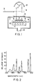
- Fig.1 shows an apparatus of treating photoresist for explaining one embodiment of a method of treating a photoresist image according to this invention.
- Fig.2 shows radiation spectra of a high pressure mercury vapor lamp employed to execute the method of treating a photoresist image according to this invention.
- Fig.3 shows a semiconductor wafer, on which the developed positive photoresist image is applied.
- Fig.4 shows charts of the intensity of ultraviolet irradiation against exposure time.
- a chamber 7 has a radiation window 8 formed of fused quartz glass at the top and an exhaust hole 12 at the bottom.
- the exhaust hole 12 is connected to a vacuum pump, not shown, which reduces the pressure of gas such as air in the chamber 7.
- a pattern of a photoresist 4 is formed on a semiconductor wafer 5, which is placed on a support 6.
- the support 6 is heated by a heater 10 connected with power supply through a heater lead wire 9, or cooled down by cooling water to flow through a cooling conduit 11.
- the temperature of the semiconductor wafer 5 is controlled by these heating and cooling mechanisms.
- Ultraviolet irradiation source arranged on the upper part of the radiation window 8 is composed of a high pressure mercury vapor lamp 1, a concave mirror 2 and a shutter 3 which can be opened and closed, etc..
- the pressure of gas in a chamber 7 is reduced to approximately 1 ⁇ 10 ⁇ 1torr.
- a figure of an electric circuit for energizing the high pressure mercury vapor lamp 1 is omitted.
- the intensity of ultraviolet radiation from a lamp is altered by controlling the electric power generated from said circuit.
- the electric circuit for lighting the high pressure mercury vapor lamp 1, publicly known or publicly used technique such as being disclosed in published documents, is available.
- Fig.2 shows the radiation spectrum of the high pressure mercury vapor lamp.
- Fig.4 shows three examples of charts of the intensity of ultraviolet irradiation which increases little by little or in steps by changing the electric power of the electric circuit for lighting the high pressure mercury vapor lamp.
- This figure is an orthogonal coordinate system with relative intensity of ultraviolet irradiation as vertical axis and exposure time as lateral axis.
- fig.4(a), 4(b), 4(c) show changes of the intensity of ultraviolet irradiation, which increases little by little for all exposure time, increases little by little for intermediate exposure time and steps up in steps, respectively.
- the following is a ore concrete description as to figure 4(c).
- a positive type photoresist image which was formed on a wafer by using novolak resin was applied to the radiant light having a wavelength below 350nm.
- the intensity of this irradiated light was 20 to 50mW/cm2 in the wavelength region below 320nm for 5 seconds from the beginning of exposure process, and 500mW/cm2 for 10 seconds thereafter.
- deformation of the photoresist pattern, formation of bubbles and deformation of the photoresist film were not caused, and effective treatment of the photoresist was enabled.
- the intensity of the irradiated light was 500mW/cm2 for 5 seconds from the beginning of the exposure, formation of bubbles, deformation of the photoresist film, etc. occurred in parts.
- irradiation intensity is kept at 20 to 50mW/cm2 in order to depress the formation of bubbles for this reason, it takes 60 to 90 seconds to treat the developed positive photoresist on a semiconductor wafer.
- exposure time for the ultraviolet radiation under a lower atmospheric pressure is decreased by about 1/4 to 1/6 times in comparison with that under 1 atmospheric pressure.
- the intensity of the light irradiated on the photoresist image placed under lower pressure is controlled by changing the intensity of the light radiated from the high pressure mercury vapor lamp.
- Another means of controlling the intensity of the light irradiated onto the photoresist can be employed instead of power control.
- means of controlling the intensity of the light irradiated onto the photoresist by employing a light source having means of decreasing ultraviolet irradiation such as' filter prepared between high pressure mercury vapor lamp and wafer may be used as well.
Claims (1)
- Verfahren zur Erhöhung der Wärmebeständigkeit eines entwickelten Positiv-Fotolackbildes (4) auf einem Halbleiter-Wafer (5), das folgende Schritte aufweist:
Positionieren des Halbleiter-Wafers (5) auf eine Auflage (6) in einer mit Gas eines niedrigeren Druckes als atmosphärischer Druck gefüllten Kammer (7),
Bestrahlen des entwickelten Positiv-Fotolackbildes mit ultraviolettem Licht von zu Beginn der Bestrahlung niedriger Intensität,
und dann Bestrahlen des entwickelten Positiv-Fotolackbildes mit ultraviolettem Licht, dessen Intensität nach und nach oder in Stufen ansteigt,
worin die Intensität der ultravioletten Strahlung gesteuert wird
durch Verändern der elektrischen Leistung des elektrischen Stromkreises zum Betreiben der Quelle ultravioletten Lichts (1),
oder durch Benutzen eines Filters zwischen der Quelle ultravioletten Lichts und dem Wafer.
Applications Claiming Priority (2)
| Application Number | Priority Date | Filing Date | Title |
|---|---|---|---|
| JP67887/87 | 1987-03-24 | ||
| JP62067887A JPH0740546B2 (ja) | 1987-03-24 | 1987-03-24 | レジスト処理方法 |
Publications (3)
| Publication Number | Publication Date |
|---|---|
| EP0283665A2 EP0283665A2 (de) | 1988-09-28 |
| EP0283665A3 EP0283665A3 (en) | 1989-01-18 |
| EP0283665B1 true EP0283665B1 (de) | 1992-04-08 |
Family
ID=13357853
Family Applications (1)
| Application Number | Title | Priority Date | Filing Date |
|---|---|---|---|
| EP88101170A Expired EP0283665B1 (de) | 1987-03-24 | 1988-01-27 | Verfahren zur Behandlung von Photolacken |
Country Status (4)
| Country | Link |
|---|---|
| US (1) | US4868095A (de) |
| EP (1) | EP0283665B1 (de) |
| JP (1) | JPH0740546B2 (de) |
| DE (1) | DE3869814D1 (de) |
Families Citing this family (4)
| Publication number | Priority date | Publication date | Assignee | Title |
|---|---|---|---|---|
| US5204224A (en) * | 1988-09-26 | 1993-04-20 | Ushio Denki | Method of exposing a peripheral part of a wafer |
| US6183937B1 (en) * | 1998-05-06 | 2001-02-06 | Taiwan Semiconductor Manufacturing Company | Post photodevelopment isotropic radiation treatment method for forming patterned photoresist layer with attenuated linewidth |
| KR20130120586A (ko) * | 2012-04-26 | 2013-11-05 | 삼성전자주식회사 | 패턴 형성 방법 |
| US8986562B2 (en) | 2013-08-07 | 2015-03-24 | Ultratech, Inc. | Methods of laser processing photoresist in a gaseous environment |
Family Cites Families (6)
| Publication number | Priority date | Publication date | Assignee | Title |
|---|---|---|---|---|
| JPS57149733A (en) * | 1981-03-11 | 1982-09-16 | Hitachi Ltd | Dry etching method |
| JPS58142525A (ja) * | 1982-02-18 | 1983-08-24 | Nec Corp | 露光方法 |
| JPS6129124A (ja) * | 1984-07-20 | 1986-02-10 | Ushio Inc | 半導体ウエハ−の処理方法 |
| JPS6155923A (ja) * | 1984-08-28 | 1986-03-20 | Toshiba Corp | レジスト処理方法 |
| JPS63260028A (ja) * | 1986-11-19 | 1988-10-27 | Tokyo Ohka Kogyo Co Ltd | ホトレジストの熱安定化装置 |
| EP0282703B1 (de) * | 1987-03-20 | 1991-01-16 | Ushio Denki | Behandlungsverfahren für Photolacke |
-
1987
- 1987-03-24 JP JP62067887A patent/JPH0740546B2/ja not_active Expired - Lifetime
-
1988
- 1988-01-27 EP EP88101170A patent/EP0283665B1/de not_active Expired
- 1988-01-27 DE DE8888101170T patent/DE3869814D1/de not_active Expired - Lifetime
- 1988-01-28 US US07/149,308 patent/US4868095A/en not_active Expired - Lifetime
Also Published As
| Publication number | Publication date |
|---|---|
| DE3869814D1 (de) | 1992-05-14 |
| EP0283665A3 (en) | 1989-01-18 |
| EP0283665A2 (de) | 1988-09-28 |
| US4868095A (en) | 1989-09-19 |
| JPS63234526A (ja) | 1988-09-29 |
| JPH0740546B2 (ja) | 1995-05-01 |
Similar Documents
| Publication | Publication Date | Title |
|---|---|---|
| JPH0527107B2 (de) | ||
| JPS63260028A (ja) | ホトレジストの熱安定化装置 | |
| EP0283666B1 (de) | Verfahren zur Behandlung von Photolacken | |
| EP0283665B1 (de) | Verfahren zur Behandlung von Photolacken | |
| EP0237631B1 (de) | Photolack-Verarbeitungsverfahren | |
| EP0233333B1 (de) | Photolack-Behandlungsverfahren | |
| EP0282703B1 (de) | Behandlungsverfahren für Photolacke | |
| EP0236559B1 (de) | Verfahren und Vorrichtung für Photolackverarbeitung | |
| EP0283667B1 (de) | Verfahren und Vorrichtung zur Behandlung von Photolacken | |
| EP0283668A2 (de) | Verfahren und Vorrichtung zur Behandlung von Photolacken | |
| JPS5936257B2 (ja) | レジスト材料の剥離方法 | |
| EP0239669B1 (de) | Verfahren und Vorrichtung für Photolackverarbeitung | |
| EP0282704A2 (de) | Verfahren zur Behandlung von Photorisisten | |
| JP2632796B2 (ja) | レジスト処理方法 | |
| JPH0812840B2 (ja) | レジスト処理方法 | |
| JPH0812841B2 (ja) | レジスト処理方法 | |
| JPH07307274A (ja) | 半導体装置の製造装置 | |
| JPS62101027A (ja) | レジスト処理方法 | |
| JPH0231857B2 (de) | ||
| JPS62296212A (ja) | 半導体ウエハ用の処理台温度制御方法 | |
| JP2692124B2 (ja) | レジスト処理方法 | |
| JPS6376332A (ja) | 半導体装置の製造方法 | |
| JPS62111424A (ja) | レジスト処理方法 | |
| JPH06291028A (ja) | レジスト硬化方法 | |
| JPH04225217A (ja) | レジスト処理方法 |
Legal Events
| Date | Code | Title | Description |
|---|---|---|---|
| PUAI | Public reference made under article 153(3) epc to a published international application that has entered the european phase |
Free format text: ORIGINAL CODE: 0009012 |
|
| AK | Designated contracting states |
Kind code of ref document: A2 Designated state(s): DE GB NL |
|
| PUAL | Search report despatched |
Free format text: ORIGINAL CODE: 0009013 |
|
| AK | Designated contracting states |
Kind code of ref document: A3 Designated state(s): DE GB NL |
|
| 17P | Request for examination filed |
Effective date: 19890421 |
|
| 17Q | First examination report despatched |
Effective date: 19890922 |
|
| GRAA | (expected) grant |
Free format text: ORIGINAL CODE: 0009210 |
|
| AK | Designated contracting states |
Kind code of ref document: B1 Designated state(s): DE GB NL |
|
| REF | Corresponds to: |
Ref document number: 3869814 Country of ref document: DE Date of ref document: 19920514 |
|
| PLBE | No opposition filed within time limit |
Free format text: ORIGINAL CODE: 0009261 |
|
| STAA | Information on the status of an ep patent application or granted ep patent |
Free format text: STATUS: NO OPPOSITION FILED WITHIN TIME LIMIT |
|
| 26N | No opposition filed | ||
| REG | Reference to a national code |
Ref country code: GB Ref legal event code: IF02 |
|
| PGFP | Annual fee paid to national office [announced via postgrant information from national office to epo] |
Ref country code: NL Payment date: 20070117 Year of fee payment: 20 |
|
| PGFP | Annual fee paid to national office [announced via postgrant information from national office to epo] |
Ref country code: GB Payment date: 20070123 Year of fee payment: 20 |
|
| PGFP | Annual fee paid to national office [announced via postgrant information from national office to epo] |
Ref country code: DE Payment date: 20070329 Year of fee payment: 20 |
|
| REG | Reference to a national code |
Ref country code: GB Ref legal event code: PE20 |
|
| NLV7 | Nl: ceased due to reaching the maximum lifetime of a patent |
Effective date: 20080127 |
|
| PG25 | Lapsed in a contracting state [announced via postgrant information from national office to epo] |
Ref country code: NL Free format text: LAPSE BECAUSE OF EXPIRATION OF PROTECTION Effective date: 20080127 |
|
| PG25 | Lapsed in a contracting state [announced via postgrant information from national office to epo] |
Ref country code: GB Free format text: LAPSE BECAUSE OF EXPIRATION OF PROTECTION Effective date: 20080126 |