EP0283668A2 - Verfahren und Vorrichtung zur Behandlung von Photolacken - Google Patents
Verfahren und Vorrichtung zur Behandlung von Photolacken Download PDFInfo
- Publication number
- EP0283668A2 EP0283668A2 EP88101173A EP88101173A EP0283668A2 EP 0283668 A2 EP0283668 A2 EP 0283668A2 EP 88101173 A EP88101173 A EP 88101173A EP 88101173 A EP88101173 A EP 88101173A EP 0283668 A2 EP0283668 A2 EP 0283668A2
- Authority
- EP
- European Patent Office
- Prior art keywords
- positive photoresist
- lamp
- photoresist image
- photoresist
- image
- Prior art date
- Legal status (The legal status is an assumption and is not a legal conclusion. Google has not performed a legal analysis and makes no representation as to the accuracy of the status listed.)
- Granted
Links
Images

Classifications
-
- G—PHYSICS
- G03—PHOTOGRAPHY; CINEMATOGRAPHY; ANALOGOUS TECHNIQUES USING WAVES OTHER THAN OPTICAL WAVES; ELECTROGRAPHY; HOLOGRAPHY
- G03F—PHOTOMECHANICAL PRODUCTION OF TEXTURED OR PATTERNED SURFACES, e.g. FOR PRINTING, FOR PROCESSING OF SEMICONDUCTOR DEVICES; MATERIALS THEREFOR; ORIGINALS THEREFOR; APPARATUS SPECIALLY ADAPTED THEREFOR
- G03F7/00—Photomechanical, e.g. photolithographic, production of textured or patterned surfaces, e.g. printing surfaces; Materials therefor, e.g. comprising photoresists; Apparatus specially adapted therefor
- G03F7/20—Exposure; Apparatus therefor
- G03F7/2022—Multi-step exposure, e.g. hybrid; backside exposure; blanket exposure, e.g. for image reversal; edge exposure, e.g. for edge bead removal; corrective exposure
- G03F7/2024—Multi-step exposure, e.g. hybrid; backside exposure; blanket exposure, e.g. for image reversal; edge exposure, e.g. for edge bead removal; corrective exposure of the already developed image
Definitions
- This invention relates to a method and an apparatus of treating positive photoresist materials applied on semiconductor wafer and, more particularly, to a method and an apparatus of treating the developed positive photoresist image on a semiconductor wafer placed in a chamber by employing ultraviolet irradiation.
- the baking process is employed between a process of "forming a photoresist pattern, exposing and developing the photoresist” and a process of "executing ion implantation, plasma-etching, etc.”, and said process is composed of a heating process executed for improving the adhesiveness of the photoresist to a semiconductor wafer and heat-resistance of said photoresist. While a reference of H. Hiraoka and J. Pacansky: J. Vac. Sci. Tech. 19(1981), and U.S.
- Application No.923,553 have disclosed a method in which ultraviolet rays are applied to the developed positive photoresist image after or during the baking process after "development process" so as to enhance the heat-resistance and plasma-resistance of the positive photoresist through the baking process in a shorter time.
- a light having a high ultraviolet intensity such as a radiant light from a discharge lamp such as high pressure mercury vapor lamp having a high ultraviolet radiation efficiency
- gas is generated from the photoresist, and this gas causes the formation of bubbles, deformation of a photoresist pattern and breakdown of a photoresist film, such as exfoliation, rupture or roughening hereof, thus causing imperfections of a semiconductor device.
- this gas is caused by a rapid photochemical reaction of the light sensitive radicals of the photoresist materials, for instance, by the photochemical reaction of HMDS(hexamethyldisilazine), which is applied to a wafer as a preliminary treatment for the good coating of the photoresist onto a wafer or of an anti-reflection coating on the photoresist film, by the photochemical reaction of an additive materials to the photoresist materials such as dyestuff, by the photochemical reaction of a solvent remaining in the photoresist film.
- HMDS(hexamethyldisilazine) which is applied to a wafer as a preliminary treatment for the good coating of the photoresist onto a wafer or of an anti-reflection coating on the photoresist film
- the photochemical reaction of an additive materials to the photoresist materials such as dyestuff
- An object of this invention is to provide a method and an apparatus enabling the high-speed and effective treatment of the developed positive photoresist image prepared on a semiconductor wafer placed in a chamber employing ultraviolet irradiation by preventing the deformation of the photoresist image which is caused by the light radiated from the discharge lamp such as high pressure mercury vapor lamp.
- ultraviolet rays are applied to the developed positive photoresist image, using a means to intercept or reduce selectively all or any part of the wavelengths in the spectral response region of the positive photoresist out of radiant lights obtained from the discharge lamp such as high pressure mercury vapor lamp.
- the light applied to the photoresist image still contains a strong ultraviolet component being effective for improving the heat-resistance and plasma-etching-resistance of the positive photoresist even when the wavelengths in the spectral response region of the positive photoresist are intercepted or re cuted.
- an inventive method enabling the high-speed and effective treatment of the developed positive photoresist image on a semiconductor wafer is accomplished.
- Fig.1 shows an embodiment of an apparatus of treating a photoresist for explaining one embodiment of a method for treatment of developed positive photoresists prepared on a semiconductor wafer according to this invention.
- a chamber 7 has a radiation window 8 formed of quartz glass at the top and an exhaust hole 14 at the bot tom.
- the exhaust hole 14 is connected to a vacuum pump, not shown, which reduces the pressure of gas in the chamber 7 to approximately 1 ⁇ 10 ⁇ 1torr.
- a pattern of a developed positive photoresist image 4 is formed on a semiconductor wafer 5, which is placed on a support 6.
- the support 6 is heated by a heater 10 connected with power supply through a heater lead wire 9, or cooled down by cooling water to flow through a cooling conduit 11.
- the temperature of the semiconductor wafer 5 is controlled by these heating and cooling mechanisms.
- Ultraviolet radiation source arranged on the upper part of the radiation window 8 is composed of a high pressure mercury vapor lamp 1, a concave mirror 2, a filter 3, etc..
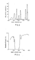
- Fig.3 shows one example of the radiation spectrum of the high pressure mercury vapor lamp 1 employed in this embodiment.
- the filter 3 intercepting or reducing a light in the wavelength region of 300nm to 500nm, that is, a wavelength region including the wavelengths in the spectral response region of the positive photoresist, is employed herein, and thereby the treatment of the positive photoresist on a wafer employing ultraviolet irradiation and temperature control in a chamber filled with gas of lower than 1 atmospheric pressure can be performed effectively.
- a filter prepared by forming a multilayer evaporation film on a glass plate for obtaining the characteristic of intercepting or reducing the light in the wavelength region of 300nm to 500nm.
- the glass plate preferable for this filter is of the fused silica, which is showing a large transmittance of ultraviolet rays of a wavelength 300nm or below which are effective for the improvement in the heat-resistance and plasma-etching-resistance of the positive photoresist.
- the radiant light from the high pressure mercury vapor lamp is applied to a sample which was prepared by using the novolak type positive photoresist which is 1.5 ⁇ m or more of thickness, and HMDS as an agent which is applied to a wafer as a preliminary treatment for the application of the said photoresist.
- the photoresist image is treated by placing in gas of lower pressure than 1 atmospheric pressure, the time for treating photoresist image is shortened which is 1/5 times in comparison with the time of treating same in the air of 760 torr.
- Fig.2 shows another embodiment in which a mirror is employed as a means to intercept or reduce the radiant light in a wavelength region of 300nm to 500nm.
- the mirror 12 employed herein has a characteristic of reflecting a radiant light in a wavelength region below 300nm and not reflecting the radiant light of 300nm to 500nm.
- a mirror formed of a multilayer film evaporated on glass is suitable also for the mirror having the above-mentioned characteristic.
- a high pressure mercury vapor lamp is used to get the high intensity radiation of ultraviolet lights.
- Another lamps can be used instead of this lamp.
- a metal-halide discharge lamp containing a filling comprised of a very small quantity of metal other than mercury in the form of a halide, for instance, may be used as well on condition that the lamp radiates ultraviolet rays of a ultraviolet wavelength region, and further mercury-rare gas discharge lamp containing a filling comprised of mercury and rare gas as the source radiating a ultraviolet wavelength region may also be employed.
- the filter or the mirror is employed separately as a means to intercept or reduce the light having the wavelengths in the spectral response region of the positive photoresist. It is a matter of course that a various combination of different filters and mirrors may be employed.
Landscapes
- Physics & Mathematics (AREA)
- General Physics & Mathematics (AREA)
- Exposure Of Semiconductors, Excluding Electron Or Ion Beam Exposure (AREA)
- Exposure And Positioning Against Photoresist Photosensitive Materials (AREA)
- Photosensitive Polymer And Photoresist Processing (AREA)
- Drying Of Semiconductors (AREA)
Applications Claiming Priority (2)
| Application Number | Priority Date | Filing Date | Title |
|---|---|---|---|
| JP62067888A JPS63234527A (ja) | 1987-03-24 | 1987-03-24 | レジスト処理方法 |
| JP67888/87 | 1987-03-24 |
Publications (3)
| Publication Number | Publication Date |
|---|---|
| EP0283668A2 true EP0283668A2 (de) | 1988-09-28 |
| EP0283668A3 EP0283668A3 (en) | 1989-01-18 |
| EP0283668B1 EP0283668B1 (de) | 1991-03-13 |
Family
ID=13357883
Family Applications (1)
| Application Number | Title | Priority Date | Filing Date |
|---|---|---|---|
| EP88101173A Expired EP0283668B1 (de) | 1987-03-24 | 1988-01-27 | Verfahren und Vorrichtung zur Behandlung von Photolacken |
Country Status (4)
| Country | Link |
|---|---|
| US (1) | US4888271A (de) |
| EP (1) | EP0283668B1 (de) |
| JP (1) | JPS63234527A (de) |
| DE (1) | DE3861978D1 (de) |
Families Citing this family (3)
| Publication number | Priority date | Publication date | Assignee | Title |
|---|---|---|---|---|
| JPH0427113A (ja) * | 1990-04-23 | 1992-01-30 | Tadahiro Omi | レジスト処理装置、レジスト処理方法及びレジストパターン |
| US8986562B2 (en) | 2013-08-07 | 2015-03-24 | Ultratech, Inc. | Methods of laser processing photoresist in a gaseous environment |
| US9541836B2 (en) * | 2014-02-10 | 2017-01-10 | Taiwan Semiconductor Manufacturing Co., Ltd. | Method and apparatus for baking photoresist patterns |
Citations (3)
| Publication number | Priority date | Publication date | Assignee | Title |
|---|---|---|---|---|
| JPS6155923A (ja) * | 1984-08-28 | 1986-03-20 | Toshiba Corp | レジスト処理方法 |
| EP0195106A1 (de) * | 1985-03-22 | 1986-09-24 | Ibm Deutschland Gmbh | Herstellung einer Abhebemaske und ihre Anwendung |
| EP0239669A2 (de) * | 1986-03-31 | 1987-10-07 | Ushio Denki Kabushiki Kaisha | Verfahren und Vorrichtung für Photolackverarbeitung |
Family Cites Families (3)
| Publication number | Priority date | Publication date | Assignee | Title |
|---|---|---|---|---|
| JPS58218126A (ja) * | 1982-06-14 | 1983-12-19 | Nippon Telegr & Teleph Corp <Ntt> | リフトオフ加工用真空蒸着装置およびその使用方法 |
| US4548688A (en) * | 1983-05-23 | 1985-10-22 | Fusion Semiconductor Systems | Hardening of photoresist |
| JPS63260028A (ja) * | 1986-11-19 | 1988-10-27 | Tokyo Ohka Kogyo Co Ltd | ホトレジストの熱安定化装置 |
-
1987
- 1987-03-24 JP JP62067888A patent/JPS63234527A/ja active Pending
-
1988
- 1988-01-22 US US07/146,926 patent/US4888271A/en not_active Expired - Lifetime
- 1988-01-27 DE DE8888101173T patent/DE3861978D1/de not_active Expired - Lifetime
- 1988-01-27 EP EP88101173A patent/EP0283668B1/de not_active Expired
Patent Citations (3)
| Publication number | Priority date | Publication date | Assignee | Title |
|---|---|---|---|---|
| JPS6155923A (ja) * | 1984-08-28 | 1986-03-20 | Toshiba Corp | レジスト処理方法 |
| EP0195106A1 (de) * | 1985-03-22 | 1986-09-24 | Ibm Deutschland Gmbh | Herstellung einer Abhebemaske und ihre Anwendung |
| EP0239669A2 (de) * | 1986-03-31 | 1987-10-07 | Ushio Denki Kabushiki Kaisha | Verfahren und Vorrichtung für Photolackverarbeitung |
Non-Patent Citations (5)
| Title |
|---|
| JOURNAL OF THE ELECTROCHEMICAL SOCIETY, vol. 128, no. 12, December 1981, pages 2645-2647, Manchester, N.H., US; H. HIRAOKA et al.: "High temperature flow resistance of micron sized images in AZ resists" * |
| JOURNAL OF THE ELECTROCHEMICAL SOCIETY, vol. 129, no. 6, June 1982, pages 1379-1381, Manchester, N.H., US; R. ALLEN et al.: "Deep U.V. hardening of positive photoresist patterns" * |
| PATENT ABSTRACTS OF JAPAN, vol. 10, no. 217 (E-423)(2273), 29th July 1986; & JP-A-61 055 923 (TOSHIBA CORP.) 20-03-1986 * |
| SOLID STATE TECHNOLOGY, vol. 25, no. 2, February 1982, pages 124-127, Washington, New York, US; J. BACHUR: "Deep UV exposure technology" * |
| SOLID STATE TECHNOLOGY, vol. 27, no. 7, July 1984, pages 45-46, Port Washington, N.Y., US; "Photoresist stabilization system" * |
Also Published As
| Publication number | Publication date |
|---|---|
| US4888271A (en) | 1989-12-19 |
| EP0283668A3 (en) | 1989-01-18 |
| DE3861978D1 (de) | 1991-04-18 |
| EP0283668B1 (de) | 1991-03-13 |
| JPS63234527A (ja) | 1988-09-29 |
Similar Documents
| Publication | Publication Date | Title |
|---|---|---|
| US4841342A (en) | Apparatus for treating photoresists | |
| EP0283666A2 (de) | Verfahren zur Behandlung von Photolacken | |
| US4900938A (en) | Method of treating photoresists | |
| EP0283668A2 (de) | Verfahren und Vorrichtung zur Behandlung von Photolacken | |
| US4882263A (en) | Method of treating photoresists | |
| EP0239669B1 (de) | Verfahren und Vorrichtung für Photolackverarbeitung | |
| US4868095A (en) | Method of treating photoresists | |
| EP0233333B1 (de) | Photolack-Behandlungsverfahren | |
| JP2978620B2 (ja) | レジスト膜のアッシング装置 | |
| JP2632796B2 (ja) | レジスト処理方法 | |
| EP0282704A2 (de) | Verfahren zur Behandlung von Photorisisten | |
| JPH0812840B2 (ja) | レジスト処理方法 | |
| JPH0812841B2 (ja) | レジスト処理方法 | |
| JPH07307274A (ja) | 半導体装置の製造装置 | |
| JPH04307734A (ja) | アッシング装置 | |
| JPS6114724A (ja) | 半導体ウエハ−への紫外線照射方法 | |
| JPS62101027A (ja) | レジスト処理方法 | |
| JPH0763048B2 (ja) | 半導体装置製造用レジスト硬化装置 | |
| JPH03208340A (ja) | 光励起ドライエッチング装置 | |
| JPS62111424A (ja) | レジスト処理方法 | |
| JPS63232331A (ja) | レジスト処理方法 | |
| JPS63261834A (ja) | レジスト硬化方法 | |
| JPS62111425A (ja) | レジスト処理方法 | |
| JPH04307726A (ja) | アッシング装置 | |
| JPS61154038A (ja) | ドライアツシング装置 |
Legal Events
| Date | Code | Title | Description |
|---|---|---|---|
| PUAI | Public reference made under article 153(3) epc to a published international application that has entered the european phase |
Free format text: ORIGINAL CODE: 0009012 |
|
| AK | Designated contracting states |
Kind code of ref document: A2 Designated state(s): DE GB NL |
|
| PUAL | Search report despatched |
Free format text: ORIGINAL CODE: 0009013 |
|
| AK | Designated contracting states |
Kind code of ref document: A3 Designated state(s): DE GB NL |
|
| 17P | Request for examination filed |
Effective date: 19890421 |
|
| 17Q | First examination report despatched |
Effective date: 19890922 |
|
| GRAA | (expected) grant |
Free format text: ORIGINAL CODE: 0009210 |
|
| AK | Designated contracting states |
Kind code of ref document: B1 Designated state(s): DE GB NL |
|
| REF | Corresponds to: |
Ref document number: 3861978 Country of ref document: DE Date of ref document: 19910418 |
|
| PLBE | No opposition filed within time limit |
Free format text: ORIGINAL CODE: 0009261 |
|
| STAA | Information on the status of an ep patent application or granted ep patent |
Free format text: STATUS: NO OPPOSITION FILED WITHIN TIME LIMIT |
|
| 26N | No opposition filed | ||
| REG | Reference to a national code |
Ref country code: GB Ref legal event code: IF02 |
|
| PGFP | Annual fee paid to national office [announced via postgrant information from national office to epo] |
Ref country code: NL Payment date: 20070117 Year of fee payment: 20 |
|
| PGFP | Annual fee paid to national office [announced via postgrant information from national office to epo] |
Ref country code: GB Payment date: 20070123 Year of fee payment: 20 |
|
| PGFP | Annual fee paid to national office [announced via postgrant information from national office to epo] |
Ref country code: DE Payment date: 20070329 Year of fee payment: 20 |
|
| REG | Reference to a national code |
Ref country code: GB Ref legal event code: PE20 |
|
| NLV7 | Nl: ceased due to reaching the maximum lifetime of a patent |
Effective date: 20080127 |
|
| PG25 | Lapsed in a contracting state [announced via postgrant information from national office to epo] |
Ref country code: NL Free format text: LAPSE BECAUSE OF EXPIRATION OF PROTECTION Effective date: 20080127 |
|
| PG25 | Lapsed in a contracting state [announced via postgrant information from national office to epo] |
Ref country code: GB Free format text: LAPSE BECAUSE OF EXPIRATION OF PROTECTION Effective date: 20080126 |