EP0278526A2 - Contrôleur d'affichage graphique à fonction de limitation - Google Patents
Contrôleur d'affichage graphique à fonction de limitation Download PDFInfo
- Publication number
- EP0278526A2 EP0278526A2 EP88102202A EP88102202A EP0278526A2 EP 0278526 A2 EP0278526 A2 EP 0278526A2 EP 88102202 A EP88102202 A EP 88102202A EP 88102202 A EP88102202 A EP 88102202A EP 0278526 A2 EP0278526 A2 EP 0278526A2
- Authority
- EP
- European Patent Office
- Prior art keywords
- word
- data
- bit
- area
- coordinate data
- Prior art date
- Legal status (The legal status is an assumption and is not a legal conclusion. Google has not performed a legal analysis and makes no representation as to the accuracy of the status listed.)
- Granted
Links
Images


Classifications
-
- G—PHYSICS
- G09—EDUCATION; CRYPTOGRAPHY; DISPLAY; ADVERTISING; SEALS
- G09G—ARRANGEMENTS OR CIRCUITS FOR CONTROL OF INDICATING DEVICES USING STATIC MEANS TO PRESENT VARIABLE INFORMATION
- G09G5/00—Control arrangements or circuits for visual indicators common to cathode-ray tube indicators and other visual indicators
- G09G5/36—Control arrangements or circuits for visual indicators common to cathode-ray tube indicators and other visual indicators characterised by the display of a graphic pattern, e.g. using an all-points-addressable [APA] memory
- G09G5/39—Control of the bit-mapped memory
- G09G5/393—Arrangements for updating the contents of the bit-mapped memory
-
- G—PHYSICS
- G06—COMPUTING; CALCULATING OR COUNTING
- G06T—IMAGE DATA PROCESSING OR GENERATION, IN GENERAL
- G06T15/00—3D [Three Dimensional] image rendering
- G06T15/10—Geometric effects
- G06T15/30—Clipping
Definitions
- the present invention relates to a graphics display controller for managing a display memory and drawing figures on a screen of a raster-scan display and, more particularly, to such a controller having a clipping function for clipping or limiting a drawing area of figures on a display screen.
- a clipping function is used to allow figures to be drawn only into an inside (or outside) area of a rectangle which has a diagonal line defined by two coordinate data on a display screen. This rectangle is called hereinafter "clipping rectangle".
- clipping rectangle When figure data of a first area are transferred, by use of the clipping function, to a second area which has one portion contained in a drawing-enable area defined by the clipping rectangle, only data of that portion of the second area should be replaced by the figure data of the first area.
- the coordinate data of every dot is compared with the above-mentioned two coordinate data to detect the portion of the second area overlapping the drawing-enable area defined by the clipping rectangle and the data of the portion of the second area are replaced one-bit by one-bit by the figure data of the first area. For this reason, a considerably long processing time is required.
- an object of the present invention is to provide a graphics display controller executing a clipping function at a high speed.
- Another object of the present invention is to provide a graphics display controller which transfers at a high speed figure data to a drawing-enable area defined by a clipping rectnagle without a complicated circuit construction.
- a graphics display controller having a function of transferring figure data of a source to a destination area including a portion contained in a drawing-enable area defined by a clipping rectangle having a diagonal line defined by first and second coordinate data, comprises comparing means for comparing coordinate data of each word of the destination area with the first and second coordinate data to detect that the coordinate data of each word is within or out of the drawing-enable area or is the same as a boundary of the drawing-enable area, first generating means responsive to comparison result of the comparing means for generating first information designating bit or bits whose data are allowed to be rewritten in each word of the destination area, second generating means responsive to a position of each word of the destination area for generating second information designating bit or bits whose data are allowed to be rewritten in each word of the destination area, and means for writing the figure data into the bit or bits which are designated by both of the first and second information in each word of the destination area.
- the coordinate data of each word, not each bit, of the destination area is compared with the first and second coordinate data which are used for defining the clipping rectangle, and the data of each word, not each bit, of the destination area are controlled to be replaced or not replaced by the figure data.
- a processing time is thereby shortened.
- the first information representative of clipping mask information and the second information representative of drawing mask information are generated independently of each other.
- the second information designates similarly all the bits whose data are allowed to be rewritten, the data of all bits of this word is rewritten or replaced by the figure data to be drawn.
- the second information designates several bits, not all bits, whose data are to be written, only the data thereof are rewritten by the figure data.
- the comparison result represents that the coordinate data of the word of the destination area is out of the drawing-enable area
- the first information designates no bit whose data is allowed to be rewritten, because this word is outside the drawing-enable area. The data of all the bits of this word are thereby not rewritten irrespective of the second mask information.
- the first information designates a plurality of bits, but not all bits, which are inside the drawing-enable area.
- one or more bits in the word which are designated by both of the first and second information are rewritten by the figure data.
- the figure data only the data of the portion of the destination area, which is contained in the drawing-enable area defined by the clipping rectangle, are rewritten by the figure data to be drawn.
- a graphics display controller 1 receives instructions from a host processor 2 and manages a display memory 3.
- the controller 1 further draws various figures on a display screen of a cathode-ray tube (CRT) 4 by use of data stored in the display memory 3.
- the CRT 4 is supplied with synchronizing signals from the controller 1.
- the graphics display controller 1 includes a sequencer 10 generating various timing signals and data for executing the instructions from the host processor 2.
- the controller 1 further includes a clipping performing section 5 in accordance with the present invention. Before the description is made on a construction and an operation of the clipping performing section 5, a clipping function with respect to figure data transmission operation will be described below with reference to Fig. 2.
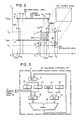
- Fig. 2 shows a display screen of the CRT 4, and a horizontal direction of the display screen is defined as an X-axis and a vertical direction thereof is defined as a Y-axis.
- Each of dots of the display screen corresponds to each of bits of the display memory 3. Therefore, the diagram shown in Fig. 2 can be regarded as a memory map of the display memory 3 and each bit of the display memory 3 has individual coordinate data on the display screen.
- the display memory 3 consists of a plurality of words, each of which is constructed by sixteen bits. The coordinate data of each word or each bit also represents address data thereof.
- each of characters W1 to W10 represents each of boundaries of the words arranged in the direction of the X-axis.
- a clipping rectangle 200 is defined as a rectangle having a diagonal line, one end of which positions at a first clipping coordinate (X min , Y min ) and the other end of which positions at a second clipping coordinate (X max , Y max ).
- An inside area 201 of the clipping rectangle 200 is employed as a drawing-enable area. That is, figures are allowed to be drawn only within this drawing-enable area 201. If desired, an outside area of the clipping rectangle 200 can be employed as a drawing-enable area. As shown in Fig.
- a source area 202 includes figure data to be transferred, and this figure data is transferred to a destination area 203in response to a bit-block-transfer instruction supplied from the host processor 2.
- This destination area 203 is a rectangular area having a diagonal line defined by two coordinates represented by (Xs, Ys) and (Xe, Ye) and has the same size as the source area 202.
- the destination area 203 has one portion 203-1 denoted by oblique lines and included in the drawing-enable area 201 defined by the clipping rectangle 200.
- the left side of the destination area 203 is apart from the word boundary W4 by the number of bits represented as third offset data "DS" and the right side thereof is apart from the word boundary W10by the number of bits represented as fourth offset data "DE". Since only the portion 203-1 of the destination area 203 is included in the drawing-enable area 201, all the figure data of the source area 202 are not transferred to the destination area 203, but only the data of the portion 203-1 of the destination area 203 are rewritten or replaced by the figure data of the corresponding portion of the source area 202.
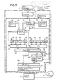
- the clipping performing section 5 of the graphics display controller 1 shown in Fig. 1 executes a data processing operation in word units and generates clipping mask information and drawing mask information independently of each other.
- the clipping mask information is generated by a coordinate arithmetic circuit 20, a clipping comparator 30, a selection controller 50, registers 70, 80, 90, 110, 120 and 130, multiplexers 140 and 160, a mask ROM (read only memory) 160, and a clipping mask register 170.
- the coordinate arithmetic circuit 20 calculates X-coordinate data and Y-coordinate data of a starting bit (LSB) of each word, not those of each bit, in the destination area 203.
- the construction of the circuit 20 is shown in Fig. 3.
- the sequencer 10 writes a value of the X-coordinate data Xs ⁇ into a register 22 and a value of the Y-coordinate data Ys into a register 23 via a multiplexer 201, respectively.
- the X-coordinate data Xs ⁇ represents the starting bit of the word that has the bit designated by the X-coordinate data Xs.
- the coordinate data Xs ⁇ is obtained by changing less significant four bits of the coordinate Xs to "0000".
- the initial X-coordinate data X's and Y-coordinate data Ys represents a point E shown in Fig. 2.
- the contents of the registers 22 and 23 are supplied to the clipping comparator 30 and further to an adder 28 via a multiplexer 26 in time-sharing.
- a multiplexer 27 selects a register 24 and transfers the content thereof to the adder 28.
- the register 24 stores a value of 16 in decimal, i.e. 10(H) in hexadecimal.
- the mark "(H)" denotes a hexadecimal representation.
- the adder 28 adds the content of the register 24 to the content of the register 22 and feeds the result back to the register 22 via the multiplexer 21.
- the multiplexer 26 selects the content of the register 23.
- the multiplexer 27 thus selects a register 25 storing a value of 1.
- the adder 28 adds the content of the register 25 to the content of the register 23 and feeds the result back to the register 23.
- the register 22 is thereafter rewritten with the initial data X s ⁇ .
- the X-coordinate data and Y-coordinate data designating the starting bit of each word contained in the destination area 203 are calculated by the coordinate arithmetic circuit 20 and then supplied to the clipping comparator 30 in order.
- the clipping comparator 30 compares the X-coordinate data X and Y-coordinate data Y supplied from the coordinate arithmetic circuit 20 with the first and second clipping coordinate data (X min , Y min ) and (X max , Y max ) to detect the word or words of the destination area 203 which are contained in the drawing-enable area 201. Since the X-coordinate data X supplied from the circuit 20 designates the starting bit of each word in the designation area 203, the first clipping X-coordinate data X min is preferably converted into a first virtual X-coordinate data X ⁇ min that designates the starting bit (LSB) of the word having the bit designated by the first clipping X-coordinate X min .
- the second clipping X-coordinate data X max is preferably converted into a second virtual X-coordinate data X ⁇ max that designates the starting bit (LSB) of the word having the bit designated by the second clipping X-coordinate data X max .
- the first and second virtual X-coordinate data X ⁇ min and X max are obtained by changing values of less significant four bits of the first and second clipping X-coordinate data X min and X max to "0000", respectively. That is, the clipping comparator 30 employs a virtual clipping rectangle defined by four points A, B, C and D shown in Fig. 2 to perform a comparing operation in word units.
- the clipping comparator 30 executes the following four arithmetic operations with respect to the X and Y coordinate data of each word of the destination area 203.
- X - Y min , Y - Y max X - X ⁇ min , X - X ⁇ max As shown in Fig. 4, the sequencer 10 writes in an initial state the first virtual X-coordinate data X ⁇ min , the second virtual X-coordinate data X ⁇ max , the first clipping Y-coordinate data Y min and the second clipping Y-coordinate data Y max into registers 33, 34, 35 and 36, respectively.
- the calculated X-coordinate and Y-coordinate data X and Y generated from the coordinate arithmetic circuit 20 are written into registers 31 and 32, respectively.
- a multiplexer 37 supplies the contents of the registers 31 and 32 to a first set of input terminals I1 of a subtracter 39 in time-sharing.
- a multiplexer 38 supplies the contents of the registers 33 and 34 to a second set of input terminals I2 of the subtracter 39 in time-sharing.
- the multiplexer 38 supplies the contents of the registers 35 and 36 to the subtracter 39 in time-sharing.
- the subtracter 39 has first and second output terminals O1 and O2.
- the first output terminal O1 takes logic "1" only when the first data DI1 supplied to the first input terminal I1 is larger than the second data DI2 supplied to the second input terminal I2, and the second output terminal O2 takes logic "1" only when the first and second data DI1 and DI2 are equal to each other.
- the clipping comparator 30 performs at first the comparing operation with respect to the Y-coordinate data and thereafter does with respect to the X-coordinate data. Thus, the clipping comparator 30 detects the word or words in the destination area 203 which are contained inside the virtual clipping rectangle defined by the points A, B, C and D shown in Fig. 2.
- the selection controller 14 receives and stores the comparison results from the clipping comparator 2 and generates selecting control signals to control the multiplexers 140 and 150.
- the controller 14 further receives detection outputs from a word detection circuit 40 which will be described later and from the clipping comparator 30 a control signal 30-1 representing that the clipping comparator 30 is performing the comparing operation.
- the controller 14 is supplied with the control signal 30-1, it does not receive the detection outputs from the circuit 40.
- the multiplexer 140 selects one of the registers 70, 80 and 90 and the multiplexer 150 selects one of the registers 110, 120 and 130 in response to the selecting control signals supplied from the controller 50.
- the clipping comparator 30 employs the virtual clipping rectangle defined by the points A, B, C and D shown in Fig. 2, if the X-coordinate data X is coincident with the first or second virtual X-coordinate data X ⁇ min or X ⁇ max , a correction is requires to obtain true clipping mask information.
- the first and second offset data LEFT and RIGHT are written into the registers 90 and 130 by the sequencer 10, respectively.
- the registers 70 and 110 stores a value of "0" and the registers 80 and 120 stores a value of "F" (i.e. "1111").
- the multiplexer 140 and 150 are controlled by the selection controller 150, as shown in the following TABLE-1.
- the output data from the multiplexers 140 and 150 i.e. eight bits data in total, are supplied to the mask ROM 160 as address information. Assuming that the number of bits represented by the first offset data "LEFT" is 5 and that represented by the second offset data "RIGHT” is 10, the mask ROM 160 generates clipping mask information consisting of sixteen bits and indicated in the following TABLE-2 in response to the address information supplied from the multiplexers 140 and 150.
- "0" of the clipping mask information represents drawing-disenable information. That is, the data of the corresponding bit of the destination area 203 must not be rewritten or replaced by the figure data of the source area 202.
- "1" of the clipping mask information represents drawing-enable information in which the data of the corresponding bit of the destination area 203 is allowed to be rewritten by the figure data of the source area 202. More specifically, a fact that the calculated Y-coordinate data Y of the word in the destination area 203 is smaller than the first clipping Y-coordinate data Y min or larger than the second clipping Y-coordinate data Y max represents that all the bits of this word lie outside the drawing-enable area 201.
- all the bits of the word of the destination area 203 are contained in the drawing-enable area 201, all the bits of the clipping mask information take the drawing-enable information (i.e., all "1").
- the word of the destination area 203 includes the left side of the drawing-enable area 201, the data from the starting bit (LSB) to the bit designated by the first offset data (i.e. the first correction data) "LEFT" are "0" (the drawing-disenable information) and the remaining bits take "1".
- the word of the destination area 203 includes the right side of the drawing-enable area 201, the data from the starting bit (LSB) to the bit designated by the second offset data (i.e., the second correction data) "RIGHT” are "1", and the remaining bits take "0".
- the word of the destination area 203 includes both of the left and right sides of the drawing-enable area 201, the data from the starting bit (LSB) to the bit designated by the first offset data “LEFT” are "0", and the data from the bit next to the bit designated by the first offset data “LEFT” to the bit designated by the second offset data “RIGHT” are "1", the remaining bits taking "0".
- the clipping mask information is generated from the mask ROM 160 in response to the relationship between the drawing-enable area 201 and the location of each word of the destination area 203. Since the mask ROM 160 is employed, various clipping mask information is generated without a complicated circuit construction.
- the output of the multiplexer 140 is supplied to the ROM 160 as more significant address information and the output of the multiplexer 150 is supplied thereto as less significant address information.
- the control signal 30-1 from the clipping comparator 30 is further supplied to the clipping mask register 170 as a store-enable signal.
- the register 170 stores the clipping mask information therein in response to the change of the signal 30-1 from the active level to the inactive level, i.e. when the clipping comparator 30 completes the coordinate data comparing operation with respect to one word in the destination area 203.
- the clipping mask information stored in the register 170 is supplied to an AND gate circuit 180 consisting of sixteen AND gates.
- the selection controller 50 receives the detection outputs of the word detection circuit 40 in place of the results from the comparator 30.
- the drawing mask information is used for defining the destination area 203 and is generated by the word detection circuit 40, the selection controller 50, registers 60, 70, 100 and 120, the multiplexers 140 and 150, and the mask ROM 160.
- the registers 80, 90, 110 and 130 are not used.
- the word detection circuit 40 delects what number of words in the destination area 203 is processed and supplies the detection outputs to the controller 50.
- the circuit 40 includes a word number register 42 in which the number of words in the horizontal direction of the destination area 203 is written in an initial state via a multiplexer 42 by the sequencer 10.
- a control signal used for controlling the multiplexer 41 so as to transfer the data from the sequencer 10 to the register 42 is supplied to a first output terminal O41 of the circuit 40. Accordingly, the output terminal O41 takes logic "1" only when the first word (i.e., the left end word) in the horizontal direction of the destination area 203 is processed.
- the content of the register 42 is supplied to one input end of a subtracter 44 having the other end supplied with a value of "1" from a register 43.
- the subtracter 44 subtracts the content of the register 43 from the content of the register 42 and feeds the result back to the register 42.
- the subtraction result of the subtracter 44 is further supplied to a zero-detector 45 which produces logic "1" to a second output terminal O42 when the result of the subtracter 44 is zero. Accordingly, the second output terminal O42 takes logic "1" when the last word (i.e., the right end word) in the horizontal direction of the destination area 203 is processed.
- both of the output terminals O41 and O42 take logic "0".
- the logic "1" from the second output terminal O42 is supplied to the sequencer 10, so that the sequencer 10 writes the number of words into the register 42 via the multiplexer 41 when the processing operation with respect to the last word in the horizontal direction of the destination area 203 is completed.
- the sequencer 10 further writes the initial X-coordinate value X's into the register 22 (see Fig. 3) of the coordinate arithmetic circuit 20.
- the selection controller 50 receives the detection outputs from the word detection circuit 40 and produces selecting control signals to the multiplexers 140 and 150 which in turn select one of the registers 60 and 70 and one of the registers 100 and 120, respectively.
- the correction using the third and fourth offset data "DS" and “DE” is required to obtain the drawing mask information.
- the third and fourth offset data "DS" and “DE” are written into the resiters 60 and 100 by the sequencer 10, respectively.
- the multiplexers 140 and 150 are controlled by the selection controller 50, as shown in the following TABLE-3.
- the outputs of the multiplexers 140 and 160 i.e. eight bits data in total, are supplied to the mask ROM 160 as address information. Assuming that a value of the third offset data "DS" is 8 and that of the fourth offset data "DE" is 4, the mask ROM generates the drawing mask information consisting of sixteen bits and indicated in the following TABLE-4.
- "0" of the drawing mask information represents the drawing-disenable information and "1" thereof represents the drawing-enable information. More specifically, when the first word in the horizontal direction of the destination area 203 is processed, this word includes the left side of the destination area 203. Accordingly, the data from the starting bit (LSB) to the bit designated by the offset data "DS" are “0", and the remaining bits take “1". The last word in the horizontal direction of the destination area 203 includes the right side of the destination area 203, and therefore the data from the starting bit (LSB) to the bit designated by the offset data "DE” are "1" and the remaining bits take "0". With respect to the intermediate words, all the bits of the drawing mask information take "1". Thus, the drawing mask information for defining the true destination area 203 is generated from the mask ROM 160 and then supplied to the AND gate circuit 180.
- the AND gate circuit 180 includes sixteen AND gates (not shown), each of which receives the associated bit data of the drawing mask information and the clipping mask information. Therefore, each of the AND gates produces logic "1" only when the associated bit data of the drawing mask information and the clipping mask information take "1" (i.e., the drawing-enable information).
- the output of the AND gate circuit180 is supplied to a display memory data arithmetic circuit 190 whose construction is shown in Fig. 6.
- This circuit 190 includes sixteen unit blocks 190-0 to 190-15, but only two unit blocks 190-0 and 190-15 are shown in this drawing because each block has the same structure.
- the first block 190-0 includes a source register 191-0 storing the LSB data of one word in the source area 202, a destination register 192-0 storing the LSB data of the corresponding word in the destination area 203, and a multiplexer 193-0.
- the last block 190-15 includes a source register 191-15 storing the MSB data of the word in the source area 202, a destination register 192-15 storing the MSB data of the word in the destination area 203, and a multiplexer 193-15. Each multiplexer 193 selects the source register 191 when the output of the associated AND gate is logic "1" and the destination register 192 when the output thereof is logic "0".
- the circuit 190 is interconnected via a data bus 195 to the display memory 3.
- the sequencer 10 When the sequencer 10 receives the bit-block transfer instruction from the host processor 2, it reads the sixteen bits data of the word positioning the left end and bottom end of the source area 202 from the display memory 3 and then writes them into the source registers 191-0 to 191-5 via the bus 195. The sequencer 10 further reads the sixteen bits data of the associated word of the destination area 203 designated by the Y-coordinate data Ys and the X-coordinate data X's and then writes them into the destination registers 192-0 to 192-15. Moreover, the sequencer 10 writes the above-mentioned initial coordinate data, the number of words and the first to fourth offset data into the predetermined registers, respectively.
- the coordinate comparing operation is performed and the clipping mask information and the drawing mask information are then generated.
- the word of the destination area 203 designated by the Y-coordinate data Ys and the X-coordinate data X's is present outside the drawing-enable area 201, and therefore all the bits of the output of the AND gate circuit 180 take "0".
- the multiplexers 193-0 to 193-15 select the destination registers 192-0 to 192-15 and then output the contents thereof to the bus 195 which is turn are supplied to the word of the destination area 203 in the display memory 3.That is, the data of this word is not rewritten with the figure data of the associated word of the source area 202.
- a multiplexer 300 and an inversion circuit 310 are provided.
- the multiplexer 300 receives the clipping mask information from the mask ROM 160 and the inverted information thereof via the inversion circuit 310.
- the multiplexer 300 selects the output of the inversion circuit 310 in response to logic "1" of a selection control signal 300-1 supplied from the sequencer 10, the clipping mask register 170 latches the inverted clipping mask information.
- the outside area of the clipping rectangle 200 is employed as a drawing-enable region and the data of a portion of the destination area 203 contained in the outside area of the clipping rectangle 200 are rewritten with the figure data of the associated portion of the source area 202.
- the selection control signal 300-1 takes logic "0"
- the clipping mask information generated from the ROM 160 is stored in the clipping mask register 170 as it is. Therefore, the same operation as the circuit shown in Fig. 1 is derived.
- the present invention is not limited to the above embodiments, but may be modified and changed without departing from the scope and spirit of the present invention.
- the first and second clipping X-coordinate data X min and X max can be employed as reference X-coordinate data in the clipping comparator 20.
- the clipping function for drawing a straight line or a circle in dot units can be performed.
- the clipping mask information and the drawing mask information can be generated by an individual ROM simultaneously with each other.
Landscapes
- Engineering & Computer Science (AREA)
- Physics & Mathematics (AREA)
- General Physics & Mathematics (AREA)
- Theoretical Computer Science (AREA)
- Geometry (AREA)
- Computer Graphics (AREA)
- Computer Hardware Design (AREA)
- Image Generation (AREA)
- Digital Computer Display Output (AREA)
Applications Claiming Priority (2)
| Application Number | Priority Date | Filing Date | Title |
|---|---|---|---|
| JP62031023A JP2541539B2 (ja) | 1987-02-13 | 1987-02-13 | 図形処理装置 |
| JP31023/87 | 1987-02-13 |
Publications (3)
| Publication Number | Publication Date |
|---|---|
| EP0278526A2 true EP0278526A2 (fr) | 1988-08-17 |
| EP0278526A3 EP0278526A3 (fr) | 1991-07-03 |
| EP0278526B1 EP0278526B1 (fr) | 1994-09-28 |
Family
ID=12319918
Family Applications (1)
| Application Number | Title | Priority Date | Filing Date |
|---|---|---|---|
| EP88102202A Expired - Lifetime EP0278526B1 (fr) | 1987-02-13 | 1988-02-15 | Contrôleur d'affichage graphique à fonction de limitation |
Country Status (4)
| Country | Link |
|---|---|
| US (1) | US4984183A (fr) |
| EP (1) | EP0278526B1 (fr) |
| JP (1) | JP2541539B2 (fr) |
| DE (1) | DE3851644T2 (fr) |
Cited By (6)
| Publication number | Priority date | Publication date | Assignee | Title |
|---|---|---|---|---|
| FR2642867A1 (fr) * | 1989-01-13 | 1990-08-10 | Sun Microsystems Inc | Dispositif pour mettre en oeuvre par materiel une logique de comparaison de cadrage dans un sous-systeme graphique d'affichage video |
| AU618129B2 (en) * | 1988-12-20 | 1991-12-12 | Sun Microsystems, Inc. | Method and apparatus for sorting line segments for display and manipulation by a computer system |
| AU618128B2 (en) * | 1988-12-20 | 1991-12-12 | Sun Microsystems, Inc. | Method and apparatus for decomposing a quadrilateral figure for display and manipulation by a computer system |
| US5297240A (en) * | 1989-01-13 | 1994-03-22 | Sun Microsystems, Inc. | Hardware implementation of clipping and intercoordinate comparison logic |
| EP0708429A1 (fr) * | 1994-10-19 | 1996-04-24 | Nec Corporation | Système de commande de mémoire pour interdire la réecriture dans une région prédéterminée de la mémoire |
| EP1092192A1 (fr) * | 1998-05-04 | 2001-04-18 | S3 Incorporated | Accelerateur graphique et video a double tampon, comportant une interface memoire a blocage d'ecritures, et procede de fabrication associe |
Families Citing this family (18)
| Publication number | Priority date | Publication date | Assignee | Title |
|---|---|---|---|---|
| US5396263A (en) * | 1988-06-13 | 1995-03-07 | Digital Equipment Corporation | Window dependent pixel datatypes in a computer video graphics system |
| GB2267803B (en) * | 1989-01-13 | 1994-03-02 | Sun Microsystems Inc | Hardware implementation of clipping and inter-coordinate comparison logic |
| JP3009152B2 (ja) * | 1989-02-17 | 2000-02-14 | 富士通株式会社 | 画像処理装置 |
| JP3026342B2 (ja) * | 1989-03-20 | 2000-03-27 | 株式会社日立製作所 | 図形描画方法及び図形処理装置 |
| JP3038781B2 (ja) * | 1989-04-21 | 2000-05-08 | 日本電気株式会社 | メモリアクセス制御回路 |
| US5278950A (en) * | 1989-09-20 | 1994-01-11 | Fuji Photo Film Co., Ltd. | Image composing method |
| US5327243A (en) * | 1989-12-05 | 1994-07-05 | Rasterops Corporation | Real time video converter |
| US5276798A (en) * | 1990-09-14 | 1994-01-04 | Hughes Aircraft Company | Multifunction high performance graphics rendering processor |
| US5432900A (en) * | 1992-06-19 | 1995-07-11 | Intel Corporation | Integrated graphics and video computer display system |
| WO1996013006A1 (fr) * | 1994-10-20 | 1996-05-02 | Mark Alan Zimmer | Procede graphique numerique |
| US5668941A (en) * | 1995-06-22 | 1997-09-16 | Cirrus Logic, Inc. | Optimum implementation of X-Y clipping on pixel boundary |
| US5907842A (en) * | 1995-12-20 | 1999-05-25 | Intel Corporation | Method of sorting numbers to obtain maxima/minima values with ordering |
| US6005586A (en) * | 1996-02-17 | 1999-12-21 | Fuji Xerox Co., Ltd. | Drawing processing apparatus |
| US5757383A (en) * | 1996-05-10 | 1998-05-26 | Apple Computer, Inc. | Method and system for highlighting typography along a geometric path |
| US6061047A (en) * | 1996-09-17 | 2000-05-09 | Chips & Technologies, Inc. | Method and apparatus for clipping text |
| US6954218B2 (en) * | 2000-10-30 | 2005-10-11 | Microsoft Corporation | Method and apparatus for high-performance rendering and hit-testing of a window tree |
| US7395034B2 (en) | 2003-11-05 | 2008-07-01 | Nec Corporation | Clipping circuit and radio transmitter using the same |
| KR101401480B1 (ko) * | 2012-10-31 | 2014-05-29 | 길상복 | 학습용 마스크 디스플레이 장치 및 학습용 마스크 표시 방법 |
Citations (3)
| Publication number | Priority date | Publication date | Assignee | Title |
|---|---|---|---|---|
| EP0116737A2 (fr) * | 1983-01-17 | 1984-08-29 | Lexidata Corporation | Système d'affichage à trois dimensions |
| EP0132573A2 (fr) * | 1983-06-21 | 1985-02-13 | Daikin Industries, Limited | Circuit de découpage pour unité d'affichage à CRT |
| US4736200A (en) * | 1982-11-25 | 1988-04-05 | Tokyo Shibaura Denki Kabushiki Kaisha | Graphic processing apparatus with clipping circuit |
Family Cites Families (5)
| Publication number | Priority date | Publication date | Assignee | Title |
|---|---|---|---|---|
| JPS58125284A (ja) * | 1982-01-20 | 1983-07-26 | Hitachi Ltd | メモリのアクセス方法 |
| EP0099989B1 (fr) * | 1982-06-28 | 1990-11-14 | Kabushiki Kaisha Toshiba | Dispositif de commande d'affichage d'une image |
| US4779210A (en) * | 1984-05-02 | 1988-10-18 | Hitachi Engineering, Co. Ltd. | Graphic processing apparatus |
| US4710767A (en) * | 1985-07-19 | 1987-12-01 | Sanders Associates, Inc. | Method and apparatus for displaying multiple images in overlapping windows |
| US4731606A (en) * | 1985-08-02 | 1988-03-15 | International Business Machines Corporation | Method for rapid windowing of display information in computer graphics |
-
1987
- 1987-02-13 JP JP62031023A patent/JP2541539B2/ja not_active Expired - Fee Related
-
1988
- 1988-02-15 DE DE3851644T patent/DE3851644T2/de not_active Expired - Fee Related
- 1988-02-15 EP EP88102202A patent/EP0278526B1/fr not_active Expired - Lifetime
- 1988-02-16 US US07/156,148 patent/US4984183A/en not_active Expired - Lifetime
Patent Citations (3)
| Publication number | Priority date | Publication date | Assignee | Title |
|---|---|---|---|---|
| US4736200A (en) * | 1982-11-25 | 1988-04-05 | Tokyo Shibaura Denki Kabushiki Kaisha | Graphic processing apparatus with clipping circuit |
| EP0116737A2 (fr) * | 1983-01-17 | 1984-08-29 | Lexidata Corporation | Système d'affichage à trois dimensions |
| EP0132573A2 (fr) * | 1983-06-21 | 1985-02-13 | Daikin Industries, Limited | Circuit de découpage pour unité d'affichage à CRT |
Cited By (9)
| Publication number | Priority date | Publication date | Assignee | Title |
|---|---|---|---|---|
| AU618129B2 (en) * | 1988-12-20 | 1991-12-12 | Sun Microsystems, Inc. | Method and apparatus for sorting line segments for display and manipulation by a computer system |
| AU618128B2 (en) * | 1988-12-20 | 1991-12-12 | Sun Microsystems, Inc. | Method and apparatus for decomposing a quadrilateral figure for display and manipulation by a computer system |
| FR2642867A1 (fr) * | 1989-01-13 | 1990-08-10 | Sun Microsystems Inc | Dispositif pour mettre en oeuvre par materiel une logique de comparaison de cadrage dans un sous-systeme graphique d'affichage video |
| US5297240A (en) * | 1989-01-13 | 1994-03-22 | Sun Microsystems, Inc. | Hardware implementation of clipping and intercoordinate comparison logic |
| EP0708429A1 (fr) * | 1994-10-19 | 1996-04-24 | Nec Corporation | Système de commande de mémoire pour interdire la réecriture dans une région prédéterminée de la mémoire |
| US5777632A (en) * | 1994-10-19 | 1998-07-07 | Nec Corporation | Storage control system that prohibits writing in certain areas |
| CN1084895C (zh) * | 1994-10-19 | 2002-05-15 | 日本电气株式会社 | 存储控制系统 |
| EP1092192A1 (fr) * | 1998-05-04 | 2001-04-18 | S3 Incorporated | Accelerateur graphique et video a double tampon, comportant une interface memoire a blocage d'ecritures, et procede de fabrication associe |
| EP1092192A4 (fr) * | 1998-05-04 | 2001-11-14 | S3 Inc | Accelerateur graphique et video a double tampon, comportant une interface memoire a blocage d'ecritures, et procede de fabrication associe |
Also Published As
| Publication number | Publication date |
|---|---|
| DE3851644D1 (de) | 1994-11-03 |
| JP2541539B2 (ja) | 1996-10-09 |
| EP0278526B1 (fr) | 1994-09-28 |
| DE3851644T2 (de) | 1995-06-01 |
| EP0278526A3 (fr) | 1991-07-03 |
| US4984183A (en) | 1991-01-08 |
| JPS63198174A (ja) | 1988-08-16 |
Similar Documents
| Publication | Publication Date | Title |
|---|---|---|
| EP0278526B1 (fr) | Contrôleur d'affichage graphique à fonction de limitation | |
| US5454076A (en) | Method and apparatus for simultaneously minimizing storage and maximizing total memory bandwidth for a repeating pattern | |
| US4747042A (en) | Display control system | |
| EP0416421B1 (fr) | Processeur de découpage | |
| JPH0355832B2 (fr) | ||
| US5043717A (en) | Display control device | |
| US5319786A (en) | Apparatus for controlling a scanning type video display to be divided into plural display regions | |
| JPH0562348B2 (fr) | ||
| JP3313527B2 (ja) | グラフィックスコントローラおよびピクセルデータ転送システム | |
| GB2247814A (en) | An apparatus for controlling the access of a video memory | |
| US5566313A (en) | Apparatus for controlling the transfer of data | |
| JPS642953B2 (fr) | ||
| JPH0695279B2 (ja) | 表示情報処理装置 | |
| JP2623592B2 (ja) | 表示制御装置 | |
| JP3106246B2 (ja) | 画像処理装置 | |
| JP2829051B2 (ja) | 文字表示方式 | |
| JP2606176B2 (ja) | 図形処理装置 | |
| EP0293698A2 (fr) | Processeur vidéo graphique avec fonction couleur pour un plan désigné | |
| JPH09319347A (ja) | 表示制御装置 | |
| JPS60209786A (ja) | カラ−デイスプレイ装置 | |
| JPH06180570A (ja) | 画面データアドレス自動更新付き画像処理装置 | |
| JPH0388022A (ja) | 画像表示装置 | |
| JPH0455319B2 (fr) | ||
| JPH0335675B2 (fr) | ||
| JPH0614314B2 (ja) | 表示情報処理装置 |
Legal Events
| Date | Code | Title | Description |
|---|---|---|---|
| PUAI | Public reference made under article 153(3) epc to a published international application that has entered the european phase |
Free format text: ORIGINAL CODE: 0009012 |
|
| 17P | Request for examination filed |
Effective date: 19880215 |
|
| AK | Designated contracting states |
Kind code of ref document: A2 Designated state(s): DE FR GB IT |
|
| PUAL | Search report despatched |
Free format text: ORIGINAL CODE: 0009013 |
|
| AK | Designated contracting states |
Kind code of ref document: A3 Designated state(s): DE FR GB IT |
|
| RHK1 | Main classification (correction) |
Ipc: G06F 15/72 |
|
| 17Q | First examination report despatched |
Effective date: 19930112 |
|
| GRAA | (expected) grant |
Free format text: ORIGINAL CODE: 0009210 |
|
| AK | Designated contracting states |
Kind code of ref document: B1 Designated state(s): DE FR GB IT |
|
| REF | Corresponds to: |
Ref document number: 3851644 Country of ref document: DE Date of ref document: 19941103 |
|
| ET | Fr: translation filed | ||
| ITF | It: translation for a ep patent filed |
Owner name: MODIANO & ASSOCIATI S.R.L. |
|
| PLBE | No opposition filed within time limit |
Free format text: ORIGINAL CODE: 0009261 |
|
| STAA | Information on the status of an ep patent application or granted ep patent |
Free format text: STATUS: NO OPPOSITION FILED WITHIN TIME LIMIT |
|
| 26N | No opposition filed | ||
| REG | Reference to a national code |
Ref country code: GB Ref legal event code: IF02 |
|
| REG | Reference to a national code |
Ref country code: GB Ref legal event code: 732E |
|
| REG | Reference to a national code |
Ref country code: FR Ref legal event code: TP |
|
| PGFP | Annual fee paid to national office [announced via postgrant information from national office to epo] |
Ref country code: FR Payment date: 20050208 Year of fee payment: 18 |
|
| PGFP | Annual fee paid to national office [announced via postgrant information from national office to epo] |
Ref country code: DE Payment date: 20060209 Year of fee payment: 19 |
|
| PGFP | Annual fee paid to national office [announced via postgrant information from national office to epo] |
Ref country code: GB Payment date: 20060215 Year of fee payment: 19 |
|
| PGFP | Annual fee paid to national office [announced via postgrant information from national office to epo] |
Ref country code: IT Payment date: 20060228 Year of fee payment: 19 |
|
| GBPC | Gb: european patent ceased through non-payment of renewal fee |
Effective date: 20070215 |
|
| REG | Reference to a national code |
Ref country code: FR Ref legal event code: ST Effective date: 20071030 |
|
| PG25 | Lapsed in a contracting state [announced via postgrant information from national office to epo] |
Ref country code: DE Free format text: LAPSE BECAUSE OF NON-PAYMENT OF DUE FEES Effective date: 20070901 |
|
| PG25 | Lapsed in a contracting state [announced via postgrant information from national office to epo] |
Ref country code: GB Free format text: LAPSE BECAUSE OF NON-PAYMENT OF DUE FEES Effective date: 20070215 Ref country code: FR Free format text: LAPSE BECAUSE OF NON-PAYMENT OF DUE FEES Effective date: 20070228 |
|
| PG25 | Lapsed in a contracting state [announced via postgrant information from national office to epo] |
Ref country code: FR Free format text: LAPSE BECAUSE OF NON-PAYMENT OF DUE FEES Effective date: 20060228 |
|
| PG25 | Lapsed in a contracting state [announced via postgrant information from national office to epo] |
Ref country code: IT Free format text: LAPSE BECAUSE OF NON-PAYMENT OF DUE FEES Effective date: 20070215 |