EP0275884A2 - Mémoire à semi-conducteurs accessible sur deux entrées et deux sorties différentes - Google Patents
Mémoire à semi-conducteurs accessible sur deux entrées et deux sorties différentes Download PDFInfo
- Publication number
- EP0275884A2 EP0275884A2 EP88100197A EP88100197A EP0275884A2 EP 0275884 A2 EP0275884 A2 EP 0275884A2 EP 88100197 A EP88100197 A EP 88100197A EP 88100197 A EP88100197 A EP 88100197A EP 0275884 A2 EP0275884 A2 EP 0275884A2
- Authority
- EP
- European Patent Office
- Prior art keywords
- output
- circuit
- input
- clock
- outputs
- Prior art date
- Legal status (The legal status is an assumption and is not a legal conclusion. Google has not performed a legal analysis and makes no representation as to the accuracy of the status listed.)
- Granted
Links
Images

Classifications
-
- G—PHYSICS
- G11—INFORMATION STORAGE
- G11C—STATIC STORES
- G11C8/00—Arrangements for selecting an address in a digital store
- G11C8/16—Multiple access memory array, e.g. addressing one storage element via at least two independent addressing line groups
-
- G—PHYSICS
- G11—INFORMATION STORAGE
- G11C—STATIC STORES
- G11C11/00—Digital stores characterised by the use of particular electric or magnetic storage elements; Storage elements therefor
- G11C11/21—Digital stores characterised by the use of particular electric or magnetic storage elements; Storage elements therefor using electric elements
- G11C11/34—Digital stores characterised by the use of particular electric or magnetic storage elements; Storage elements therefor using electric elements using semiconductor devices
- G11C11/40—Digital stores characterised by the use of particular electric or magnetic storage elements; Storage elements therefor using electric elements using semiconductor devices using transistors
- G11C11/41—Digital stores characterised by the use of particular electric or magnetic storage elements; Storage elements therefor using electric elements using semiconductor devices using transistors forming static cells with positive feedback, i.e. cells not needing refreshing or charge regeneration, e.g. bistable multivibrator or Schmitt trigger
- G11C11/412—Digital stores characterised by the use of particular electric or magnetic storage elements; Storage elements therefor using electric elements using semiconductor devices using transistors forming static cells with positive feedback, i.e. cells not needing refreshing or charge regeneration, e.g. bistable multivibrator or Schmitt trigger using field-effect transistors only
Definitions
- the invention relates to a semiconductor memory with random access via two separate inputs / outputs according to the preamble of patent claim 1.
- Such a memory also referred to as “dual-port RAM”
- dual-port RAM is known from the conference proceedings of the IEEE Custom Integrated Circuits Conference, Sept. 1982, pp. 311-314.
- conflict situations are possible, e.g. if Two different signals are to be written into a memory cell addressed via both inputs / outputs at the same time, because an uncontrollable signal would then be stored.
- logic gate circuits must be provided which prevent simultaneous addressing of one and the same memory cell via both inputs / outputs.
- the invention has for its object to provide a semiconductor memory of the type mentioned, in which such conflict situations can be safely avoided. This is achieved according to the invention by designing the semiconductor memory according to the characterizing part of patent claim 1.
- the advantage that can be achieved with the invention is, in particular, that the address controls for the inputs / outputs can be controlled via the clock circuit in such a way that all memory cells can be addressed without restriction via both inputs / outputs and can be acted upon or read out with signals to be stored, without this resulting Conflict situations arise.
- Multiprocessor systems have advantageous uses for semiconductor memories according to the invention, the clock voltage of which operates in this operating mode.
- Claims 2 to 5 are directed to preferred refinements and developments of the invention.
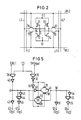
- FIG. 1 denotes a memory field which is constructed from a multiplicity of static memory cells, for example according to FIG. 2, in complementary circuit technology.
- each of these memory cells has two cross-coupled inverters, the first of which consists of the series connection of two field effect transistors T1 and T2, the second of the series connection of two field effect transistors T3 and T4.
- the source connections of the p-channel transistors T1 and T3 are connected to a connection 2 which is connected to a supply voltage of 5 V, for example.
- the source connections of the n-channel transistors T2 and T4 are connected to a connection 3 which is connected to the reference potential.
- the drain connections of T1 and T2 are connected to each other in a node 4, the gate connections of these transistors in a node 5.
- the drain connections of T3 and T4 are also connected to each other in node 5, the gate connections of T3 and T4 in node 4
- Nodes 4 and 5 are each connected to data lines L1 and L1 ⁇ via the source-drain paths of n-channel selection transistors T5 and T6, and to the data lines via the source-drain paths of n-channel selection transistors T8 and T7 L2 and L2 ⁇ .
- the gates of T5 and T6 are controlled via a word line WL1, the gates of T7 and T8 via a word line WL2.
- the memory cells are combined in rows and columns in memory array 1, in such a way that all memory cells in a row are connected to common word lines WL1 and WL2, while all memory cells in a column have common data line pairs L1, L1 ⁇ and L2, L2 ⁇ .
- the word lines WL1 of all lines of the memory array 1 are designated in FIG. 1 with WL P1 , the word lines WL2 of all lines with WL P2 .
- the data line pairs L1, L1 ⁇ all columns of the memory array are labeled LP P1
- the data line pairs L2, L2 ⁇ all columns are labeled LP P2 .
- DEA1 denotes a first input / output for data, DEA2 a second.
- a block 8 represents the row decoding for DEA1, a block 9 the row decoding for DEA2.
- the column decodings for DEA1 and DEA2 are labeled 10 and 11, respectively.
- the block 12 contains a sense amplifier and a write-in circuit which can optionally be connected to a data line pair L1, L1 ⁇ selected via the column decoding 10.
- a further block 13 contains a sense amplifier and a write-in circuit which can optionally be connected to a data line pair L2, L2 ⁇ selected via the column decoding 11.
- DEA1, DEA2 can also each consist of a multiplicity of inputs / outputs with corresponding input / output lines 14, 15.
- the blocks 12, 13 must then accordingly contain a multiplicity of sense amplifiers and write-in circuits.
- an address signal supplied to the input AZ1 of the row decoding 8 causes a specific word line WL1 to be selected from the word lines WL P1 . Furthermore, one causes Input AS1 of the column decoding 8 supplied address signal that a specific pair L1, L1 ⁇ is selected from the data line pairs LP P1 . Finally, a signal is fed to the input WR1 of the block 10, which in block 12 causes the connection of the sense amplifier or the write-in circuit to the selected data line pair.
- the addressing of a memory cell for the purpose of writing in or reading out a signal via DEA2 takes place with the aid of address signals which are fed to the inputs AZ2 of FIG. 9 and AS2 of FIG. 11 and a signal fed to the input WR2 which in block 13 activates the connection of the sense amplifier or the write-in circuit to the selected data line pair L2, L2 ⁇ .
- either or both of the word lines WL1 and WL2 can be addressed simultaneously, so that either one of the data line pairs, e.g. L1 and L1 ⁇ , or both data line pairs L1, L1 ⁇ and L2, L2 ⁇ are connected to the internal nodes 4, 5 of the memory cell via the transistors T5, T6 and T8, T7. If both word lines are addressed at the same time, the above-mentioned cases of conflict when writing signals can occur.
- a predetermined potential is applied to all data line pairs LP P1 and LP P2 , which is done for the data line pairs LP P1 via a precharge circuit 16 and for the data line pairs LP P2 via a precharge circuit 17.
- These precharge circuits contain, for example, p-channel transistors whose drain connections are connected to the individual data lines, while their source connections are connected to the supply voltage.
- the control connections of the p-channel transistors of the precharge circuit 16 are connected to an input 18, the control connections of the p-channel transistors of the precharge circuit 17 to an input 19.
- a data line is sufficient to explain the readout process pair, for example L1 and L1 ⁇ , with addressed word line WL1.
- L1, L1 ⁇ are precharged to the supply voltage by the precharge circuit.
- node 4 is at the supply voltage, for example, and node 5 is at the reference potential.
- the reading of the stored "1” now runs such that the data line L1 die is discharged to the reference potential via the transistor T6, while the data line L1 remains at the supply voltage.
- the resulting differential signal is evaluated as "1" via the sense amplifier of block 12 and output at the input / output DEA1.
- a clock circuit 20, whose input T is assigned an external voltage U T is used to derive internal clock voltages U D1 , U V1 , U D2 and U V2 from U T.
- U D1 causes the row decoding 8 and the column decoding 10, ie the address control for the input / output DEA1, to be activated, while U V1 activates the precharge circuit 16 via its input 18.
- U D2 causes the row decoding 9 and the column decoding 11, ie the address control for the input / output DEA2, to be activated, while U V2 activates the precharge circuit 17 via its input 19.
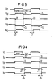
- the time course of the clock voltages mentioned which alternate between a lower voltage value corresponding to the reference voltage and an upper voltage value corresponding to the supply voltage, is shown in FIG. 3.
- the precharge circuits 16 and 17 are each activated, while the upper voltage values of U D1 and U D2 occur , the address controls for the inputs / outputs DEA1 and DEA2.
- the corresponding voltage increases at U V2 occur with a delay compared to the trailing edges 28 and 29 of U D2 by the time periods indicated by the double arrows 26 and 27.
- the address controls for DEA1 and DEA2 and the precharge circuits 16 and 17 are alternately actuated, with the address control 8 and 10 for DEA1 and the precharge circuit 17 being activated in a first clock phase PH1 of U T , while in In a second clock phase PH2, address control 9 and 11 for DEA2 and precharge circuit 16 are activated. Both clock phases add up to a complete clock period of U T.
- the address control of one input / output, for example DEA1 is activated, while the data line pairs, for example LP P2 , of the other input / output, for example DEA2, are precharged.
- the conflict situations mentioned at the outset which must be prevented in the conventional dual-port RAMs by logic gate circuits, can no longer occur.
- the clock circuit 20 can also be designed such that it can optionally be switched over to another operating mode in which a clock control of the address controls and the precharge circuits is carried out in accordance with Fig. 4 takes place.
- an input SM of the clock circuit 20 is assigned a signal U SM , which ensures an operating mode according to FIG. 3. If U SM is then switched off, the clock circuit 20 operates in an operating mode according to FIG. 4.
- the time dependencies of the internal clock voltages U D1 , U D2 , U V1 and U V2 that occur in the latter case are again shown below the external clock voltage U T.
- the address controls for the DEA1 and DEA2 on the one hand and the precharge circuits 16 and 17 on the other hand are controlled, with the address controls 8 and 10 for DEA1 and 9 and 11 for DEA2 in the first clock phase PH1 of U T are activated, while in the second clock phase PH2, the precharge circuits 16 and 17 are simultaneously activated.
- the address controls of both inputs / outputs or both precharge circuits 16 and 17 are activated simultaneously.
- the increases are also Clock voltage U V1 is advantageously delayed from the lower to the upper voltage value by the time periods indicated by the double arrows 30 and 31 compared to the previous trailing edges 32 and 33 of U D1 .
- the leading edges of U V2 lie behind the trailing edges 36 and 37 of U D2 by the time periods 34 and 35. This ensures that the address controls of the inputs / outputs are deactivated before the precharging of the data line pairs begins.
- FIG. 5 A preferred circuit design of the clock circuit 20 is shown in FIG. 5.
- This is a clock circuit which, according to the development of the invention, can optionally be switched to one of two operating modes. It contains two NAND gates 38, 39, the first inputs of which are labeled T and SM each correspond to the inputs of the same designation from FIG.
- the second inputs of 38 and 39 are connected to a terminal CS.
- the output of 38 is connected via an inverter 40 to a circuit node 41, which is connected to an output 43 via an amplifier 42.
- the node 41 is directly connected to the first input of a NOR gate 44 and connected to the second input thereof via an amplifier 45.
- the output of 44 is led to an output 47 via an amplifier 46.
- the node 41 is connected via an inverter 48 and a transmission gate 49 to a node 50, which in turn is connected to an output 52 via an amplifier 51.
- the node 50 is connected directly to the first input of a NOR gate 53 and connected to the second input of this gate via an amplifier 54, the output of which is connected to an output 56 via an amplifier 55.
- the transmission gate 49 consists of an n-channel transistor T9 and a p-channel transistor T10, which are inserted with their source-drain paths in each case between the output of the inverter 48 and the node 50.
- the gate connection of T9 is at the output of an inverter 57, which is connected downstream of the output of NOR gate 39, while the gate conclusion of T10 is at the output of an inverter 58 which is connected downstream of the inverter 57.
- a further transmission gate 59 is provided, which is formed from an n-channel transistor T11 and a p-channel transistor T12, which are inserted with their source-drain paths between the nodes 41 and 50.
- the gate connection of T11 lies at the output of inverter 58
- the gate connection of T12 lies at the output of inverter 57.
- connection CS is connected to a logic "1" and that a signal U SM is present at the input SM, which also corresponds to a logic "1"
- a signal U SM is present at the input SM, which also corresponds to a logic “1”
- the transmission gate 49 is turned on, while the transmission gate 59 remains blocked.
- Each clock pulse from U T is transmitted to the output of the inverter 40 and thus to the output 43 in a non-inverted manner, the internal clock voltage U D1 being able to be picked off at the output 43.
- the inverse voltage to U D1 is available as clock voltage U V1 , the time delays 22 and 23 arising from the running time of amplifier 45.
- the inverter 48 causes a voltage inverse to U D1 to occur at the output 52, which voltage represents the clock voltage U D2 .
- the clock voltage U V2 can be tapped at the output 56, the delays 26 and 27 arising from the running time of the amplifier 54.
- the clock voltages according to FIG. 3 are thus derived via the outputs 43, 47, 52 and 56.
- the transmission gate 59 is switched to conductive instead of 49 while the gate 49 is blocked.
- the nodes 41 and 50 are thus conductively connected to one another, so that the clock voltages U D2 and U V2 correspond completely to the clock voltages U D1 and U V1 . This results in the operating mode of the clock circuit 20 shown in FIG. 4.
- connection CS If a logical "0" is applied to the connection CS, then there are “1” signals at the outputs 47 and 56, regardless of the clock voltage U T , but "0" signals at the outputs 43 and 52, so that all data line pairs LP P1 and LP P2 are precharged.
- a clock circuit 20 which operates only in the operating mode according to FIG. 3, results from FIG. 5 in that the parts 39, 57, 58 and 59 are omitted and the transmission gate 49 by a conductive connection between the output of 48 and the node 50 is replaced.
Landscapes
- Engineering & Computer Science (AREA)
- Microelectronics & Electronic Packaging (AREA)
- Computer Hardware Design (AREA)
- Static Random-Access Memory (AREA)
- Semiconductor Memories (AREA)
- Techniques For Improving Reliability Of Storages (AREA)
Priority Applications (1)
| Application Number | Priority Date | Filing Date | Title |
|---|---|---|---|
| AT88100197T ATE89946T1 (de) | 1987-01-23 | 1988-01-08 | Halbleiterspeicher mit wahlfreiem zugriff ueber zwei getrennte ein/ausgaenge. |
Applications Claiming Priority (2)
| Application Number | Priority Date | Filing Date | Title |
|---|---|---|---|
| DE3701976 | 1987-01-23 | ||
| DE3701976 | 1987-01-23 |
Publications (3)
| Publication Number | Publication Date |
|---|---|
| EP0275884A2 true EP0275884A2 (fr) | 1988-07-27 |
| EP0275884A3 EP0275884A3 (en) | 1990-12-05 |
| EP0275884B1 EP0275884B1 (fr) | 1993-05-26 |
Family
ID=6319407
Family Applications (1)
| Application Number | Title | Priority Date | Filing Date |
|---|---|---|---|
| EP88100197A Expired - Lifetime EP0275884B1 (fr) | 1987-01-23 | 1988-01-08 | Mémoire à semi-conducteurs accessible sur deux entrées et deux sorties différentes |
Country Status (5)
| Country | Link |
|---|---|
| US (1) | US4860263A (fr) |
| EP (1) | EP0275884B1 (fr) |
| JP (1) | JPS63188887A (fr) |
| AT (1) | ATE89946T1 (fr) |
| DE (1) | DE3881222D1 (fr) |
Cited By (2)
| Publication number | Priority date | Publication date | Assignee | Title |
|---|---|---|---|---|
| EP0363984A3 (fr) * | 1988-10-14 | 1991-04-17 | Siemens Aktiengesellschaft | Circuit d'amplification d'adresse à autoverrouillage et sécurité contre l'adressage multiple pour application dans des GaAs-RAMs statiques |
| EP0755538A4 (fr) * | 1994-04-15 | 1998-05-20 | Sarnoff David Res Center | Appareil et procede d'actualisation d'informations dans une memoire microprogrammable |
Families Citing this family (13)
| Publication number | Priority date | Publication date | Assignee | Title |
|---|---|---|---|---|
| US4975872A (en) * | 1988-11-17 | 1990-12-04 | Matsushita Electric Industrial Co., Ltd. | Dual port memory device with tag bit marking |
| FR2639461A1 (fr) * | 1988-11-18 | 1990-05-25 | Labo Electronique Physique | Arrangement bidimensionnel de points memoire et structure de reseaux de neurones utilisant un tel arrangement |
| US5014247A (en) * | 1988-12-19 | 1991-05-07 | Advanced Micro Devices, Inc. | System for accessing the same memory location by two different devices |
| JPH02177195A (ja) * | 1988-12-28 | 1990-07-10 | Fujitsu Ltd | 2ポートスタテックram |
| US5210701A (en) * | 1989-05-15 | 1993-05-11 | Cascade Design Automation Corporation | Apparatus and method for designing integrated circuit modules |
| US5235543A (en) * | 1989-12-29 | 1993-08-10 | Intel Corporation | Dual port static memory with one cycle read-modify-write |
| JPH03224197A (ja) * | 1990-01-30 | 1991-10-03 | Toshiba Corp | 多ポートram及び情報処理装置 |
| US5003509A (en) * | 1990-03-27 | 1991-03-26 | National Semiconductor Corp. | Multi-port, bipolar-CMOS memory cell |
| JP2965043B2 (ja) * | 1990-04-10 | 1999-10-18 | 三菱電機株式会社 | デュアルポートメモリ |
| US5465344A (en) * | 1990-08-20 | 1995-11-07 | Matsushita Electric Industrial Co., Ltd. | Microprocessor with dual-port cache memory for reducing penalty of consecutive memory address accesses |
| JP2673390B2 (ja) * | 1991-03-13 | 1997-11-05 | 三菱電機株式会社 | マルチポートメモリ |
| US5371877A (en) * | 1991-12-31 | 1994-12-06 | Apple Computer, Inc. | Apparatus for alternatively accessing single port random access memories to implement dual port first-in first-out memory |
| US5504503A (en) * | 1993-12-03 | 1996-04-02 | Lsi Logic Corporation | High speed signal conversion method and device |
Family Cites Families (8)
| Publication number | Priority date | Publication date | Assignee | Title |
|---|---|---|---|---|
| JPS56165983A (en) * | 1980-05-26 | 1981-12-19 | Toshiba Corp | Semiconductor storage device |
| US4395765A (en) * | 1981-04-23 | 1983-07-26 | Bell Telephone Laboratories, Incorporated | Multiport memory array |
| US4541076A (en) * | 1982-05-13 | 1985-09-10 | Storage Technology Corporation | Dual port CMOS random access memory |
| JPS59198584A (ja) * | 1983-04-22 | 1984-11-10 | Nec Corp | マルチアクセス記憶装置 |
| US4520465A (en) * | 1983-05-05 | 1985-05-28 | Motorola, Inc. | Method and apparatus for selectively precharging column lines of a memory |
| JPS6072020A (ja) * | 1983-09-29 | 1985-04-24 | Nec Corp | デュアルポ−トメモリ回路 |
| JPS60140924A (ja) * | 1983-12-27 | 1985-07-25 | Nec Corp | 半導体回路 |
| US4623990A (en) * | 1984-10-31 | 1986-11-18 | Advanced Micro Devices, Inc. | Dual-port read/write RAM with single array |
-
1988
- 1988-01-08 EP EP88100197A patent/EP0275884B1/fr not_active Expired - Lifetime
- 1988-01-08 AT AT88100197T patent/ATE89946T1/de not_active IP Right Cessation
- 1988-01-08 DE DE8888100197T patent/DE3881222D1/de not_active Expired - Fee Related
- 1988-01-20 JP JP63011828A patent/JPS63188887A/ja active Pending
- 1988-01-25 US US07/147,451 patent/US4860263A/en not_active Expired - Lifetime
Cited By (2)
| Publication number | Priority date | Publication date | Assignee | Title |
|---|---|---|---|---|
| EP0363984A3 (fr) * | 1988-10-14 | 1991-04-17 | Siemens Aktiengesellschaft | Circuit d'amplification d'adresse à autoverrouillage et sécurité contre l'adressage multiple pour application dans des GaAs-RAMs statiques |
| EP0755538A4 (fr) * | 1994-04-15 | 1998-05-20 | Sarnoff David Res Center | Appareil et procede d'actualisation d'informations dans une memoire microprogrammable |
Also Published As
| Publication number | Publication date |
|---|---|
| US4860263A (en) | 1989-08-22 |
| JPS63188887A (ja) | 1988-08-04 |
| ATE89946T1 (de) | 1993-06-15 |
| DE3881222D1 (de) | 1993-07-01 |
| EP0275884A3 (en) | 1990-12-05 |
| EP0275884B1 (fr) | 1993-05-26 |
Similar Documents
| Publication | Publication Date | Title |
|---|---|---|
| DE3686626T2 (de) | Speicherzelle. | |
| DE3588247T2 (de) | Dynamischer Halbleiterspeicher mit einer statischen Datenspeicherzelle | |
| DE68921599T2 (de) | Verstärkungstaktsignalgenerator. | |
| DE4238063C2 (de) | Integrierte Speicherzellenschaltung mit Set-/Reset-Funktion | |
| EP0275884B1 (fr) | Mémoire à semi-conducteurs accessible sur deux entrées et deux sorties différentes | |
| EP0393435B1 (fr) | Cellule de mémoire statique | |
| DE69216695T2 (de) | Halbleiterspeicher | |
| DE4238062C2 (de) | Multiport-Speichereinrichtung | |
| DE4324651C2 (de) | Boosting-Schaltung und Verwendung der Boosting-Schaltung | |
| DE3886938T2 (de) | Reprogrammierbare logische Sicherung für logische Anordnungen, basierend auf einer 6-Elementen-SRAM-Zelle. | |
| DE19944727B4 (de) | Integrierte Schaltung und synchrones Halbleiterspeicherbauelement mit einer Takterzeugungsschaltung | |
| DE4108996C2 (de) | Halbleiterspeichereinrichtung | |
| DE10330920B4 (de) | Statische Speicherzelle mit Dual-Port und zugehöriger Halbleiterspeicherbaustein | |
| EP0224887B1 (fr) | Matrice de portes en technologie CMOS | |
| DE3104880C2 (de) | Speicher für wahlfreien Zugriff | |
| DE3939849A1 (de) | Halbleiterspeichereinrichtung mit einem geteilten leseverstaerker und verfahren zu deren betrieb | |
| DE10121708B4 (de) | Halbleiterspeichereinrichtung und Verfahren zum Ändern von Ausgangsdaten dieser Einrichtung | |
| DE19651340C2 (de) | Halbleiterspeichervorrichtung | |
| DE10053507B4 (de) | Halbleiterspeichervorrichtung | |
| DE68922738T2 (de) | Hochintegrierter Halbleiterspeicher mit Mehrfachzugang. | |
| DE19531021C2 (de) | Datenleseschaltung | |
| EP0052669A1 (fr) | Mémoire à semi-conducteur hautement intégrée et adressage multiple | |
| DE69219383T2 (de) | Zwei-Tor-integrierte Halbleiterspeicherschaltung | |
| DE3884460T2 (de) | Intergrierte Halbleiterschaltung. | |
| DE19743347C2 (de) | RS-Flip-Flop mit Enable-Eingängen |
Legal Events
| Date | Code | Title | Description |
|---|---|---|---|
| PUAI | Public reference made under article 153(3) epc to a published international application that has entered the european phase |
Free format text: ORIGINAL CODE: 0009012 |
|
| AK | Designated contracting states |
Kind code of ref document: A2 Designated state(s): AT DE FR GB IT NL |
|
| PUAL | Search report despatched |
Free format text: ORIGINAL CODE: 0009013 |
|
| AK | Designated contracting states |
Kind code of ref document: A3 Designated state(s): AT DE FR GB IT NL |
|
| 17P | Request for examination filed |
Effective date: 19901205 |
|
| 17Q | First examination report despatched |
Effective date: 19920310 |
|
| GRAA | (expected) grant |
Free format text: ORIGINAL CODE: 0009210 |
|
| AK | Designated contracting states |
Kind code of ref document: B1 Designated state(s): AT DE FR GB IT NL |
|
| REF | Corresponds to: |
Ref document number: 89946 Country of ref document: AT Date of ref document: 19930615 Kind code of ref document: T |
|
| REF | Corresponds to: |
Ref document number: 3881222 Country of ref document: DE Date of ref document: 19930701 |
|
| ET | Fr: translation filed | ||
| ITF | It: translation for a ep patent filed | ||
| GBT | Gb: translation of ep patent filed (gb section 77(6)(a)/1977) |
Effective date: 19930804 |
|
| PGFP | Annual fee paid to national office [announced via postgrant information from national office to epo] |
Ref country code: AT Payment date: 19931222 Year of fee payment: 7 |
|
| PGFP | Annual fee paid to national office [announced via postgrant information from national office to epo] |
Ref country code: NL Payment date: 19940131 Year of fee payment: 7 |
|
| PLBE | No opposition filed within time limit |
Free format text: ORIGINAL CODE: 0009261 |
|
| STAA | Information on the status of an ep patent application or granted ep patent |
Free format text: STATUS: NO OPPOSITION FILED WITHIN TIME LIMIT |
|
| 26N | No opposition filed | ||
| PG25 | Lapsed in a contracting state [announced via postgrant information from national office to epo] |
Ref country code: AT Effective date: 19950108 |
|
| PG25 | Lapsed in a contracting state [announced via postgrant information from national office to epo] |
Ref country code: NL Effective date: 19950801 |
|
| NLV4 | Nl: lapsed or anulled due to non-payment of the annual fee |
Effective date: 19950801 |
|
| PGFP | Annual fee paid to national office [announced via postgrant information from national office to epo] |
Ref country code: DE Payment date: 20010319 Year of fee payment: 14 |
|
| REG | Reference to a national code |
Ref country code: GB Ref legal event code: IF02 |
|
| PGFP | Annual fee paid to national office [announced via postgrant information from national office to epo] |
Ref country code: GB Payment date: 20020110 Year of fee payment: 15 |
|
| PGFP | Annual fee paid to national office [announced via postgrant information from national office to epo] |
Ref country code: FR Payment date: 20020124 Year of fee payment: 15 |
|
| PG25 | Lapsed in a contracting state [announced via postgrant information from national office to epo] |
Ref country code: DE Free format text: LAPSE BECAUSE OF NON-PAYMENT OF DUE FEES Effective date: 20020801 |
|
| PG25 | Lapsed in a contracting state [announced via postgrant information from national office to epo] |
Ref country code: GB Free format text: LAPSE BECAUSE OF NON-PAYMENT OF DUE FEES Effective date: 20030108 |
|
| GBPC | Gb: european patent ceased through non-payment of renewal fee |
Effective date: 20030108 |
|
| PG25 | Lapsed in a contracting state [announced via postgrant information from national office to epo] |
Ref country code: FR Free format text: LAPSE BECAUSE OF NON-PAYMENT OF DUE FEES Effective date: 20030930 |
|
| REG | Reference to a national code |
Ref country code: FR Ref legal event code: ST |
|
| PG25 | Lapsed in a contracting state [announced via postgrant information from national office to epo] |
Ref country code: IT Free format text: LAPSE BECAUSE OF NON-PAYMENT OF DUE FEES;WARNING: LAPSES OF ITALIAN PATENTS WITH EFFECTIVE DATE BEFORE 2007 MAY HAVE OCCURRED AT ANY TIME BEFORE 2007. THE CORRECT EFFECTIVE DATE MAY BE DIFFERENT FROM THE ONE RECORDED. Effective date: 20050108 |