EP0265833A1 - Composant semi-conducteur comprenant au moins un MOSFET de puissance - Google Patents
Composant semi-conducteur comprenant au moins un MOSFET de puissance Download PDFInfo
- Publication number
- EP0265833A1 EP0265833A1 EP87115443A EP87115443A EP0265833A1 EP 0265833 A1 EP0265833 A1 EP 0265833A1 EP 87115443 A EP87115443 A EP 87115443A EP 87115443 A EP87115443 A EP 87115443A EP 0265833 A1 EP0265833 A1 EP 0265833A1
- Authority
- EP
- European Patent Office
- Prior art keywords
- conductor tracks
- conductor
- semiconductor
- semiconductor component
- component according
- Prior art date
- Legal status (The legal status is an assumption and is not a legal conclusion. Google has not performed a legal analysis and makes no representation as to the accuracy of the status listed.)
- Granted
Links
Images
Classifications
-
- H—ELECTRICITY
- H01—ELECTRIC ELEMENTS
- H01L—SEMICONDUCTOR DEVICES NOT COVERED BY CLASS H10
- H01L23/00—Details of semiconductor or other solid state devices
- H01L23/58—Structural electrical arrangements for semiconductor devices not otherwise provided for, e.g. in combination with batteries
- H01L23/64—Impedance arrangements
- H01L23/645—Inductive arrangements
-
- H—ELECTRICITY
- H01—ELECTRIC ELEMENTS
- H01L—SEMICONDUCTOR DEVICES NOT COVERED BY CLASS H10
- H01L24/00—Arrangements for connecting or disconnecting semiconductor or solid-state bodies; Methods or apparatus related thereto
- H01L24/01—Means for bonding being attached to, or being formed on, the surface to be connected, e.g. chip-to-package, die-attach, "first-level" interconnects; Manufacturing methods related thereto
- H01L24/42—Wire connectors; Manufacturing methods related thereto
- H01L24/47—Structure, shape, material or disposition of the wire connectors after the connecting process
- H01L24/49—Structure, shape, material or disposition of the wire connectors after the connecting process of a plurality of wire connectors
-
- H—ELECTRICITY
- H01—ELECTRIC ELEMENTS
- H01L—SEMICONDUCTOR DEVICES NOT COVERED BY CLASS H10
- H01L25/00—Assemblies consisting of a plurality of individual semiconductor or other solid state devices ; Multistep manufacturing processes thereof
- H01L25/03—Assemblies consisting of a plurality of individual semiconductor or other solid state devices ; Multistep manufacturing processes thereof all the devices being of a type provided for in the same subgroup of groups H01L27/00 - H01L33/00, or in a single subclass of H10K, H10N, e.g. assemblies of rectifier diodes
- H01L25/04—Assemblies consisting of a plurality of individual semiconductor or other solid state devices ; Multistep manufacturing processes thereof all the devices being of a type provided for in the same subgroup of groups H01L27/00 - H01L33/00, or in a single subclass of H10K, H10N, e.g. assemblies of rectifier diodes the devices not having separate containers
- H01L25/07—Assemblies consisting of a plurality of individual semiconductor or other solid state devices ; Multistep manufacturing processes thereof all the devices being of a type provided for in the same subgroup of groups H01L27/00 - H01L33/00, or in a single subclass of H10K, H10N, e.g. assemblies of rectifier diodes the devices not having separate containers the devices being of a type provided for in group H01L29/00
- H01L25/072—Assemblies consisting of a plurality of individual semiconductor or other solid state devices ; Multistep manufacturing processes thereof all the devices being of a type provided for in the same subgroup of groups H01L27/00 - H01L33/00, or in a single subclass of H10K, H10N, e.g. assemblies of rectifier diodes the devices not having separate containers the devices being of a type provided for in group H01L29/00 the devices being arranged next to each other
-
- H—ELECTRICITY
- H01—ELECTRIC ELEMENTS
- H01L—SEMICONDUCTOR DEVICES NOT COVERED BY CLASS H10
- H01L2224/00—Indexing scheme for arrangements for connecting or disconnecting semiconductor or solid-state bodies and methods related thereto as covered by H01L24/00
- H01L2224/01—Means for bonding being attached to, or being formed on, the surface to be connected, e.g. chip-to-package, die-attach, "first-level" interconnects; Manufacturing methods related thereto
- H01L2224/02—Bonding areas; Manufacturing methods related thereto
- H01L2224/04—Structure, shape, material or disposition of the bonding areas prior to the connecting process
- H01L2224/06—Structure, shape, material or disposition of the bonding areas prior to the connecting process of a plurality of bonding areas
- H01L2224/0601—Structure
- H01L2224/0603—Bonding areas having different sizes, e.g. different heights or widths
-
- H—ELECTRICITY
- H01—ELECTRIC ELEMENTS
- H01L—SEMICONDUCTOR DEVICES NOT COVERED BY CLASS H10
- H01L2224/00—Indexing scheme for arrangements for connecting or disconnecting semiconductor or solid-state bodies and methods related thereto as covered by H01L24/00
- H01L2224/01—Means for bonding being attached to, or being formed on, the surface to be connected, e.g. chip-to-package, die-attach, "first-level" interconnects; Manufacturing methods related thereto
- H01L2224/42—Wire connectors; Manufacturing methods related thereto
- H01L2224/47—Structure, shape, material or disposition of the wire connectors after the connecting process
- H01L2224/48—Structure, shape, material or disposition of the wire connectors after the connecting process of an individual wire connector
- H01L2224/481—Disposition
- H01L2224/48151—Connecting between a semiconductor or solid-state body and an item not being a semiconductor or solid-state body, e.g. chip-to-substrate, chip-to-passive
- H01L2224/48221—Connecting between a semiconductor or solid-state body and an item not being a semiconductor or solid-state body, e.g. chip-to-substrate, chip-to-passive the body and the item being stacked
- H01L2224/48225—Connecting between a semiconductor or solid-state body and an item not being a semiconductor or solid-state body, e.g. chip-to-substrate, chip-to-passive the body and the item being stacked the item being non-metallic, e.g. insulating substrate with or without metallisation
- H01L2224/48227—Connecting between a semiconductor or solid-state body and an item not being a semiconductor or solid-state body, e.g. chip-to-substrate, chip-to-passive the body and the item being stacked the item being non-metallic, e.g. insulating substrate with or without metallisation connecting the wire to a bond pad of the item
-
- H—ELECTRICITY
- H01—ELECTRIC ELEMENTS
- H01L—SEMICONDUCTOR DEVICES NOT COVERED BY CLASS H10
- H01L2224/00—Indexing scheme for arrangements for connecting or disconnecting semiconductor or solid-state bodies and methods related thereto as covered by H01L24/00
- H01L2224/01—Means for bonding being attached to, or being formed on, the surface to be connected, e.g. chip-to-package, die-attach, "first-level" interconnects; Manufacturing methods related thereto
- H01L2224/42—Wire connectors; Manufacturing methods related thereto
- H01L2224/47—Structure, shape, material or disposition of the wire connectors after the connecting process
- H01L2224/49—Structure, shape, material or disposition of the wire connectors after the connecting process of a plurality of wire connectors
- H01L2224/491—Disposition
- H01L2224/4911—Disposition the connectors being bonded to at least one common bonding area, e.g. daisy chain
- H01L2224/49111—Disposition the connectors being bonded to at least one common bonding area, e.g. daisy chain the connectors connecting two common bonding areas, e.g. Litz or braid wires
-
- H—ELECTRICITY
- H01—ELECTRIC ELEMENTS
- H01L—SEMICONDUCTOR DEVICES NOT COVERED BY CLASS H10
- H01L2224/00—Indexing scheme for arrangements for connecting or disconnecting semiconductor or solid-state bodies and methods related thereto as covered by H01L24/00
- H01L2224/01—Means for bonding being attached to, or being formed on, the surface to be connected, e.g. chip-to-package, die-attach, "first-level" interconnects; Manufacturing methods related thereto
- H01L2224/42—Wire connectors; Manufacturing methods related thereto
- H01L2224/47—Structure, shape, material or disposition of the wire connectors after the connecting process
- H01L2224/49—Structure, shape, material or disposition of the wire connectors after the connecting process of a plurality of wire connectors
- H01L2224/491—Disposition
- H01L2224/4911—Disposition the connectors being bonded to at least one common bonding area, e.g. daisy chain
- H01L2224/49113—Disposition the connectors being bonded to at least one common bonding area, e.g. daisy chain the connectors connecting different bonding areas on the semiconductor or solid-state body to a common bonding area outside the body, e.g. converging wires
-
- H—ELECTRICITY
- H01—ELECTRIC ELEMENTS
- H01L—SEMICONDUCTOR DEVICES NOT COVERED BY CLASS H10
- H01L2224/00—Indexing scheme for arrangements for connecting or disconnecting semiconductor or solid-state bodies and methods related thereto as covered by H01L24/00
- H01L2224/01—Means for bonding being attached to, or being formed on, the surface to be connected, e.g. chip-to-package, die-attach, "first-level" interconnects; Manufacturing methods related thereto
- H01L2224/42—Wire connectors; Manufacturing methods related thereto
- H01L2224/47—Structure, shape, material or disposition of the wire connectors after the connecting process
- H01L2224/49—Structure, shape, material or disposition of the wire connectors after the connecting process of a plurality of wire connectors
- H01L2224/491—Disposition
- H01L2224/4912—Layout
- H01L2224/49175—Parallel arrangements
-
- H—ELECTRICITY
- H01—ELECTRIC ELEMENTS
- H01L—SEMICONDUCTOR DEVICES NOT COVERED BY CLASS H10
- H01L24/00—Arrangements for connecting or disconnecting semiconductor or solid-state bodies; Methods or apparatus related thereto
- H01L24/01—Means for bonding being attached to, or being formed on, the surface to be connected, e.g. chip-to-package, die-attach, "first-level" interconnects; Manufacturing methods related thereto
- H01L24/42—Wire connectors; Manufacturing methods related thereto
- H01L24/47—Structure, shape, material or disposition of the wire connectors after the connecting process
- H01L24/48—Structure, shape, material or disposition of the wire connectors after the connecting process of an individual wire connector
-
- H—ELECTRICITY
- H01—ELECTRIC ELEMENTS
- H01L—SEMICONDUCTOR DEVICES NOT COVERED BY CLASS H10
- H01L2924/00—Indexing scheme for arrangements or methods for connecting or disconnecting semiconductor or solid-state bodies as covered by H01L24/00
- H01L2924/0001—Technical content checked by a classifier
- H01L2924/00014—Technical content checked by a classifier the subject-matter covered by the group, the symbol of which is combined with the symbol of this group, being disclosed without further technical details
-
- H—ELECTRICITY
- H01—ELECTRIC ELEMENTS
- H01L—SEMICONDUCTOR DEVICES NOT COVERED BY CLASS H10
- H01L2924/00—Indexing scheme for arrangements or methods for connecting or disconnecting semiconductor or solid-state bodies as covered by H01L24/00
- H01L2924/01—Chemical elements
- H01L2924/01005—Boron [B]
-
- H—ELECTRICITY
- H01—ELECTRIC ELEMENTS
- H01L—SEMICONDUCTOR DEVICES NOT COVERED BY CLASS H10
- H01L2924/00—Indexing scheme for arrangements or methods for connecting or disconnecting semiconductor or solid-state bodies as covered by H01L24/00
- H01L2924/01—Chemical elements
- H01L2924/01013—Aluminum [Al]
-
- H—ELECTRICITY
- H01—ELECTRIC ELEMENTS
- H01L—SEMICONDUCTOR DEVICES NOT COVERED BY CLASS H10
- H01L2924/00—Indexing scheme for arrangements or methods for connecting or disconnecting semiconductor or solid-state bodies as covered by H01L24/00
- H01L2924/01—Chemical elements
- H01L2924/01058—Cerium [Ce]
-
- H—ELECTRICITY
- H01—ELECTRIC ELEMENTS
- H01L—SEMICONDUCTOR DEVICES NOT COVERED BY CLASS H10
- H01L2924/00—Indexing scheme for arrangements or methods for connecting or disconnecting semiconductor or solid-state bodies as covered by H01L24/00
- H01L2924/10—Details of semiconductor or other solid state devices to be connected
- H01L2924/11—Device type
- H01L2924/13—Discrete devices, e.g. 3 terminal devices
- H01L2924/1304—Transistor
- H01L2924/1306—Field-effect transistor [FET]
- H01L2924/13091—Metal-Oxide-Semiconductor Field-Effect Transistor [MOSFET]
-
- H—ELECTRICITY
- H01—ELECTRIC ELEMENTS
- H01L—SEMICONDUCTOR DEVICES NOT COVERED BY CLASS H10
- H01L2924/00—Indexing scheme for arrangements or methods for connecting or disconnecting semiconductor or solid-state bodies as covered by H01L24/00
- H01L2924/19—Details of hybrid assemblies other than the semiconductor or other solid state devices to be connected
- H01L2924/1901—Structure
- H01L2924/1904—Component type
- H01L2924/19043—Component type being a resistor
-
- H—ELECTRICITY
- H01—ELECTRIC ELEMENTS
- H01L—SEMICONDUCTOR DEVICES NOT COVERED BY CLASS H10
- H01L2924/00—Indexing scheme for arrangements or methods for connecting or disconnecting semiconductor or solid-state bodies as covered by H01L24/00
- H01L2924/30—Technical effects
- H01L2924/301—Electrical effects
- H01L2924/30107—Inductance
Definitions
- the invention relates to a semiconductor component with at least one power MOSFET, the semiconductor body of which has a source contact and a source connection connected to it, and a gate contact and a gate connection connected to it.
- Such semiconductor components are turned on by a control voltage applied between the source contact and the gate contact.
- the control voltage is in practice placed between the source connection and the gate connection.
- the wire serving as the source connection has a self-inductance which has the effect that the load current which changes over time when the MOSFET is switched on or off induces a voltage in the inductance which counteracts the control voltage with a switching delay. If you connect several power MOSFETs in parallel and control them together from a single voltage source, the aforementioned inductance leads to high-frequency vibrations with amplitudes occurring in the control circuit due to inevitable component tolerances, which can destroy the FET input.
- the oscillation frequency is largely determined by the aforementioned inductance of the source connection and also by other parasitic network and component parameters. The amplitude of the vibration is increased by the steepness of the MOSFET.
- the invention has for its object to develop a semiconductor device of the type mentioned in such a way that the aforementioned disadvantageous effect of the inductance of the source connection is further reduced and the vibrations mentioned in parallel MOSFET are avoided even with fast switching in the order of magnitude below a microsecond.
- auxiliary connection connected to the source contact, which is magnetically decoupled at least partially from the source connection.
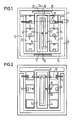
- FIGS. 1 to 3 show top views of three exemplary embodiments, each with parallel connected MOSFET semiconductor bodies.
- the semiconductor component according to FIG. 1 is constructed on an insulating, thermally conductive substrate 1.
- the substrate can consist, for example, of a known aluminum oxide ceramic. It is provided with first conductor tracks 2, 12, second conductor tracks 3, 13 and third conductor tracks 4, 14. These conductor tracks lie parallel to one another and are arranged mirror-symmetrically to an axis of symmetry 24 forming a longitudinal axis of the substrate 1.
- the substrate is also provided with a fourth conductor track 5, which sits on the axis of symmetry 24.
- the first conductor tracks 2, 12 and the second conductor tracks 3, 13 are conductively connected to one another by bridges 15 and 16, respectively.
- the third conductor tracks 4, 14 are electrically connected to one another by bridges 17, 18.
- the conductor tracks 2, 12 together with the bridge 16 form a first U-shaped conductor, while the conductor tracks 3, 13 form a second U-shaped conductor with the bridge 15. Both U-shaped conductors are rotated against each other by 180 ° and nested in one another on the substrate.
- the semiconductor bodies 6 are each provided with a gate contact 7 and a source contact 8.
- the source contacts 8 are z. B. connected via bond wires 9 to the second conductor tracks 3, 13.
- the conductor tracks 3, 13 together with the bridge 15 and the bonding wires 9 form the source connection.
- the gate contacts 7 are each connected to the third conductor tracks 4, 14 via one or more bond wires 11. Together with the bridges 17, 18 and the bonding wires 11, these conductor tracks form the gate connection of the semiconductor component.
- the conductor tracks 2, 12 serve as a drain connection.
- the source contacts 8 are connected to the conductor track 5 via bond wires 10.
- the bond wires 10 together with the conductor track 5 form an auxiliary connection for controlling the MOSFET connected in parallel. To keep the bond wires short, they are at right angles to the conductor tracks.
- the semiconductor component is switched on by a control voltage applied between the gate connection and auxiliary connection.
- Such a semiconductor device can, for. B. switch through completely within 100 ns without high-frequency vibrations occurring in the control circuit.
- the magnetic decoupling is the better the further the bonding wires 9 carrying the load current are from the bonding wire 10.
- the arrangement is optimal when, as shown, the bonding wires 9 and 10 protrude from the source contact 8 on opposite sides.
- a further improvement in the control behavior can be achieved in that the conductor systems belonging to the control circuit, consisting of the bond wires 10, 11 and essentially the conductor tracks 4, or 14, are arranged close to one another and are at least partially parallel to one another.
- the inductance of the control circuit can thus be reduced.
- the bonding wires and conductor tracks mentioned can be arranged as close to one another as is possible for insulation and manufacturing reasons.
- the semiconductor body 6 are arranged on the conductor tracks 2, 12 such that the bond wires 10 and 11 are relatively far apart.
- the semiconductor bodies are rotated by 90 degrees compared to the exemplary embodiment according to FIG. A spatially adjacent arrangement of the bond wires 10 and 11 belonging to the control circuit is thus possible if the source and gate contacts lie opposite one another at the edge of the semiconductor body.
- the drain connections, source connections and gate connections as well as the auxiliary connections are connected to housing connections 19, 20, 22 and 23.
- 19 forms the source housing connection, 20 the drain housing connection, 22 the gate housing connection and 23 the auxiliary housing connection.
- These housing connections lead from a housing enveloping the substrate, the semiconductor bodies, the conductor tracks and the bonding wires and are for connection to external voltage sources or an ex internal load determined.
- the housing connections 19, 20 are symmetrical to the axis of symmetry 24 on the bridges 15 or respectively. 16 or in other words on the yokes of the U-shaped conductor systems.
- the housing connections 22, 23 sit in the middle of the longitudinal extent of the third or fourth conductor track. Sit the semiconductor body 6 evenly distributed on the conductor tracks 2, 12, you get largely uniform current distribution and uniform switching conditions for all MOSFET.
- the exemplary embodiments according to FIGS. 1 and 2 each have six semiconductor bodies. However, it is also possible to use the same principle to construct semiconductor components with fewer or more, preferably an even number, of semiconductor bodies. It is also possible to construct semiconductor components according to the principle described, which contains, for example, only a single arrangement lying on one side of the axis of symmetry. It is also conceivable to build semiconductor components with only a single semiconductor body according to the principle shown.
- first and second conductor tracks 2, 12 shown in FIGS. 1 and 2; 3, 13 these can also be interlocked with one another in the manner of finger structures.
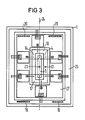
- Figure 3 Another embodiment is shown in Figure 3.
- the first and the second conductor tracks are each formed as closed rings 26 and 27 and arranged one inside the other.
- the third conductor tracks 4, 14, 17, 18, which also form a ring, lie in the ring 27.
- Two of the semiconductor bodies lie on the axis of symmetry 24.
- the housing connections 19, 20 have been divided here and contact the rings 26, 27 on both sides of these semiconductor bodies. They are at right angles and symmetrical to the axis of symmetry 24.
- each semiconductor body may be turned on a resistor 25 ( Figure 2).
- resistor 25 can e.g. B. be a doped semiconductor chip, which is soldered onto the conductor tracks 4, 14, respectively. The bond wire 11 then contacts the top of the plate.
Applications Claiming Priority (2)
| Application Number | Priority Date | Filing Date | Title |
|---|---|---|---|
| DE3635956 | 1986-10-22 | ||
| DE3635956 | 1986-10-22 |
Publications (2)
| Publication Number | Publication Date |
|---|---|
| EP0265833A1 true EP0265833A1 (fr) | 1988-05-04 |
| EP0265833B1 EP0265833B1 (fr) | 1991-07-24 |
Family
ID=6312248
Family Applications (1)
| Application Number | Title | Priority Date | Filing Date |
|---|---|---|---|
| EP87115443A Expired - Lifetime EP0265833B1 (fr) | 1986-10-22 | 1987-10-21 | Composant semi-conducteur comprenant au moins un MOSFET de puissance |
Country Status (3)
| Country | Link |
|---|---|
| EP (1) | EP0265833B1 (fr) |
| JP (1) | JPH088269B2 (fr) |
| DE (1) | DE3771648D1 (fr) |
Cited By (9)
| Publication number | Priority date | Publication date | Assignee | Title |
|---|---|---|---|---|
| FR2652983A1 (fr) * | 1989-10-11 | 1991-04-12 | Alsthom Gec | Montage en cascade d'etages de transistors en parallele realise en circuit hybride. |
| US5025296A (en) * | 1988-02-29 | 1991-06-18 | Motorola, Inc. | Center tapped FET |
| EP0499707A1 (fr) * | 1991-02-22 | 1992-08-26 | Asea Brown Boveri Ag | Composant semi-conducteur de puissance à commande d'extinction |
| DE4227063A1 (de) * | 1992-08-15 | 1994-02-17 | Abb Research Ltd | Abschaltbares Hochleistungs-Halbleiterbauelement |
| EP1028465A2 (fr) * | 1999-02-05 | 2000-08-16 | Kabushiki Kaisha Toyoda Jidoshokki Seisakusho | Module à semi-conducteur |
| WO2002058150A1 (fr) * | 2001-01-19 | 2002-07-25 | Siemens Aktiengesellschaft | Circuit a composants semi-conducteurs agences dans des puces |
| US6507108B1 (en) | 1999-09-08 | 2003-01-14 | Ixys Semiconductor Gmbh | Power semiconductor module |
| US8410591B2 (en) | 2007-03-15 | 2013-04-02 | Infineon Technologies Ag | Semiconductor module with multiple semiconductor chips |
| EP4297087A1 (fr) * | 2022-06-24 | 2023-12-27 | Airbus S.A.S. | Module électronique de puissance avec dispositifs électroniques de puissance connectés en parallèle |
Families Citing this family (6)
| Publication number | Priority date | Publication date | Assignee | Title |
|---|---|---|---|---|
| JPH0832060A (ja) * | 1994-07-13 | 1996-02-02 | Hitachi Ltd | 半導体集積回路装置およびその製造方法 |
| DE19927285C2 (de) * | 1999-06-15 | 2003-05-22 | Eupec Gmbh & Co Kg | Niederinduktives Halbleiterbauelement |
| JP5548141B2 (ja) * | 2011-01-07 | 2014-07-16 | 日立オートモティブシステムズ株式会社 | シートベルトリトラクタの制御装置 |
| JP5876970B2 (ja) * | 2012-06-19 | 2016-03-02 | アーベーベー・テクノロジー・アーゲー | 複数のパワートランジスタを搭載するための基板、およびパワー半導体モジュール |
| US9426883B2 (en) | 2014-01-30 | 2016-08-23 | Cree Fayetteville, Inc. | Low profile, highly configurable, current sharing paralleled wide band gap power device power module |
| EP3100301B1 (fr) * | 2014-01-30 | 2019-11-06 | Cree Fayetteville, Inc. | Module de puissance de dispositif de puissance à large bande interdite, en parallèle, à partage de courant, hautement configurable et extra-plat |
Citations (4)
| Publication number | Priority date | Publication date | Assignee | Title |
|---|---|---|---|---|
| EP0018091A1 (fr) * | 1979-03-30 | 1980-10-29 | Fujitsu Limited | Dispositif semiconducteur ayant une pluralité de portions de plaquettes semiconductrices |
| EP0030168A1 (fr) * | 1979-11-21 | 1981-06-10 | Thomson-Csf | Dispositif de mise en parallèle de transistors de puissance en très haute fréquence |
| DE3043903A1 (de) * | 1980-11-21 | 1982-07-01 | Siemens AG, 1000 Berlin und 8000 München | Verfahren zur herstellung von kontaktverbindungen, insbesondere fuer mesfets |
| DE3327186C1 (de) * | 1983-07-28 | 1984-11-22 | ANT Nachrichtentechnik GmbH, 7150 Backnang | Mikrowellenverstärker in planarer Leitungstechnik mit einem Feldeffekttransistor |
-
1987
- 1987-10-19 JP JP62263642A patent/JPH088269B2/ja not_active Expired - Lifetime
- 1987-10-21 EP EP87115443A patent/EP0265833B1/fr not_active Expired - Lifetime
- 1987-10-21 DE DE8787115443T patent/DE3771648D1/de not_active Expired - Lifetime
Patent Citations (4)
| Publication number | Priority date | Publication date | Assignee | Title |
|---|---|---|---|---|
| EP0018091A1 (fr) * | 1979-03-30 | 1980-10-29 | Fujitsu Limited | Dispositif semiconducteur ayant une pluralité de portions de plaquettes semiconductrices |
| EP0030168A1 (fr) * | 1979-11-21 | 1981-06-10 | Thomson-Csf | Dispositif de mise en parallèle de transistors de puissance en très haute fréquence |
| DE3043903A1 (de) * | 1980-11-21 | 1982-07-01 | Siemens AG, 1000 Berlin und 8000 München | Verfahren zur herstellung von kontaktverbindungen, insbesondere fuer mesfets |
| DE3327186C1 (de) * | 1983-07-28 | 1984-11-22 | ANT Nachrichtentechnik GmbH, 7150 Backnang | Mikrowellenverstärker in planarer Leitungstechnik mit einem Feldeffekttransistor |
Non-Patent Citations (4)
| Title |
|---|
| MOTOROLA TMOS POWER MOSFET DATA, pages A-49 - A-70 |
| PATENT ABSTRACTS OF JAPAN, Band 5, Nr. 176 (E-81)[848], 12. November 1981; & JP-A-56 103 457 (HITACHI SEISAKUSHO K.K.) 18-08-1981 * |
| PATENT ABSTRACTS OF JAPAN, Band 8, Nr. 123 (E-249)[1560], 8. Juni 1984; & JP-A-59 35 456 (NIPPON DENKI K.K.) 27-02-1984 * |
| PCI OKTOBER 1984 PROCEEDINGS, pages 209 - 213 |
Cited By (15)
| Publication number | Priority date | Publication date | Assignee | Title |
|---|---|---|---|---|
| US5025296A (en) * | 1988-02-29 | 1991-06-18 | Motorola, Inc. | Center tapped FET |
| FR2652983A1 (fr) * | 1989-10-11 | 1991-04-12 | Alsthom Gec | Montage en cascade d'etages de transistors en parallele realise en circuit hybride. |
| EP0422554A1 (fr) * | 1989-10-11 | 1991-04-17 | Gec Alsthom Sa | Montage en cascade d'étages de transistors en parallèle réalisé en circuit hybride |
| US5040050A (en) * | 1989-10-11 | 1991-08-13 | Gec Alsthom Sa | Hybrid circuit comprising a cascade connection of parallel-transistor stages |
| EP0499707A1 (fr) * | 1991-02-22 | 1992-08-26 | Asea Brown Boveri Ag | Composant semi-conducteur de puissance à commande d'extinction |
| US5221851A (en) * | 1991-02-22 | 1993-06-22 | Asea Brown Boveri Ltd. | Controlled-turn-off high-power semiconductor component |
| DE4227063A1 (de) * | 1992-08-15 | 1994-02-17 | Abb Research Ltd | Abschaltbares Hochleistungs-Halbleiterbauelement |
| US5345096A (en) * | 1992-08-15 | 1994-09-06 | Abb Research Ltd. | Turn-off high-power semiconductor component with low inductive housing |
| EP1028465A2 (fr) * | 1999-02-05 | 2000-08-16 | Kabushiki Kaisha Toyoda Jidoshokki Seisakusho | Module à semi-conducteur |
| EP1028465A3 (fr) * | 1999-02-05 | 2001-05-16 | Kabushiki Kaisha Toyoda Jidoshokki Seisakusho | Module à semi-conducteur |
| US6507108B1 (en) | 1999-09-08 | 2003-01-14 | Ixys Semiconductor Gmbh | Power semiconductor module |
| WO2002058150A1 (fr) * | 2001-01-19 | 2002-07-25 | Siemens Aktiengesellschaft | Circuit a composants semi-conducteurs agences dans des puces |
| US6940136B2 (en) | 2001-01-19 | 2005-09-06 | Siemens Aktiengesellschaft | Circuit arrangement with semiconductor elements arranged in chips |
| US8410591B2 (en) | 2007-03-15 | 2013-04-02 | Infineon Technologies Ag | Semiconductor module with multiple semiconductor chips |
| EP4297087A1 (fr) * | 2022-06-24 | 2023-12-27 | Airbus S.A.S. | Module électronique de puissance avec dispositifs électroniques de puissance connectés en parallèle |
Also Published As
| Publication number | Publication date |
|---|---|
| DE3771648D1 (de) | 1991-08-29 |
| EP0265833B1 (fr) | 1991-07-24 |
| JPS63110742A (ja) | 1988-05-16 |
| JPH088269B2 (ja) | 1996-01-29 |
Similar Documents
| Publication | Publication Date | Title |
|---|---|---|
| EP0277546B1 (fr) | Dispositif semi-conducteur comprenant au moins un corps semi-conducteur | |
| EP0427143B1 (fr) | Module à semi-conducteur de puissance | |
| EP0265833B1 (fr) | Composant semi-conducteur comprenant au moins un MOSFET de puissance | |
| DE10310809B4 (de) | Leistungshalbleitereinrichtung | |
| DE2352357A1 (de) | Halbleitergehaeuse | |
| EP0588026B1 (fr) | Dispositif semiconducteur de haute puissance à commande d'extinction | |
| EP1318547B1 (fr) | Module semi-conducteur à haut prestation | |
| DE102015101086B4 (de) | Leistungshalbleitermodulanordnung | |
| DE2726040A1 (de) | Hochfrequenz-halbleitereinrichtung | |
| EP1178595B1 (fr) | Disposition à faible induction pour circuit | |
| DE1815989A1 (de) | Halbleiter-Anordnung | |
| DE102019112935A1 (de) | Halbleitermodul | |
| DE112021002909T5 (de) | Halbleiterbauteil | |
| DE3406420A1 (de) | Halbleiter-leistungsvorrichtung mit mehreren parallel geschalteten, gleichen elementen | |
| EP0584668B1 (fr) | Module semi-conducteur de puissance | |
| DE69728648T2 (de) | Halbleitervorrichtung mit hochfrequenz-bipolar-transistor auf einem isolierenden substrat | |
| DE1914442B2 (de) | Halbleiteranordnung | |
| DE19960013A1 (de) | Gehäuse für Hochstrom-Bauleiterteile | |
| DE2601131A1 (de) | Halbleitereinrichtungen vom druckkontakt-typ | |
| DE3343030A1 (de) | Doppelgate-hochleistungsfeldeffekttransistor | |
| DE19541111B4 (de) | Leistungswandler | |
| EP0320618A1 (fr) | Boîtier pour un thyristor de puissance du type GTO | |
| DE3421185A1 (de) | Leistungshalbleiterschaltung | |
| DE19612516A1 (de) | Leistungshalbleitermodul | |
| WO2024022935A1 (fr) | Module semi-conducteur de puissance |
Legal Events
| Date | Code | Title | Description |
|---|---|---|---|
| PUAI | Public reference made under article 153(3) epc to a published international application that has entered the european phase |
Free format text: ORIGINAL CODE: 0009012 |
|
| AK | Designated contracting states |
Kind code of ref document: A1 Designated state(s): DE FR GB IT SE |
|
| 17P | Request for examination filed |
Effective date: 19880525 |
|
| 17Q | First examination report despatched |
Effective date: 19900423 |
|
| GRAA | (expected) grant |
Free format text: ORIGINAL CODE: 0009210 |
|
| AK | Designated contracting states |
Kind code of ref document: B1 Designated state(s): DE FR GB IT SE |
|
| REF | Corresponds to: |
Ref document number: 3771648 Country of ref document: DE Date of ref document: 19910829 |
|
| ET | Fr: translation filed | ||
| ITF | It: translation for a ep patent filed |
Owner name: STUDIO JAUMANN |
|
| GBT | Gb: translation of ep patent filed (gb section 77(6)(a)/1977) | ||
| PLBE | No opposition filed within time limit |
Free format text: ORIGINAL CODE: 0009261 |
|
| STAA | Information on the status of an ep patent application or granted ep patent |
Free format text: STATUS: NO OPPOSITION FILED WITHIN TIME LIMIT |
|
| 26N | No opposition filed | ||
| EAL | Se: european patent in force in sweden |
Ref document number: 87115443.1 |
|
| REG | Reference to a national code |
Ref country code: GB Ref legal event code: IF02 |
|
| PGFP | Annual fee paid to national office [announced via postgrant information from national office to epo] |
Ref country code: SE Payment date: 20061011 Year of fee payment: 20 |
|
| PGFP | Annual fee paid to national office [announced via postgrant information from national office to epo] |
Ref country code: GB Payment date: 20061023 Year of fee payment: 20 |
|
| PGFP | Annual fee paid to national office [announced via postgrant information from national office to epo] |
Ref country code: IT Payment date: 20061031 Year of fee payment: 20 |
|
| PGFP | Annual fee paid to national office [announced via postgrant information from national office to epo] |
Ref country code: DE Payment date: 20061212 Year of fee payment: 20 |
|
| REG | Reference to a national code |
Ref country code: GB Ref legal event code: PE20 |
|
| PG25 | Lapsed in a contracting state [announced via postgrant information from national office to epo] |
Ref country code: GB Free format text: LAPSE BECAUSE OF EXPIRATION OF PROTECTION Effective date: 20071020 |
|
| PGFP | Annual fee paid to national office [announced via postgrant information from national office to epo] |
Ref country code: FR Payment date: 20061016 Year of fee payment: 20 |