EP0265637A2 - Circuit de mise en forme d'impulsion - Google Patents
Circuit de mise en forme d'impulsion Download PDFInfo
- Publication number
- EP0265637A2 EP0265637A2 EP87113056A EP87113056A EP0265637A2 EP 0265637 A2 EP0265637 A2 EP 0265637A2 EP 87113056 A EP87113056 A EP 87113056A EP 87113056 A EP87113056 A EP 87113056A EP 0265637 A2 EP0265637 A2 EP 0265637A2
- Authority
- EP
- European Patent Office
- Prior art keywords
- capacitor
- summing
- capacitors
- signals
- charge
- Prior art date
- Legal status (The legal status is an assumption and is not a legal conclusion. Google has not performed a legal analysis and makes no representation as to the accuracy of the status listed.)
- Granted
Links
Images


Classifications
-
- H—ELECTRICITY
- H04—ELECTRIC COMMUNICATION TECHNIQUE
- H04L—TRANSMISSION OF DIGITAL INFORMATION, e.g. TELEGRAPHIC COMMUNICATION
- H04L25/00—Baseband systems
- H04L25/38—Synchronous or start-stop systems, e.g. for Baudot code
- H04L25/40—Transmitting circuits; Receiving circuits
- H04L25/49—Transmitting circuits; Receiving circuits using code conversion at the transmitter; using predistortion; using insertion of idle bits for obtaining a desired frequency spectrum; using three or more amplitude levels ; Baseband coding techniques specific to data transmission systems
-
- G—PHYSICS
- G06—COMPUTING; CALCULATING OR COUNTING
- G06F—ELECTRIC DIGITAL DATA PROCESSING
- G06F1/00—Details not covered by groups G06F3/00 - G06F13/00 and G06F21/00
- G06F1/02—Digital function generators
- G06F1/022—Waveform generators, i.e. devices for generating periodical functions of time, e.g. direct digital synthesizers
-
- H—ELECTRICITY
- H03—ELECTRONIC CIRCUITRY
- H03F—AMPLIFIERS
- H03F3/00—Amplifiers with only discharge tubes or only semiconductor devices as amplifying elements
- H03F3/45—Differential amplifiers
- H03F3/45071—Differential amplifiers with semiconductor devices only
- H03F3/45076—Differential amplifiers with semiconductor devices only characterised by the way of implementation of the active amplifying circuit in the differential amplifier
- H03F3/45179—Differential amplifiers with semiconductor devices only characterised by the way of implementation of the active amplifying circuit in the differential amplifier using MOSFET transistors as the active amplifying circuit
- H03F3/45183—Long tailed pairs
- H03F3/45192—Folded cascode stages
-
- H—ELECTRICITY
- H03—ELECTRONIC CIRCUITRY
- H03K—PULSE TECHNIQUE
- H03K4/00—Generating pulses having essentially a finite slope or stepped portions
- H03K4/02—Generating pulses having essentially a finite slope or stepped portions having stepped portions, e.g. staircase waveform
-
- H—ELECTRICITY
- H04—ELECTRIC COMMUNICATION TECHNIQUE
- H04B—TRANSMISSION
- H04B3/00—Line transmission systems
- H04B3/02—Details
- H04B3/20—Reducing echo effects or singing; Opening or closing transmitting path; Conditioning for transmission in one direction or the other
- H04B3/23—Reducing echo effects or singing; Opening or closing transmitting path; Conditioning for transmission in one direction or the other using a replica of transmitted signal in the time domain, e.g. echo cancellers
Definitions
- the invention relates to a pulse shaper for the conversion of multi-level input digital signals belonging to an input signal sequence with abrupt level transitions into step-shaped level transitions having output digital signals, which by linear superposition form an output signal sequence corresponding to the input signal sequence, with a control signal generator having a plurality of outputs, which, in response to the occurrence of an input digital signal, successively emits control signals at its outputs at equidistant time intervals which, in their entirety, determine the duration of an output digital signal, and with a summing network connected to at least some of the outputs of the control signal generator, which to Occurrence of control signals at the outputs of the control signal generator which are connected to it and which are defined at time intervals each associated with the respective output and a defined stage of the A to be formed
- Output digital signal provides the corresponding partial signal and summed up the partial signals occurring in time to the above-mentioned step-shaped output digital signal.
- Such pulse shapers are used, for example, in data transmission devices for duplex transmission of digital signals using the same method over a two-wire line.
- the digital signals to be emitted as transmission signals for example three-level and four-level digital signals (ternary signals or quaternary signals)
- a pulse shaper often into signals with a sin2 profile.
- an echo canceller is provided in data transmission devices of this type, which occurs by emitting transmission signals together with reception signals tendency echo signals compensated.
- the echo signals corresponding to the positive and negative digital signals, apart from the sign with the same coefficients are compensated, so the converted, corresponding positive and negative digital signals emitted by the pulse shaper must have the same amplitude and shape.
- a pulse shaper of the type mentioned is already known. (IEEE Transactions on Communication Technology, Feb. 1968, Vol. COM-16, No. 1, pages 81 to 93).
- a resistor arrangement is connected as a summing network to a shift register, through which the digital signals to be converted are passed.
- a summing circuit receives partial currents in accordance with the digital signal passing through the shift register, which partial currents cause a step-shaped output signal at the output of the summing circuit.
- the disadvantage of such a pulse converter is that only stair-shaped output signals of one polarity can be generated, i.e. it is only suitable for the formation of binary signals which have a step-shaped course.
- the advantage of the pulse shaper according to the present invention is that the recharging capacitors can be included at any time in the formation of step-shaped output digital signals via the switch arrangement connected to them. In this way, it is only necessary, for example, for the formation of staircase-shaped output digital signals with the same rising and falling edge profile, to use one of the number of recharging capacitors corresponding to one of the stages in the edges.
- the recharging capacitors can output multilevel digital signals, e.g. B. to form ternary signals or quaternary signals whose possible levels are symmetrical to a predetermined reference value. Since the same recharging capacitors are always used here, it is ensured that the shape and the amplitude of the output digital signals are the same for the corresponding levels symmetrical to the reference value, apart from the sign.
- these subclaims have advantageous configurations of the pulse shaper for the formation of four-stage output digital signals, which have two first values that are symmetrical to a reference value and two second values that are also symmetrical to the reference value and differ from the first values by a fixed integer factor can accept.
- the advantage of these refinements is that, with a small additional outlay in terms of circuitry, it is ensured that the requirement for equality in shape and amplitude for mutually corresponding values of the output digital signals and, according to the defined factor, corresponding amplitude ratios for differing values in practice is sufficient Accuracy is met.
- FIG. 1 shows a data transmission device for a duplex transmission of digital signals in the same procedure over a two-wire line.
- the data transmission device may, for example, be connected to transmission devices of a switching center via this two-wire line.
- the data transmission device is connected to a data terminal via a four-wire line.
- the data transmission device is formed from a digital part and an analog part.
- the digital part may receive binary signals emitted by the data terminal for transmission over the two-wire line and convert them into multi-level signals.
- Such multi-level signals can be coded, for example, according to an AMI code, according to a 4B-3T block code (ternary signals) or according to a 2B1Q code (quaternary signals).
- the digital part After such a code conversion, the digital part then forwards the converted signals to a pulse shaper belonging to the analog part of the data transmission device.
- the digital part only supplies the pulse shaper with information relating to the multilevel digital signals to be formed in binary coded form.
- this pulse shaper converts the signals supplied to it into multi-level signals with an approximately analog profile and then forwards them to an output driver.
- This output driver performs a power amplification of the signals converted by the pulse shaper.
- the power-amplified signals appearing at the output of this output driver finally reach the two-wire line as transmission signals via a hybrid circuit.
- Signals appearing as reception signals on the two-wire line mentioned are received via the hybrid circuit and fed to an analog-to-digital converter.
- the hybrid circuit also outputs interference signals, which are referred to as echo signals, which arise when transmitting signals are transmitted either directly in the hybrid circuit due to incomplete decoupling of the transmission paths or at reflection points on the two-wire line.
- the analog-digital converter thus receives not only the actual received signals but also a signal mixture formed from these and the echo signals.
- the signal mixture occurring in digital form at the output of the analog-digital converter is taken over by the digital part of the data transmission device shown in FIG.
- This digital part has an echo canceller which frees the received signals emitted by the analog-digital converter in digital form from the echo signals which occur together with them.
- the received signals, freed from echo signals, which again appear as multi-level signals, are then recoded in the digital part into binary signals and fed to the named data terminal via the four-wire line.
- the binary signals emitted by the terminal may be for one Transmission over the two-wire line can be converted into three-level signals.
- Such three-level signals have transmission pulses with a logic level +1, 0 and -1.
- the amplitude and shape of the + 1 and -1 transmission pulses transformed by the pulse shaper must match as closely as possible.
- a sin2 form is generally prescribed for +1 and -1 transmit pulses.
- These sin2-shaped transmission pulses are a factor of 13/8 longer than the step size of the binary signals emitted by the data terminal, so that z. B. in a transmission of a data sequence +1, +1, -1, -1 or +1, -1 overlay two transmission pulses.
- the superimposition of these transmit pulses must be strictly linear in the pulse shaper so that the echo compensation can be carried out separately for each transmit pulse of the three-level signal.
- FIG. 2 the structure of the aforementioned pulse shaper is shown in more detail.
- This pulse shaper approximates the sin2 shape intended for transmission pulses by means of a step-shaped course.
- the individual transmission pulses which may occur at a transmission speed of 120 kHz, each have 13 960 kHz periods.
- the pulse shaping is carried out by charge redistribution between switched recharging capacitors, designated C1 to C6 in FIG. 2, and a summing capacitor CI1, which lies between a "-" input and a "+" output of a push-pull operational amplifier GTV.
- Each of these charge-reversal capacitors is connected to a switch arrangement each having four change-over switches S1 to S4.
- the changeover switch S1 connects one of the connections of the charge capacitor C1 with that to the "- ⁇ input of the operational amplifier GTV connected connection of the summing capacitor CI1 or with a voltage VCC / 2 (e.g. OV)
- the changeover switch S2 is connected to the other connection of the charge capacitor C1 and is available via the changeover switches S3 and S4 either with VCC / 2 or with a reference voltage source VREF in connection.
- the switches S3 and S4 receive clock signals with a clock frequency of 960 kHz for their control.
- the two changeover switches S1 and S2 are connected to fixed register cells of a shift register arrangement via a logic circuit V1.
- the other recharging capacitors C2 to C6, as indicated for the recharging capacitor C6, are each connected to the switch arrangement assigned to them.
- the logic circuit associated with the recharging capacitor C6 is designated V6 in FIG.
- the aforementioned shift register arrangement is formed from two 14-bit shift registers A and B.
- the three-level transmission signals fed to the pulse shaper with a transmission speed of 120 kHz are binary coded with an edge of a 120 kHz clock in the two shift registers A and B.
- the truth table relevant for the binary coding mentioned is shown in FIG. Column T shows the logical levels +1, 0, -1 for the three-level transmit signals. In columns A and B, on the other hand, logical levels corresponding to these logical levels are given for the binary signals supplied to shift registers A and B.
- the binary signals formed according to the truth table pass through the individual register cells of the two shift registers with a transmission speed of 960 kHz.
- the two shift registers are supplied with a 960 kHz clock.
- the logic circuits V1 to V6 associated with the above-mentioned recharging capacitors C1 and C6 are connected to predetermined register cells of these two shift registers.
- the pulse shaper shown in FIG. 2 has, in addition to the charge capacitors C1 to C6 already mentioned, other charge capacitors C1 ⁇ to C6 ⁇ , not shown, which, like the charge capacitors C1 to C6, are each connected to a switch arrangement consisting of four changeover switches. These switch arrangements are each connected to specified register cells of the two shift register arrangements A and B via a logic circuit, designated V1 ⁇ to V6 ⁇ in FIG.
- the charge capacitors C1 ⁇ to C6 ⁇ otherwise correspond to the charge capacitors C1 to C6.
- a further summing capacitor C12 is provided, which can be connected to the recharging capacitors C1 ⁇ to C6 ⁇ via the last-mentioned switch arrangements and corresponds to the summing capacitor CI1.
- This summing capacitor is located between a "+" input and a "-" output of the previously mentioned push-pull operational amplifier GTV.
- a switch SK ⁇ is arranged in parallel with this summing capacitor. This switch shorts the summing capacitor C12 when activated by the logic circuit R already mentioned.
- the pulse shaper receives three-level transmission pulses occurring at a transmission speed of 120 kHz, which are binary coded according to the truth table shown in FIG. Samples of these binary-coded signals are recorded in the two 14-bit shift registers A and B using a 120 kHz clock. The individual samples then pass through the register cells of the shift registers with a transmission speed of 960 kHz, so that at the outputs of the register cells, signals corresponding to the samples occur in succession. The occurrence of these signals defines 13 960 kHz periods for each sample and thus for each transmission pulse.
- the transmission pulses are each converted into a staircase-shaped signal having 13 periods. Such a step-shaped signal has approximately a sin2 curve.
- the pulse formation takes place through charge redistribution between the charge capacitors C1 to C6 and the summing capacitor CI1.
- the output voltage VS increases or decreases at the "+" output of the push-pull operational amplifier GTV.
- the recharging capacitor C1 can be charged to the reference voltage VREF.
- the charge is then delivered to the summing capacitor CI1.
- the other recharging capacitors can also transfer charge to the summing capacitor CI1 or take charge of the latter.
- FIG. 3a shows a transmission pulse sequence to be transformed by the pulse shaper.
- a transmission pulse sequence +1, +1, 0, - 1, + 1 is given as an example.
- Diagram 3b shows the transformed transmission pulse sequence corresponding to this transmission pulse sequence and occurring at the output of the operational amplifier GTV.
- the aforementioned 960 kHz periods are plotted on the abscissa of diagram 3b, while on the Ordinate is the output voltage VS occurring at the output of the operational amplifier GTV.
- the arrow diagram shown in FIG. 3c indicates the order in which the recharging capacitors C1 to C6 are effective during the shaping of the transmit pulse. Positive voltage jumps are symbolized by arrows upwards and negative voltage jumps are symbolized by arrows downwards.
- the size distribution of the recharging capacitors C1 to C6 is determined by adapting the individual voltage levels to the sin2 shape.
- the charge capacitor C1 is initially discharged. It is then connected with one of its connections to the summing capacitor CI1 and with the other connection to the reference voltage source VREF.
- the recharging capacitor C1 is thus charged by the summing capacitor and there is now a negative change in the output voltage at the operational amplifier GTV.
- the same occurs for the recharging capacitors C2 to C6. This means that each recharging capacitor is included twice in succession in the generation of a +1 transmission pulse.
- the first Discharge capacitor C1 period and then charged by the summing capacitor CI1.
- the same will take place for the recharging capacitors C2 to C6.
- the charging and discharging of the summing capacitor CI1 are interchanged with a + 1 transmission pulse. Since the same reference voltage VREF and the same recharging capacitors are used for + 1 and -1 transmission pulses, the shape and the amplitude for +1 and - 1 transmission pulses are the same regardless of the capacitance ratios and for an offset-free operational amplifier GTV.
- the summing capacitor becomes the earliest possible period in which the output voltage at the operational amplifier GTV is nominally 0, short-circuited, ie unload.
- the switch SK receives a corresponding reset signal from the logic circuit R for this purpose.
- the push-pull operational amplifier GTV is provided on the one hand to minimize non-linearities of the output signals, which affect the shape and the amplitude of the + 1 and - 1 transmission pulses.
- This push-pull operational amplifier causes a reduction in the interference voltage coupling and an improvement in the signal / noise ratio.
- the offset voltage of the operational amplifier GTV is reduced by a compensation circuit. This offset compensation, which is carried out during the reset phase of the pulse shaper, simultaneously reduces the 1 / f transistor noise contributions in the operational amplifier GTV.
- FIG. 4 shows the circuitry of the operational amplifier provided for offset compensation.
- the operational amplifier GTV has two auxiliary inputs E3, E4.
- the auxiliary input E3 is connected to the “-” output of the operational amplifier GTV shown in FIG.
- the auxiliary input E4 is connected to the "+” output of the operational amplifier in the reset phase.
- the two inputs E1 and E2 of the operational amplifier GTV are connected in series with two transistor arrangements, each with two transistors connected in parallel.
- the connection point between the two transistor arrangements is connected to VCC / 2.
- the transistors belonging to the series connection are controlled in a conductive manner, so that the same voltage is present at the two inputs E1 and E2 in the reset phase and thus during offset compensation.
- the two already mentioned summing capacitors CI1 and C12 are each connected to an output of the operational amplifier GTV via two transistors connected in parallel, namely the summing capacitor CI1 with the "+” output and the summing capacitor CI2 with the "-" output.
- the transistors connected in parallel are blocked during the reset phase, so that the summing capacitors are separated from the outputs of the operational amplifier during offset compensation.
- the connections of the summing capacitors connected to the transistors connected in parallel are connected to VCC / 2 via separate transistors. Since the connections of the summing capacitors connected to the inputs of the operational amplifier are also connected to VCC / 2 during this time, the two summing capacitors are discharged.
- the offset compensation carried out during the reset phase results in an equilibrium state which corresponds to an offset voltage of the inputs E1 and E2 reduced by the factor VH.
- the control voltage at the auxiliary inputs is stored in two capacitors (2P) and is therefore also effective during the transmission pulse shaping.
- the structure of the operational amplifier GTV is shown in FIG. 5.
- This operational amplifier has two current paths connected in parallel, each of which represents a series connection of 4 current sources in the form of transistors.
- the transistors belonging to the series connections are shown in FIG. 5 with M25, M26, M28 and M30 or M24, M27, M29 and M31 designated.
- the connection point between transistors M26 and M28 forms the "+" output and the connection point between transistors M27 and M29 forms the "-" output of the operational amplifier GTV.
- the operational amplifier also has two differential input transistor arrangements connected in parallel. Each of these arrangements consists of a differential transistor stage M1, M2 or M7, M8, which is connected in series with a current source arrangement.
- the current source arrangement connected in series with the differential transistor stage M1, M2 is a parallel connection of two transistors connected in series.
- the transistors connected in series are designated M3 and M5 or M4 and M6.
- the current source arrangement connected to the differential transistor stage M7, M8 is a series connection of the transistors M9 and M10.
- the inputs of the differential transistor arrangements represent the inputs E1 and E2 and the auxiliary inputs E3 and E4 of the operational amplifier GTV.
- the input of the transistor M1 is the input E1
- the input of the transistor M2 is the input E2
- the input of the transistor M7 is the input E3 and the input of transistor M8 the input E4.
- the outputs of the transistors M1 and M7 are jointly connected to the connection point between the transistors M28 and M30 already mentioned.
- the outputs of transistors M2 and M8 are connected to the connection point between transistors M29 and M31.
- the above-mentioned transistors M1 to M10 and M24 to M31 form a "folded cascode" amplifier.
- the transistors M24 to M31 represent load resistors for the aforementioned differential transistor arrangements.
- the operational amplifier shown in FIG. 5 has this also a common mode negative feedback arrangement, which is formed from transistors M11 to M23 and capacitors C7 to C10.
- the input of transistor M25 is connected to the "+" output of the operational amplifier via transistors M11 to M16 and via capacitors C7 and C8.
- the transistors M17 to M22 and the capacitors C9 and C10 connect the input of the transistor M24 to the "- ⁇ output of the operational amplifier.
- the current-determining transistors M24 and M25 of the cascode current sources are therefore on the one hand part of the cascode current sources, which are the load resistors represent the differential transistor arrangements and on the other hand part of the common mode negative feedback arrangement mentioned.
- FIGS. 6, 9 and 12 each show a further development of the pulse shaper according to FIG. 2.
- four-level output digital signals with step-shaped level transitions are formed.
- Such four-level digital signals may, for example, be coded according to a so-called "2B1Q code (+3, +1, -1, -3).
- 2B1Q code (+3, +1, -1, -3.
- the respective pulse shaper is supplied with information relating to the four-level digital signals to be formed in binary-coded form, for example by representing the possible four logical levels by the combination of 2 bits.
- One of these bits indicates the sign and the remaining bit the logical level (3 or 1).
- a sample is taken from each of the bit combinations (2 bits) fed to the pulse shaper in accordance with FIGS. 6, 9 and 12, which may occur at a speed of 80 kHz, with the edge of an 80 kHz clock.
- the samples then each run through the register cells of the respective shift registers at a speed of 640 kHz, as in the case of the pulse shaper already described (FIG. 2).
- the pulse shaper shown in FIG. 6 differs from the pulse shaper shown in FIG. 2 only in that the switches S3 and S4 respectively assigned to the recharging capacitors receive clock signals with a clock frequency of 1.92 MHz for their control and that the two shift registers A and B a further logic circuit S is connected.
- This logic circuit controls a switch SH or SH ⁇ lying in series with the summing capacitor CI1 or CI2.
- the signals occurring at the associated summing capacitor are forwarded to a downstream capacitor via the respective switch, as will be explained in the following, at predetermined times.
- the capacitor downstream of the summing capacitor CI1 is designated CS1
- the capacitor downstream of the summing capacitor CI2 is designated CS2.
- FIG. 7 shows a transmission pulse sequence +1, +3, -3, -1, +1 as an example, as occurs at the output of the operational amplifier GTV.
- the 640 kHz periods defined by the shift register arrangement A, B are plotted on the abscissa, while the ordinate indicates the output voltage VS occurring at the output of the operational amplifier GTV.
- the arrow diagram shown in FIG. 8 indicates the order in which the recharging capacitors (again only the recharging capacitors C1 to C6 are given as an example) are effective during the shaping of the transmit pulse.
- the summing capacitor CI1 becomes the earliest possible period in which the output voltage at the operational amplifier GTV is nominally zero is short-circuited, ie unload.
- FIG. 7 it is indicated that at the transition +3, -3 a discharge takes place, for example, in the eleventh period.
- the switch SK shown in FIG. 6 receives a corresponding reset signal for this discharge from the logic circuit R.
- the output signals occurring at the summing capacitors CI1 and CI2 for + 3 and -3 transmission pulses have a triple number due to a triple charge redistribution in the individual periods compared to the output signals for + 1 and -1 transmission pulses Levels.
- the switches SH and SH ⁇ already mentioned are provided. These switches each form a sample and hold circuit in conjunction with the capacitors connected downstream of them, designated CS1 and CS2 in FIG. 6.
- the switches SH and SH ⁇ are from the logic circuit Controlled in such a way that they are only closed in the last third of each period shown in FIG.
- FIG. 9 shows a second development of the pulse shaper shown in FIG. 2.
- the pulse shaper according to FIG. 6 differs from the pulse shaper shown in FIG. 2 only in that the recharging capacitors C1 to C6 or C1 ⁇ to C6 ⁇ each have a series circuit consisting of a switch S5 and an additional capacitor connected in parallel.
- the additional capacitor connected in parallel with the recharging capacitor C1 is designated C11.
- the remaining additional capacitors have the designations C21 to C61 or C11 ⁇ to C61 ⁇ .
- Said switches S5 can each be controlled by the logic circuit associated with the associated recharging capacitor.
- the switch S5 associated with the recharging capacitor C1 can thus be controlled by the logic circuit V1.
- both the recharge capacitors and the additional capacitors which can be connected in parallel are included in the charge redistribution.
- the shape and the amplitude of + 3 and -3 transmission pulses are also independent of the capacity relationships in the pulse shaper according to FIG. 9.
- the amplitudes are a factor of 3 greater than the amplitudes of +1 and -1 transmit pulses.
- the capacitance tolerances of the recharging capacitors and the additional capacitors that can be connected in parallel do indeed go into the amplitude ratios of transmit pulses with different levels, for example +1, +3. However, these capacitance tolerances can be kept within practical limits, particularly when the pulse shaper is designed using integrated technology.
- a transmission pulse sequence +1, +3, -3, +1, +1, as occurs at the output of the operational amplifier GTV is again shown merely as an example.
- the transmission pulses belonging to this transmission pulse sequence are wider by a factor of 13/8 than the signals supplied to the pulse shaper.
- the 640 kHz periods defined by the shift register arrangement A, B are again plotted on the abscissa, while the output voltage VS occurring at the output of the operational amplifier GTV is indicated on the ordinate is.
- the arrow diagram shown in FIG. 11 indicates as an example the sequence in which the recharging capacitors C1 to C6 and the additional capacitors C11 to C61 are effective in the transmission pulse shaping shown in FIG. 10.
- the individual transmit pulses are also superimposed on the pulse shaper according to FIG. According to FIG. 10, such an overlay occurs, for example, in the case of the transmission pulse sequence +3, -3 in the ninth to thirteenth period.
- the ninth period z For example, as can be seen from FIG. 11, as in the case of a single + 3 transmission pulse, the recharging capacitor C6 and the additional capacitor C61 are charged by the summing capacitor CI1. At the same time, however, the recharging capacitor C1 and the additional capacitor C11 are also charged from the summing capacitor CI1.
- Corresponding superimpositions also occur in the other transmission pulse transitions shown in FIG. 10. Since the same recharging capacitors and additional capacitors are involved in these superimpositions as in the case of individual transmission pulses, the superimposition here is also linear and independent of capacitance tolerances.
- the switch SK receives, as in the pulse shaper according to FIG. 6, a corresponding reset signal from the logic circuit R. When this reset signal occurs, offset compensation for the operational amplifier GTV is carried out at the same time in the manner already described above.
- FIG. 12 shows a third development of the pulse shaper shown in FIG. 2.
- the pulse shaper according to FIG. 12 differs from the pulse shaper shown in FIG. 2 only in that the switches S3 and S4 assigned to the recharging capacitors can optionally be connected to two different reference voltage sources VREF1 and VREF2.
- the reference voltage source VREF2 emits a reference voltage that is three times higher than the reference voltage source VREF1.
- a switch S6 is assigned to each of the charge capacitors, which, controlled by the logic circuit associated with the respective charge capacitor, optionally connects one of the two reference voltage sources to the switches S3 and S4 mentioned.
- +1, -1 transmission pulses and +3, -3 transmission pulses is carried out by controlling the switches S1 to S4 and S6 assigned to the recharging capacitors C1 to C6 or C1 ⁇ to C6 ⁇ in the manner already indicated for the pulse shaper according to FIG. 2 .
- the formation of +1, -1 transmit pulses in those periods in which a voltage jump at the operational amplifier GTV is required from the course of the transmit pulse to be carried out involves a charge redistribution the reference voltage source VREF1.
- the reference voltage source VREF2 is included in the charge redistribution in the formation of +3, -3 transmission pulses.
- this reference voltage source outputs a reference voltage that is three times higher than the reference voltage source VREF1.
- FIG. 13 shows the transmission pulse sequence corresponding to a transmission pulse sequence +1, +3, -3, +1, +1 and occurring at the output of the operational amplifier GTV.
- FIG. 13 is identical to FIG. 10.
- the arrow diagram shown in FIG. 14 again indicates the order in which, for example, the recharging capacitors C1 to C6 are effective in the transmission pulse shaping shown in FIG. Also in this figure, positive voltage jumps by arrows upwards and negative voltage jumps by arrows downwards are symbolically represented.
- the number of arrows drawn for the recharging capacitors in the individual periods indicates the level of the voltage jumps that are just being caused by the recharging capacitors in connection with the two reference voltage sources VREF1 and VREF2.
- FIG. 2 shows how switches S1 to S4, which are only shown schematically in FIG. 2 and are assigned to the recharging capacitors, can be implemented, for example, by MOS-FET transistor arrangements and how these can be implemented by the associated ones Linking circuit controlled can be.
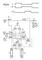
- FIG. 15 shows the switch arrangement S1 to S4 assigned to the recharging capacitor C1 (FIG. 2) and the logic circuit V1 connected to it.
- the switch arrangement shown in FIG. 15 has two transistors M7 and M8 which are connected in series and are connected to one another by their source connections. These two transistors form the changeover switch S1.
- the drain of transistor M7 is connected to VCC / 2 (which may be 0 V, for example).
- the drain connection of the transistor M8 is connected to the connection of the summing capacitor CI1 connected to the "- ⁇ input of the operational amplifier GTV.
- the charge-transfer capacitor C1 is connected to one of its connections at the connection point of the two transistors.
- the other connection of this charge-transfer capacitor is connected to the source connections of two transistors M5 and M6, these transistors forming the changeover switch S2, the connection point of a series circuit consisting of two transistors M1 and M2, forming the changeover switch S4, being connected to the drain connection of the transistor M5
- the source connection of the transistor M1 is connected to the "-" connection of the reference voltage source VREF, the "+” connection of which is connected to VCC / 2. 2 V.
- the transistor M2 is with its source connection connected to VCC / 2, for example 0 V.
- the aforementioned transistor M6 is connected to a connection point of a series circuit consisting of two transistors M3 and M4.
- the connection point is formed by the drain connections of these transistors.
- These transistors represent the changeover switch S3.
- the source connection of the transistor M3 is connected to VCC / 2 (0 V), the source connection of the transistor M4, on the other hand, is connected to the "-" connection of the reference voltage source already mentioned.
- an OR gate G1 is connected to the first register cell of shift register A and the fourteenth register cell of shift register B.
- the output of this OR gate is connected on the one hand to the gate terminal of transistor M5 and on the other hand to a first input of a NOR gate G3.
- the first register cell of shift register B and the fourteenth register cell of shift register A are connected to the two inputs of an OR gate G2.
- the output of this OR gate is connected on the one hand to the gate connection of the transistor M6 and on the other hand to the second input of the aforementioned NOR gate G3.
- the output of this NOR gate is connected to a first input of a further NOR gate G4.
- the second input of this NOR gate is with the clock phase of the 960 kHz clock signal shown in FIG. 15 is applied to the upper half.
- the output of the NOR gate G4 is connected to the gate terminal of the transistor M8.
- the transistors M1, M3 and M7 mentioned are each applied to the clock phase P2 at their gate connection.
- the transistors M2 and M4 on the other hand, each receive clock signals with the phase P1 at their gate connection, which, as can be seen from the clock signals indicated in FIG. 15, does not overlap with the phase P2.
- the OR gate G1 is used to select the states in which the recharging capacitor C1 is to cause a positive voltage jump at the output of the operational amplifier GTV. According to the table of values shown in FIG. 2 and the transmission pulse sequence shown in FIG. 3b, this is the case in the first period of a +1 transmission pulse and in the fourteenth period of a -1 transmission pulse. These periods are determined by the above-mentioned connection of the OR gate G1 with the shift registers A and B.
- transistor M5 is controlled in a conductive manner via the OR gate.
- the recharging capacitor C1 is then charged to the reference voltage VREF via the transistors M1, M5 and M7.
- transistors M2 and M8 are controlled to be conductive.
- the charge capacitor C1 is thus connected to 0 V (VCC / 2) with its two connections, and the charge flows to the summing capacitor CI1. This creates a positive voltage jump at the output of the operational amplifier GTV.
- transistor M6 is controlled to be conductive.
- the recharging capacitor C1 is discharged via the transistors M3, M6 and M7.
- the clock phase P1 or the transistors M4 and M8 are controlled to be conductive.
- the charge-reversal capacitor C1 thus lies between the summing capacitor CI1 and the reference voltage VREF and thus takes charge from the summing capacitor CI1. This causes a negative voltage jump at the output of the operational amplifier GTV.
- the logic circuit R indicated in FIGS. 2, 6, 9 and 12 and the logic additionally indicated in FIG. 6 circuit S each also contain only logic gates familiar to the person skilled in the art in order to control the times for the short-circuiting of the summing capacitors CI1 and CI2 or the closing of the switches SH and SH ⁇ on the basis of the samples passing through the shift registers A and B.
- pulse formers for the formation of three-level and four-level transmission pulses with symmetrical stepped edges.
- pulse formers described it is also possible to form transmission pulses with any step-shaped edges, that is to say, for example, with asymmetrical edges, by appropriately selecting the number of charge-transfer capacitors and the capacity of the charge-transfer capacitors.
- the pulse shapers described can also be designed for the formation of any multi-level transmission pulses by appropriate adaptation or expansion.
- a shift register arrangement A, B each provides control signals for the logic circuits connected to it.
- a device which can generally be referred to as a control signal generator, with a number of outputs corresponding to the number of register cells in the shift register arrangement A, B, which outputs control signals at their outputs in succession at equidistant time intervals on the occurrence of signals supplied to the respective pulse generator delivers.
- control signals are used to control the logic circuits present in the pulse shapers described.
- a clock generator may be mentioned here, for example, which is supplied with the signals supplied to the respective pulse generator.
Landscapes
- Engineering & Computer Science (AREA)
- Physics & Mathematics (AREA)
- Theoretical Computer Science (AREA)
- Computer Networks & Wireless Communication (AREA)
- Signal Processing (AREA)
- General Engineering & Computer Science (AREA)
- General Physics & Mathematics (AREA)
- Power Engineering (AREA)
- Spectroscopy & Molecular Physics (AREA)
- Analogue/Digital Conversion (AREA)
- Dc Digital Transmission (AREA)
Priority Applications (1)
| Application Number | Priority Date | Filing Date | Title |
|---|---|---|---|
| AT87113056T ATE87781T1 (de) | 1986-09-26 | 1987-09-07 | Impulsformer. |
Applications Claiming Priority (8)
| Application Number | Priority Date | Filing Date | Title |
|---|---|---|---|
| DE3632798 | 1986-09-26 | ||
| DE3632798 | 1986-09-26 | ||
| DE3714527 | 1987-04-30 | ||
| DE3714527 | 1987-04-30 | ||
| DE3722463 | 1987-07-07 | ||
| DE3722461 | 1987-07-07 | ||
| DE3722461 | 1987-07-07 | ||
| DE3722463 | 1987-07-07 |
Publications (3)
| Publication Number | Publication Date |
|---|---|
| EP0265637A2 true EP0265637A2 (fr) | 1988-05-04 |
| EP0265637A3 EP0265637A3 (en) | 1989-08-30 |
| EP0265637B1 EP0265637B1 (fr) | 1993-03-31 |
Family
ID=27433703
Family Applications (1)
| Application Number | Title | Priority Date | Filing Date |
|---|---|---|---|
| EP87113056A Expired - Lifetime EP0265637B1 (fr) | 1986-09-26 | 1987-09-07 | Circuit de mise en forme d'impulsion |
Country Status (8)
| Country | Link |
|---|---|
| EP (1) | EP0265637B1 (fr) |
| JP (1) | JPH0795329B2 (fr) |
| AU (1) | AU7897187A (fr) |
| CA (1) | CA1276690C (fr) |
| DE (1) | DE3785137D1 (fr) |
| DK (1) | DK499587A (fr) |
| FI (1) | FI874225A (fr) |
| NO (1) | NO874060L (fr) |
Cited By (2)
| Publication number | Priority date | Publication date | Assignee | Title |
|---|---|---|---|---|
| EP0564271A1 (fr) * | 1992-04-02 | 1993-10-06 | Sony Corporation | Générateur d'ondes |
| FR2706104A1 (fr) * | 1993-06-02 | 1994-12-09 | Klibanov Elvard | Système de transmission numérique utilisant un signal analogique composé des impulsions gaussiennes ou cos2 de polarités opposées. |
Families Citing this family (2)
| Publication number | Priority date | Publication date | Assignee | Title |
|---|---|---|---|---|
| JPH04150417A (ja) * | 1990-10-11 | 1992-05-22 | Matsushita Electric Ind Co Ltd | 変調装置 |
| US7079063B1 (en) * | 2005-04-18 | 2006-07-18 | Analog Devices, Inc. | System and method for tri-level logic data shuffling for oversampling data conversion |
-
1987
- 1987-09-07 EP EP87113056A patent/EP0265637B1/fr not_active Expired - Lifetime
- 1987-09-07 DE DE8787113056T patent/DE3785137D1/de not_active Expired - Lifetime
- 1987-09-23 DK DK499587A patent/DK499587A/da not_active Application Discontinuation
- 1987-09-24 CA CA000547734A patent/CA1276690C/fr not_active Expired - Fee Related
- 1987-09-25 FI FI874225A patent/FI874225A/fi not_active Application Discontinuation
- 1987-09-25 AU AU78971/87A patent/AU7897187A/en not_active Abandoned
- 1987-09-25 JP JP62239108A patent/JPH0795329B2/ja not_active Expired - Fee Related
- 1987-09-28 NO NO874060A patent/NO874060L/no unknown
Non-Patent Citations (4)
| Title |
|---|
| IEEE JOURNAL OF SOLID-STATE CIRCUITS, Band SC-19, Nr. 6, Dezember 1984, Seiten 861-869, IEEE, New York, US; C.A. LABER et al.: "A monolithic 1200 Baud FSK CMOS modem" * |
| IEEE TRANSACTIONS ON COMMUNICATION TECHNOLOGY, Band COM-16, Nr. 1, Februar 1968, Seiten 81-93, IEEE, New York, US; H.B. VOELCKER: "Generation of digital signaling waveforms" * |
| PROCEEDINGS 1982 INTERNATIONAL SYMPOSIUM ON SUBSCRIBER LOOPS AND SERVICES, Toronto, 20.-24. September 1982, Seiten 201-205, IEEE, New York, US; O. AGAZZI et al.: "Large scale integration of hybrid-method digital subscriber loops" * |
| PROCEEDINGS OF THE IEEE 1987 CUSTOM INTEGRATED CIRCUITS CONFERENCE, Portland, Oregon, 4.-7. Mai 1987, Seiten 457-460, IEEE, New York, US; B. ROESSLER et al.: "CMOS analog front end of a transceiver with digital echo cancellation for ISDN" * |
Cited By (2)
| Publication number | Priority date | Publication date | Assignee | Title |
|---|---|---|---|---|
| EP0564271A1 (fr) * | 1992-04-02 | 1993-10-06 | Sony Corporation | Générateur d'ondes |
| FR2706104A1 (fr) * | 1993-06-02 | 1994-12-09 | Klibanov Elvard | Système de transmission numérique utilisant un signal analogique composé des impulsions gaussiennes ou cos2 de polarités opposées. |
Also Published As
| Publication number | Publication date |
|---|---|
| DK499587A (da) | 1988-03-27 |
| EP0265637B1 (fr) | 1993-03-31 |
| CA1276690C (fr) | 1990-11-20 |
| DK499587D0 (da) | 1987-09-23 |
| NO874060D0 (no) | 1987-09-28 |
| FI874225A (fi) | 1988-03-27 |
| FI874225A0 (fi) | 1987-09-25 |
| NO874060L (no) | 1988-03-28 |
| AU7897187A (en) | 1988-03-31 |
| JPH01125682A (ja) | 1989-05-18 |
| JPH0795329B2 (ja) | 1995-10-11 |
| DE3785137D1 (de) | 1993-05-06 |
| EP0265637A3 (en) | 1989-08-30 |
Similar Documents
| Publication | Publication Date | Title |
|---|---|---|
| DE2842262C2 (de) | Gleichspannungswandler | |
| DE3044956A1 (de) | "digitaler hochleistungsverstaerker" | |
| DE3311067A1 (de) | Digital-analog-wandler hohen aufloesevermoegens | |
| DE3221305A1 (de) | Digital/analog-wandler | |
| EP0261482B1 (fr) | Amplificateur opérationnel | |
| EP0300560B1 (fr) | Circuit de comparison | |
| DE19601386C2 (de) | Ausgangspufferschaltkreis | |
| DE2836079A1 (de) | Digital-analog-umsetzer | |
| DE2801272A1 (de) | Schaltungsanordnung mit gewichtsfaktorabhaengiger ladungsaufteilung und -uebertragung | |
| EP0421395B2 (fr) | Agencement de conversion d'une grandeur électrique d'entrée en un signal électrique continu proportionnel à ladite grandeur | |
| EP0281001A2 (fr) | Agencement de circuit de conversion de valeurs de signal de ton numériques en signal de ton analogique | |
| DE3145889A1 (de) | Integrierbarer digital/analog-wandler | |
| DE2553694A1 (de) | Ladungsgekoppelter verstaerker | |
| DE1913641A1 (de) | Schaltmodulator | |
| DE1276736B (de) | Schaltung zur Verstaerkungssteuerung | |
| EP0265637B1 (fr) | Circuit de mise en forme d'impulsion | |
| DE2317584C3 (de) | Vorrichtung zur Umwandlung von numerischen Informationen in eine entsprechende, eine analoge Information darstellende Wechselspannung | |
| CH644233A5 (de) | Schaltungsanordnung zur umsetzung von digital-signalen, insbesondere pcm-signalen, in diesen entsprechende analog-signale, mit einem r-2r-kettennetzwerk. | |
| DE2337442A1 (de) | Verfahren und schaltungsanordnung zum kombinieren eines analogen signals mit einem digitalen signal | |
| DE2130701A1 (de) | Analog-Digital-Umsetzer | |
| DE1762829A1 (de) | Selbsteinstellender Analog-Digitalwandler | |
| DE3017463A1 (de) | Logische schaltungsanordnung mit asymmetrischen massenpunkt- bzw. quantum- interferenzschaltkreisen | |
| DE1487357A1 (de) | Modulatoren unter Verwendung von Feldeffekttransistoren | |
| DE2222182C2 (de) | Isolierter Digital-Analog-Wandler | |
| DE2803099C3 (de) | Digital-Analog-Umsetzer in integrierter Schaltungstechnik |
Legal Events
| Date | Code | Title | Description |
|---|---|---|---|
| PUAI | Public reference made under article 153(3) epc to a published international application that has entered the european phase |
Free format text: ORIGINAL CODE: 0009012 |
|
| AK | Designated contracting states |
Kind code of ref document: A2 Designated state(s): AT BE CH DE FR GB IT LI LU NL SE |
|
| PUAL | Search report despatched |
Free format text: ORIGINAL CODE: 0009013 |
|
| AK | Designated contracting states |
Kind code of ref document: A3 Designated state(s): AT BE CH DE FR GB IT LI LU NL SE |
|
| 17P | Request for examination filed |
Effective date: 19900226 |
|
| 17Q | First examination report despatched |
Effective date: 19920601 |
|
| GRAA | (expected) grant |
Free format text: ORIGINAL CODE: 0009210 |
|
| AK | Designated contracting states |
Kind code of ref document: B1 Designated state(s): AT BE CH DE FR GB IT LI LU NL SE |
|
| REF | Corresponds to: |
Ref document number: 87781 Country of ref document: AT Date of ref document: 19930415 Kind code of ref document: T |
|
| REF | Corresponds to: |
Ref document number: 3785137 Country of ref document: DE Date of ref document: 19930506 |
|
| ITF | It: translation for a ep patent filed |
Owner name: STUDIO JAUMANN |
|
| ET | Fr: translation filed | ||
| GBT | Gb: translation of ep patent filed (gb section 77(6)(a)/1977) |
Effective date: 19930610 |
|
| PG25 | Lapsed in a contracting state [announced via postgrant information from national office to epo] |
Ref country code: LU Free format text: LAPSE BECAUSE OF NON-PAYMENT OF DUE FEES Effective date: 19930930 |
|
| PLBE | No opposition filed within time limit |
Free format text: ORIGINAL CODE: 0009261 |
|
| STAA | Information on the status of an ep patent application or granted ep patent |
Free format text: STATUS: NO OPPOSITION FILED WITHIN TIME LIMIT |
|
| 26N | No opposition filed | ||
| PGFP | Annual fee paid to national office [announced via postgrant information from national office to epo] |
Ref country code: AT Payment date: 19940824 Year of fee payment: 8 |
|
| PGFP | Annual fee paid to national office [announced via postgrant information from national office to epo] |
Ref country code: CH Payment date: 19941216 Year of fee payment: 8 |
|
| EAL | Se: european patent in force in sweden |
Ref document number: 87113056.3 |
|
| PG25 | Lapsed in a contracting state [announced via postgrant information from national office to epo] |
Ref country code: AT Effective date: 19950907 |
|
| PG25 | Lapsed in a contracting state [announced via postgrant information from national office to epo] |
Ref country code: CH Effective date: 19950930 Ref country code: LI Effective date: 19950930 |
|
| REG | Reference to a national code |
Ref country code: CH Ref legal event code: PL |
|
| PGFP | Annual fee paid to national office [announced via postgrant information from national office to epo] |
Ref country code: BE Payment date: 19980909 Year of fee payment: 12 |
|
| PGFP | Annual fee paid to national office [announced via postgrant information from national office to epo] |
Ref country code: NL Payment date: 19980921 Year of fee payment: 12 |
|
| PG25 | Lapsed in a contracting state [announced via postgrant information from national office to epo] |
Ref country code: BE Free format text: LAPSE BECAUSE OF NON-PAYMENT OF DUE FEES Effective date: 19990930 |
|
| BERE | Be: lapsed |
Owner name: SIEMENS A.G. Effective date: 19990930 |
|
| PG25 | Lapsed in a contracting state [announced via postgrant information from national office to epo] |
Ref country code: NL Free format text: LAPSE BECAUSE OF NON-PAYMENT OF DUE FEES Effective date: 20000401 |
|
| NLV4 | Nl: lapsed or anulled due to non-payment of the annual fee |
Effective date: 20000401 |
|
| PGFP | Annual fee paid to national office [announced via postgrant information from national office to epo] |
Ref country code: SE Payment date: 20010913 Year of fee payment: 15 |
|
| REG | Reference to a national code |
Ref country code: GB Ref legal event code: IF02 |
|
| PG25 | Lapsed in a contracting state [announced via postgrant information from national office to epo] |
Ref country code: SE Free format text: LAPSE BECAUSE OF NON-PAYMENT OF DUE FEES Effective date: 20020908 |
|
| EUG | Se: european patent has lapsed | ||
| PGFP | Annual fee paid to national office [announced via postgrant information from national office to epo] |
Ref country code: FR Payment date: 20030904 Year of fee payment: 17 |
|
| PG25 | Lapsed in a contracting state [announced via postgrant information from national office to epo] |
Ref country code: FR Free format text: LAPSE BECAUSE OF NON-PAYMENT OF DUE FEES Effective date: 20050531 |
|
| REG | Reference to a national code |
Ref country code: FR Ref legal event code: ST |
|
| PG25 | Lapsed in a contracting state [announced via postgrant information from national office to epo] |
Ref country code: IT Free format text: LAPSE BECAUSE OF NON-PAYMENT OF DUE FEES;WARNING: LAPSES OF ITALIAN PATENTS WITH EFFECTIVE DATE BEFORE 2007 MAY HAVE OCCURRED AT ANY TIME BEFORE 2007. THE CORRECT EFFECTIVE DATE MAY BE DIFFERENT FROM THE ONE RECORDED. Effective date: 20050907 |
|
| PGFP | Annual fee paid to national office [announced via postgrant information from national office to epo] |
Ref country code: GB Payment date: 20060921 Year of fee payment: 20 |
|
| PGFP | Annual fee paid to national office [announced via postgrant information from national office to epo] |
Ref country code: DE Payment date: 20061114 Year of fee payment: 20 |
|
| REG | Reference to a national code |
Ref country code: GB Ref legal event code: PE20 |
|
| PG25 | Lapsed in a contracting state [announced via postgrant information from national office to epo] |
Ref country code: GB Free format text: LAPSE BECAUSE OF EXPIRATION OF PROTECTION Effective date: 20070906 |