EP0265320B1 - Dispositif de dépôt sous vide par pulvérisation cathodique réactive sur une feuille de verre - Google Patents
Dispositif de dépôt sous vide par pulvérisation cathodique réactive sur une feuille de verre Download PDFInfo
- Publication number
- EP0265320B1 EP0265320B1 EP87402242A EP87402242A EP0265320B1 EP 0265320 B1 EP0265320 B1 EP 0265320B1 EP 87402242 A EP87402242 A EP 87402242A EP 87402242 A EP87402242 A EP 87402242A EP 0265320 B1 EP0265320 B1 EP 0265320B1
- Authority
- EP
- European Patent Office
- Prior art keywords
- substrate
- diaphragms
- edges
- deposition chamber
- cathode
- Prior art date
- Legal status (The legal status is an assumption and is not a legal conclusion. Google has not performed a legal analysis and makes no representation as to the accuracy of the status listed.)
- Expired - Lifetime
Links
- 238000004544 sputter deposition Methods 0.000 title claims abstract description 8
- 238000001771 vacuum deposition Methods 0.000 title claims description 4
- 239000011521 glass Substances 0.000 title abstract description 19
- 238000000151 deposition Methods 0.000 claims abstract description 28
- 230000008021 deposition Effects 0.000 claims abstract description 25
- 238000000576 coating method Methods 0.000 claims abstract description 17
- 230000001681 protective effect Effects 0.000 claims abstract description 14
- 239000002245 particle Substances 0.000 claims abstract description 11
- 229910044991 metal oxide Inorganic materials 0.000 claims abstract description 6
- 150000004706 metal oxides Chemical class 0.000 claims abstract description 4
- 230000001154 acute effect Effects 0.000 claims abstract description 3
- 239000004065 semiconductor Substances 0.000 claims abstract description 3
- 150000002736 metal compounds Chemical class 0.000 claims abstract 2
- 239000000758 substrate Substances 0.000 claims description 18
- 239000011248 coating agent Substances 0.000 claims description 14
- 239000000463 material Substances 0.000 claims description 10
- 229910052751 metal Inorganic materials 0.000 claims description 10
- 239000002184 metal Substances 0.000 claims description 10
- 238000005520 cutting process Methods 0.000 claims description 7
- 239000010410 layer Substances 0.000 description 30
- 238000009434 installation Methods 0.000 description 11
- 239000012634 fragment Substances 0.000 description 6
- 230000003071 parasitic effect Effects 0.000 description 5
- XOLBLPGZBRYERU-UHFFFAOYSA-N tin dioxide Chemical compound O=[Sn]=O XOLBLPGZBRYERU-UHFFFAOYSA-N 0.000 description 4
- 238000004873 anchoring Methods 0.000 description 3
- 230000007547 defect Effects 0.000 description 3
- 230000000694 effects Effects 0.000 description 3
- 239000007789 gas Substances 0.000 description 3
- 230000002829 reductive effect Effects 0.000 description 3
- XKRFYHLGVUSROY-UHFFFAOYSA-N Argon Chemical compound [Ar] XKRFYHLGVUSROY-UHFFFAOYSA-N 0.000 description 2
- BQCADISMDOOEFD-UHFFFAOYSA-N Silver Chemical compound [Ag] BQCADISMDOOEFD-UHFFFAOYSA-N 0.000 description 2
- 238000000034 method Methods 0.000 description 2
- 239000011241 protective layer Substances 0.000 description 2
- 238000005546 reactive sputtering Methods 0.000 description 2
- 229910052709 silver Inorganic materials 0.000 description 2
- 239000004332 silver Substances 0.000 description 2
- RYGMFSIKBFXOCR-UHFFFAOYSA-N Copper Chemical compound [Cu] RYGMFSIKBFXOCR-UHFFFAOYSA-N 0.000 description 1
- 229910000831 Steel Inorganic materials 0.000 description 1
- UCKMPCXJQFINFW-UHFFFAOYSA-N Sulphide Chemical compound [S-2] UCKMPCXJQFINFW-UHFFFAOYSA-N 0.000 description 1
- 230000003667 anti-reflective effect Effects 0.000 description 1
- 229910052786 argon Inorganic materials 0.000 description 1
- 230000001174 ascending effect Effects 0.000 description 1
- QVGXLLKOCUKJST-UHFFFAOYSA-N atomic oxygen Chemical compound [O] QVGXLLKOCUKJST-UHFFFAOYSA-N 0.000 description 1
- 230000015572 biosynthetic process Effects 0.000 description 1
- 238000004140 cleaning Methods 0.000 description 1
- 150000001875 compounds Chemical class 0.000 description 1
- 239000000470 constituent Substances 0.000 description 1
- 238000010276 construction Methods 0.000 description 1
- 229910052802 copper Inorganic materials 0.000 description 1
- 239000010949 copper Substances 0.000 description 1
- 238000005336 cracking Methods 0.000 description 1
- 238000005137 deposition process Methods 0.000 description 1
- 230000001627 detrimental effect Effects 0.000 description 1
- 230000005684 electric field Effects 0.000 description 1
- 230000004907 flux Effects 0.000 description 1
- PCHJSUWPFVWCPO-UHFFFAOYSA-N gold Chemical compound [Au] PCHJSUWPFVWCPO-UHFFFAOYSA-N 0.000 description 1
- 229910052737 gold Inorganic materials 0.000 description 1
- 239000010931 gold Substances 0.000 description 1
- 230000000670 limiting effect Effects 0.000 description 1
- 238000001755 magnetron sputter deposition Methods 0.000 description 1
- 239000001301 oxygen Substances 0.000 description 1
- 229910052760 oxygen Inorganic materials 0.000 description 1
- 230000036961 partial effect Effects 0.000 description 1
- 230000005855 radiation Effects 0.000 description 1
- 230000000717 retained effect Effects 0.000 description 1
- 230000035939 shock Effects 0.000 description 1
- 239000005368 silicate glass Substances 0.000 description 1
- 238000005507 spraying Methods 0.000 description 1
- 230000000087 stabilizing effect Effects 0.000 description 1
- 239000010959 steel Substances 0.000 description 1
Images

Classifications
-
- C—CHEMISTRY; METALLURGY
- C23—COATING METALLIC MATERIAL; COATING MATERIAL WITH METALLIC MATERIAL; CHEMICAL SURFACE TREATMENT; DIFFUSION TREATMENT OF METALLIC MATERIAL; COATING BY VACUUM EVAPORATION, BY SPUTTERING, BY ION IMPLANTATION OR BY CHEMICAL VAPOUR DEPOSITION, IN GENERAL; INHIBITING CORROSION OF METALLIC MATERIAL OR INCRUSTATION IN GENERAL
- C23C—COATING METALLIC MATERIAL; COATING MATERIAL WITH METALLIC MATERIAL; SURFACE TREATMENT OF METALLIC MATERIAL BY DIFFUSION INTO THE SURFACE, BY CHEMICAL CONVERSION OR SUBSTITUTION; COATING BY VACUUM EVAPORATION, BY SPUTTERING, BY ION IMPLANTATION OR BY CHEMICAL VAPOUR DEPOSITION, IN GENERAL
- C23C14/00—Coating by vacuum evaporation, by sputtering or by ion implantation of the coating forming material
- C23C14/0021—Reactive sputtering or evaporation
- C23C14/0036—Reactive sputtering
-
- C—CHEMISTRY; METALLURGY
- C23—COATING METALLIC MATERIAL; COATING MATERIAL WITH METALLIC MATERIAL; CHEMICAL SURFACE TREATMENT; DIFFUSION TREATMENT OF METALLIC MATERIAL; COATING BY VACUUM EVAPORATION, BY SPUTTERING, BY ION IMPLANTATION OR BY CHEMICAL VAPOUR DEPOSITION, IN GENERAL; INHIBITING CORROSION OF METALLIC MATERIAL OR INCRUSTATION IN GENERAL
- C23C—COATING METALLIC MATERIAL; COATING MATERIAL WITH METALLIC MATERIAL; SURFACE TREATMENT OF METALLIC MATERIAL BY DIFFUSION INTO THE SURFACE, BY CHEMICAL CONVERSION OR SUBSTITUTION; COATING BY VACUUM EVAPORATION, BY SPUTTERING, BY ION IMPLANTATION OR BY CHEMICAL VAPOUR DEPOSITION, IN GENERAL
- C23C14/00—Coating by vacuum evaporation, by sputtering or by ion implantation of the coating forming material
- C23C14/22—Coating by vacuum evaporation, by sputtering or by ion implantation of the coating forming material characterised by the process of coating
- C23C14/56—Apparatus specially adapted for continuous coating; Arrangements for maintaining the vacuum, e.g. vacuum locks
- C23C14/564—Means for minimising impurities in the coating chamber such as dust, moisture, residual gases
Definitions
- the invention relates to a device for depositing under vacuum, in particular by reactive sputtering, on a transparent sheet substrate arranged in a horizontal position, a non-metallic layer consisting of a semiconductor, metallic oxide or another compound.
- metallic comprising a deposition chamber in which a vacuum can be established, a support or transport device for the substrate to be coated, at least one cathode disposed above the substrate and carrying the coating material, and electrodes and / or protective sheets and / or diaphragms arranged inside the deposition chamber.
- Devices of this type find particular application for coating sheets of glass or plastic with electrically conductive and / or heat reflecting layers.
- a metallic layer for example of gold, silver and / or copper, comprised between anchoring layers and / or layers of protection arranged respectively below and above this metal layer.
- the anchoring layers and / or the protective layers may comprise, for example, a metallic oxy or a metallic sulfide.
- a stack of layers which has provided good results for coating silicate glass sheets consists for example of a layer of tin dioxide forming an anchoring layer, a layer of silver forming a reflecting layer, d '' a thin protective layer of metal oxide and an anti-reflective layer of tin dioxide.
- Vacuum deposition devices of the type mentioned above work particularly economically when they operate on the principle of reactive sputtering assisted by a magnetic field.
- metallic targets are used as cathodes, and the sputtered metal is oxidized, during the reactive process, by means of oxygen added in small proportions to the gas introduced into the deposition chamber, thereby forming the desired layer of metal oxide on the substrate.
- Vacuum deposition devices operating on the sputtering principle are generally provided with additional accessories inserted between the cathode and the substrate to be coated. These additional accessories have different roles.
- the role of the electrodes designated under the term of anodes which are arranged symmetrically with respect to the cathodes and near the latter, consists in dispersing and stabilizing the plasma cloud.
- a positive electrical potential is applied to these anodes relative to the electrical potential of the cathode and relative to the potential of the metal case of the vacuum chamber.
- the anodes of the prior art have the form of circular profiles or tubes. In addition to the anodes and possibly also in place of the latter, it is also possible to have, above the substrate, protective sheets or diaphragms.
- these diaphragms consists first of all in limiting the flow of the particles reaching the upper surface of the substrate to the main radiation of the high energy sprayed particles, thus eliminating the lateral components of the particle beam, of significantly lower speed. .
- an electrical potential which may be equal for example to the ground potential of the housing of the deposition chamber, or else possibly be a positive potential with respect to this potential.
- such installations may also include protective sheets placed below the plane of the glass sheet, for example laterally, next to the substrate to be coated, so that these sheets protect the parts of the installation located above below, against a deposit of the pulverized material.
- the mechanical stresses increase, when the operating time increases, and the limit of mechanical resistance of the deposited layers can be exceeded.
- fragments of the deposited layers can then detach from the support and fall, or jump, through the opening of the diaphragms and fail on the surface of the substrate.
- defects appear in the coating formed on the substrate.
- the deposition process must be interrupted at regular intervals in order to remove deposits on the components affected by such layers of fragile deposits or else replace the components bearing such deposits with components having undergone cleaning.
- the object of the invention is to reduce or preferably eliminate the defects due to the detachment of deposits of the coating material on the electrodes, diaphragms, protective sheets or other components capable of being placed inside the chamber for depositing vacuum spraying installations, and to extend the periods of continuous operation of such installations, thereby improving their profitability.
- these objectives are achieved if the elements or surfaces liable to be exposed to the flow of particles emitted by the cathode, electrodes and / or other components of the device located inside the chamber deposit are provided with edges and / or projecting parts, in the form of a sharp edge, that is to say comprising surfaces forming between them an acute angle, said elements not exposing said flow, near the edges looking at the substrate to be coated, no surface inclined downward towards said edges.
- the arrangements in accordance with the invention make it possible to achieve, surprisingly, that the risk of detachment or ejection of fragments from the deposits formed is greatly reduced.
- This effect clearly results from the fact that the mechanical stresses, which appear at inside the deposit and / or between the deposit and the metallic support, are reduced or even eliminated when the deposit layers crack in a linear geometry along the sharp edges or sharp projecting parts, without the layers also lose their cohesion.
- the deposition layers partially detach from their support during cracking along these "imposed rupture zones, but large surface fragments are formed which still adhere at least in places to the support. which have cracked and have risen or partially detached from the support are then partially retained thanks to subsequent deposits.
- the edges of the diaphragms consisting of plates are in the form of a sharp tapered blade, the underside of which, in a bevel and substantially planar, makes an angle alpha less than or equal to 45 degrees from the top.
- the front bevelled face of these components is turned over its entire width opposite the cathode and the flux. particles, so that the possibility of deposit layers on this surface is greatly reduced.
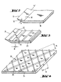
- FIG. 1 represents a deposition chamber of a sputtering installation operating continuously and serving to produce the coating of glass sheets, provided with its most important components, according to a perspective view represented in partial section .
- FIG. 2 represents a modified embodiment of the edge of a diaphragm produced in accordance with the invention, according to a view on a larger scale.
- FIG. 3 represents a possible embodiment of a surface of a diaphragm, produced in accordance with the invention.
- FIG. 4 represents another embodiment of a surface configuration, in accordance with the invention, of a protective sheet or of another component exposed to the flow of particles in a deposition chamber.
- FIG 1 the basic structure of a deposition chamber inside a sputtering plant operating continuously for glass sheets, provided with its essential constituent elements.
- the installation consists of a vacuum-tight channel-shaped housing 1, of a stable mechanical structure, through which the glass sheets 2 intended to receive the coating are moved on a transport path comprising transport rollers 3
- chambers forming an airlock are provided, which serve respectively to introduce the glass plates intended to receive their coating in the installation placed under high vacuum, or to extract them therefrom. that they have been coated.
- the installation area where the coating is practically carried out comprises several deposition chambers arranged one behind the other, for example four deposition chambers when it is planned to deposit a stack of layers comprising four layers. Each deposit chamber has the same basic structure.
- an elongate cathode 4 which extends over the entire width of the installation or at least over the width of the glass sheets intended to be coated, is arranged opposite the transport rollers 3 and parallel to these latter.
- the target 5 On the underside of the cathode 4 is fixed the target 5, which consists of the material to be deposited on the substrate by means of sputtering.
- a negative voltage is applied to the cathode 4 or to the target 5 while the housing 1 is placed at ground potential. Thanks to tubular pipes, not shown, small quantities of gas, for example argon, are introduced into the deposition chamber.
- the gas molecules are ionized in the electric field, and strike at high speed the surface of the target 5 from which, under the effect of shocks, they eject metallic atoms constituting a cloud of plasma in the form of negatively charged particles which are accelerated towards parts placed at ground potential or at positive potential. These particles accumulate on the surface of the substrate and on other surfaces subjected to the action of the plasma cloud, inside the deposition chamber.
- the deposition rate is greatly increased by the use of an intense magnetic field below the cathode, by means of strong permanent magnets placed in the cathode.
- the magnet device has not been shown in the drawings.
- tubular anode bodies 8 parallel and symmetrical with respect to the cathode 4, anodes to which a positive electrical potential is applied.
- protective plates or diaphragms 10 disposed below these anode bodies 8 and at a short distance above the glass sheet 2, are fixed to the vertical walls 11 delimiting the deposition chamber. The role of these diaphragms 10 is to collect the lateral components of the flow of particles and to let pass only the main flow which strikes the surface of the substrate under a substantially perpendicular incidence and with high energy.
- the diaphragms 10 are generally placed at ground potential.
- the coating material is deposited on the anode bodies 8 and the diaphragms 10 as well as on the glass sheet, and this precisely on the part of their surface facing the cathode.
- the coating material is deposited on the ends 12 ′, in their part not protected by the glass sheet 2, protective plates 12 arranged between the transport rollers 3 below said glass sheet.
- the protective plates 12 are arranged below the plane of the glass sheet 2, the parasitic deposits which form in these places can however project fragments likely to reach the surface of the glass sheet during fractures of the glass. coating under the effect of the stresses affecting these deposits.
- the diaphragms 10 are constituted by sheet metal plates having a thickness of a few millimeters.
- the edges, or edges of these diaphragms 10 constitute critical zones from the point of view of the coating material deposition operation, due to the detachment of these parasitic deposits.
- the zone of the edge 10 ′ is tapered in the form of a sharp blade, and the angle alpha formed by the faces of the edge of the diaphragms must be equal to or less than 45 degrees.
- the cutting edge wire 13 is situated at a level at least equal to that of the rest of the active part, exposed to parasitic deposits, of the upper face of the body of the diaphragm 10, so that only the lower face of said body has an oblique portion 14 looking at the glass sheet to be coated.
- the aim is thus to avoid, on the upper face 15 of the diaphragm, any surface inclined downward towards and near the edge of the diaphragm, which would facilitate falling onto the sheet of glass. fragments of the parasitic deposit.
- FIG. 2 An embodiment, constituting an improvement playing in the direction indicated last, is shown in FIG. 2 for the configuration of the zone of the edge 16 ′ of a diaphragm 16.
- the edge of the diaphragm presents at again a tapered edge 17, formed by the upper inclined face 18 and by the lower inclined face 19, these two inclined faces 18, 19 again making an alpha angle equal to or preferably less than 45 degrees, and said upper inclined face 18 having an ascending slope towards the cutting edge 17, so that the fragments of a deposit layer possibly released on the inclined face 18 tend to move in the opposite direction, on the slope of this inclined face, and to remain on the diaphragm body.
- the upper surface of the diaphragm body 20 has several prismatic protrusions 22, which extend parallel to the tapered edge 21 and themselves have tapered edges.
- the prismatic protrusions 22 have a height H of between 2 and 10 mm and preferably between 4 and 6 mm, and their base surface has a width B of between 2 and 4 mm, the angle formed by the faces of the premiums at the edge of a sharp shape being in all cases less than 45 degrees.
- the surfaces subject to a risk of parasitic deposition for example the upper face of a protective sheet 24, can also be provided with a grid 25 in the form of a network formed by prismatic bodies. projections 26 in the form of blades.
- the prismatic bodies 26 can have the same dimensions in cross section as the prismatic bodies 22 in FIG. 3.
- the distance A between the prismatic bodies 26 can vary within wide limits; good results are obtained when the distance A is between 5 and 25 mm and preferably between 10 and 15 mm.
- the prismatic projecting parts 22 or the grids 25 in the form of networks be made in one piece with their respective support. Furthermore, the desired goal is also achieved when the prismatic bodies or grids in the form of networks are produced in the form of elements distinct from their respective support.
- grids 25 in the form of networks there are thus suitable for example also particular embodiments of expanded metal panels available on the market, which consist of a rigid mesh network which is obtained by cutting and subsequent drawing of sheet metal sheets. of steel.
Landscapes
- Chemical & Material Sciences (AREA)
- Organic Chemistry (AREA)
- Engineering & Computer Science (AREA)
- Materials Engineering (AREA)
- Mechanical Engineering (AREA)
- Metallurgy (AREA)
- Chemical Kinetics & Catalysis (AREA)
- Physical Vapour Deposition (AREA)
- Blinds (AREA)
- Photovoltaic Devices (AREA)
- Breeding Of Plants And Reproduction By Means Of Culturing (AREA)
- Supports For Plants (AREA)
- Window Of Vehicle (AREA)
- Surface Treatment Of Glass (AREA)
Priority Applications (1)
| Application Number | Priority Date | Filing Date | Title |
|---|---|---|---|
| AT87402242T ATE66966T1 (de) | 1986-10-11 | 1987-10-08 | Anlage zur vakuum-auflagerung durch reaktive kathodenzerstaeubung auf eine glasplatte. |
Applications Claiming Priority (2)
| Application Number | Priority Date | Filing Date | Title |
|---|---|---|---|
| DE3634710 | 1986-10-11 | ||
| DE19863634710 DE3634710A1 (de) | 1986-10-11 | 1986-10-11 | Vorrichtung zum vakuumbeschichten einer glasscheibe durch reaktive kathodenzerstaeubung |
Publications (2)
| Publication Number | Publication Date |
|---|---|
| EP0265320A1 EP0265320A1 (fr) | 1988-04-27 |
| EP0265320B1 true EP0265320B1 (fr) | 1991-09-04 |
Family
ID=6311558
Family Applications (1)
| Application Number | Title | Priority Date | Filing Date |
|---|---|---|---|
| EP87402242A Expired - Lifetime EP0265320B1 (fr) | 1986-10-11 | 1987-10-08 | Dispositif de dépôt sous vide par pulvérisation cathodique réactive sur une feuille de verre |
Country Status (7)
| Country | Link |
|---|---|
| US (1) | US5080774A (enExample) |
| EP (1) | EP0265320B1 (enExample) |
| JP (1) | JPS63105963A (enExample) |
| AT (1) | ATE66966T1 (enExample) |
| DE (2) | DE3634710A1 (enExample) |
| ES (1) | ES2026558T3 (enExample) |
| FI (1) | FI82717C (enExample) |
Families Citing this family (19)
| Publication number | Priority date | Publication date | Assignee | Title |
|---|---|---|---|---|
| JPH01152271A (ja) * | 1987-12-09 | 1989-06-14 | Toshiba Corp | スパッタ装置 |
| FR2698093B1 (fr) * | 1992-11-17 | 1995-01-27 | Saint Gobain Vitrage Int | Vitrage à propriétés de transmission variant avec l'incidence. |
| KR970009828B1 (en) * | 1994-02-23 | 1997-06-18 | Sansung Electronics Co Ltd | Fabrication method of collimator |
| US5614071A (en) * | 1995-06-28 | 1997-03-25 | Hmt Technology Corporation | Sputtering shield |
| JP2001509214A (ja) * | 1997-01-16 | 2001-07-10 | ボトムフィールド,ロジャー,エル. | 蒸気蒸着構成要素及び対応する方法 |
| JP2002105628A (ja) * | 2000-10-03 | 2002-04-10 | Nissin Electric Co Ltd | 真空アーク蒸着装置 |
| DE10132478C1 (de) * | 2001-07-03 | 2003-04-30 | Atotech Deutschland Gmbh | Verfahren zum Abscheiden einer Metallschicht sowie Verfahren zum Regenerieren einer Metallionen in einer hohen Oxidationsstufe enthaltenden Lösung |
| US6495000B1 (en) * | 2001-07-16 | 2002-12-17 | Sharp Laboratories Of America, Inc. | System and method for DC sputtering oxide films with a finned anode |
| US8500965B2 (en) * | 2004-05-06 | 2013-08-06 | Ppg Industries Ohio, Inc. | MSVD coating process |
| KR101165466B1 (ko) * | 2005-08-31 | 2012-07-13 | 엘지디스플레이 주식회사 | 캐리어 및 이를 구비한 공정 장치 |
| US8603250B2 (en) * | 2006-06-27 | 2013-12-10 | First Solar, Inc. | System and method for deposition of a material on a substrate |
| US20080017501A1 (en) * | 2006-07-21 | 2008-01-24 | Makoto Inagawa | Cooled dark space shield for multi-cathode design |
| US20090194414A1 (en) * | 2008-01-31 | 2009-08-06 | Nolander Ira G | Modified sputtering target and deposition components, methods of production and uses thereof |
| EP2354271A1 (en) * | 2010-02-09 | 2011-08-10 | Applied Materials, Inc. | Substrate protection device and method |
| DE102010052761A1 (de) * | 2010-11-30 | 2012-05-31 | Leybold Optics Gmbh | Vorrichtung zum Beschichten eines Substrats |
| KR20140047276A (ko) * | 2012-10-12 | 2014-04-22 | 삼성디스플레이 주식회사 | 스퍼터링 장치 |
| CN106756780B (zh) * | 2017-01-23 | 2019-03-05 | 京东方科技集团股份有限公司 | 一种用于溅射成膜工艺的掩膜板及溅射装置 |
| CH715877A1 (de) * | 2019-02-26 | 2020-08-31 | Oerlikon Surface Solutions Ag Pfaeffikon | Vakuumkammer mit Elektrodenanordnung für eine Plasmaquelle zur Durchführung von Plasmabehandlungen. |
| DE102022103180A1 (de) | 2022-02-10 | 2023-08-10 | Voestalpine Stahl Gmbh | Verfahren zum Erzeugen von beschichtetem perforiertem Stahlband |
Family Cites Families (10)
| Publication number | Priority date | Publication date | Assignee | Title |
|---|---|---|---|---|
| US3514391A (en) * | 1967-05-05 | 1970-05-26 | Nat Res Corp | Sputtering apparatus with finned anode |
| US4094763A (en) * | 1970-07-31 | 1978-06-13 | Ppg Industries, Inc. | Sputter coating of glass with an oxide of a metal having an atomic number between 48 and 51 and mixtures thereof |
| US3945911A (en) * | 1974-08-28 | 1976-03-23 | Shatterproof Glass Corporation | Cathodes for sputter-coating glass sheets or other substrates |
| US4100055A (en) * | 1977-06-10 | 1978-07-11 | Varian Associates, Inc. | Target profile for sputtering apparatus |
| US4313815A (en) * | 1978-04-07 | 1982-02-02 | Varian Associates, Inc. | Sputter-coating system, and vaccuum valve, transport, and sputter source array arrangements therefor |
| DD140481A1 (de) * | 1978-11-20 | 1980-03-05 | Juergen Salm | Verfahren und vorrichtung zum aufbringen von isolatorschichten |
| NL8202092A (nl) * | 1982-05-21 | 1983-12-16 | Philips Nv | Magnetronkathodesputtersysteem. |
| US4545882A (en) * | 1983-09-02 | 1985-10-08 | Shatterproof Glass Corporation | Method and apparatus for detecting sputtering target depletion |
| DE3331707A1 (de) * | 1983-09-02 | 1985-03-21 | Leybold-Heraeus GmbH, 5000 Köln | Verfahren und vorrichtung zum reaktiven aufstaeuben von verbindungen von metallen und halbleitern |
| GB2194965B (en) * | 1986-09-12 | 1991-01-09 | Sharp Kk | A process for preparing a soft magnetic film of ni-fe based alloy |
-
1986
- 1986-10-11 DE DE19863634710 patent/DE3634710A1/de active Granted
-
1987
- 1987-10-08 ES ES198787402242T patent/ES2026558T3/es not_active Expired - Lifetime
- 1987-10-08 AT AT87402242T patent/ATE66966T1/de not_active IP Right Cessation
- 1987-10-08 DE DE8787402242T patent/DE3772706D1/de not_active Expired - Fee Related
- 1987-10-08 EP EP87402242A patent/EP0265320B1/fr not_active Expired - Lifetime
- 1987-10-09 FI FI874464A patent/FI82717C/fi not_active IP Right Cessation
- 1987-10-09 JP JP62253939A patent/JPS63105963A/ja active Pending
-
1990
- 1990-02-08 US US07/477,160 patent/US5080774A/en not_active Expired - Fee Related
Also Published As
| Publication number | Publication date |
|---|---|
| FI82717B (fi) | 1990-12-31 |
| DE3772706D1 (de) | 1991-10-10 |
| US5080774A (en) | 1992-01-14 |
| FI874464L (fi) | 1988-04-12 |
| DE3634710C2 (enExample) | 1989-01-12 |
| ATE66966T1 (de) | 1991-09-15 |
| FI82717C (fi) | 1991-04-10 |
| JPS63105963A (ja) | 1988-05-11 |
| DE3634710A1 (de) | 1988-04-21 |
| ES2026558T3 (es) | 1992-05-01 |
| EP0265320A1 (fr) | 1988-04-27 |
| FI874464A0 (fi) | 1987-10-09 |
Similar Documents
| Publication | Publication Date | Title |
|---|---|---|
| EP0265320B1 (fr) | Dispositif de dépôt sous vide par pulvérisation cathodique réactive sur une feuille de verre | |
| FR2490399A1 (fr) | Procede et appareil pour la pulverisation ou vaporisation utilisant une source d'ions amelioree | |
| FR2568269A1 (fr) | Dispositif de pulverisation pour installations de pulverisation cathodique | |
| EP1307607A1 (fr) | Procede et dispositif pour traiter des substrats metalliques au defile par plasma | |
| FR2500852A1 (enExample) | ||
| WO2005000758A2 (fr) | Substrat revetu d’une couche dielectrique et procede et installation pour sa fabrication | |
| BE1010420A3 (fr) | Procede pour la formation d'un revetement sur un substrat et installation pour la mise en oeuvre de ce procede. | |
| FR2517332A1 (fr) | Procede et ecran d'arret perfectionnes pour definir le profil d'epaisseur de couches deposees par pulverisation sur un substrat semi-conducteur | |
| FR2600269A1 (fr) | Procede et agencement pour pulveriser une matiere par decharge a haute frequence | |
| EP0413617B1 (fr) | Procédé de dépôt de couches minces | |
| WO2009053235A1 (fr) | Procede et dispositif pour le traitement par plasma de substrats au defile | |
| EP0674804B1 (fr) | Installation de depot d'un materiau metallique sur une plaque par evaporation | |
| FR2490873A1 (fr) | Procede et dispositif destines a produire une neutralisation amelioree d'un faisceau d'ions positifs | |
| EP0241447B1 (fr) | Cathode de pulvérisation | |
| BE1011098A3 (fr) | Procede et dispositif de decapage. | |
| EP0703599B1 (fr) | Cathode rotative de pulvérisation cathodique à plusieurs cibles | |
| WO2008080835A2 (fr) | Formation de couches par magnetron | |
| BE1004442A3 (fr) | Installation de pulverisation cathodique a taux eleve. | |
| EP0908924B1 (fr) | Dispositif pour la formation d'un revêtement sur un substrat par condensation | |
| EP2365513B1 (fr) | Enveloppe de protection pour canon à ions, dispositif de dépôt de matériaux par évaporation sous vide comprenant une telle enveloppe de protection et procédé de dépôt de matériaux | |
| FR2646287A1 (fr) | Barriere de correction magnetique pour canons a electrons | |
| EP3368704B1 (fr) | Dispositif pour la fabrication d'une couche en carbone amorphe par plasma a la resonance cyclotron electronique | |
| US20240191341A1 (en) | Stable ground anode aperture for thin film processing | |
| FR2663042A1 (fr) | Procede de realisation d'un revetement de haute adherence sur un support et notamment sur une tole d'acier, et produit ainsi obtenu. | |
| EP0454584A1 (fr) | Procédé et dispositif de dÀ©contamination par décapage ionique |
Legal Events
| Date | Code | Title | Description |
|---|---|---|---|
| PUAI | Public reference made under article 153(3) epc to a published international application that has entered the european phase |
Free format text: ORIGINAL CODE: 0009012 |
|
| AK | Designated contracting states |
Kind code of ref document: A1 Designated state(s): AT BE CH DE ES FR GB IT LI LU NL SE |
|
| 17P | Request for examination filed |
Effective date: 19881008 |
|
| RAP1 | Party data changed (applicant data changed or rights of an application transferred) |
Owner name: VEGLA VEREINIGTE GLASWERKE GMBH Owner name: SAINT-GOBAIN VITRAGE INTERNATIONAL |
|
| 17Q | First examination report despatched |
Effective date: 19900322 |
|
| GRAA | (expected) grant |
Free format text: ORIGINAL CODE: 0009210 |
|
| AK | Designated contracting states |
Kind code of ref document: B1 Designated state(s): AT BE CH DE ES FR GB IT LI LU NL SE |
|
| REF | Corresponds to: |
Ref document number: 66966 Country of ref document: AT Date of ref document: 19910915 Kind code of ref document: T |
|
| REF | Corresponds to: |
Ref document number: 3772706 Country of ref document: DE Date of ref document: 19911010 |
|
| ITF | It: translation for a ep patent filed | ||
| GBT | Gb: translation of ep patent filed (gb section 77(6)(a)/1977) | ||
| RAP2 | Party data changed (patent owner data changed or rights of a patent transferred) |
Owner name: VEGLA VEREINIGTE GLASWERKE GMBH Owner name: SAINT-GOBAIN VITRAGE INTERNATIONAL |
|
| REG | Reference to a national code |
Ref country code: CH Ref legal event code: PUE Owner name: SAINT-GOBAIN VITRAGE INTERNATIONAL |
|
| K2C1 | Correction of patent specification (title page) published |
Effective date: 19910904 |
|
| NLXE | Nl: other communications concerning ep-patents (part 3 heading xe) |
Free format text: IN PAT.BUL.01/92,PAGES 100 AND 127:CORR.:SAINT-GOBAIN VITRAGE INTERNATIONAL |
|
| REG | Reference to a national code |
Ref country code: ES Ref legal event code: FG2A Ref document number: 2026558 Country of ref document: ES Kind code of ref document: T3 |
|
| PLBE | No opposition filed within time limit |
Free format text: ORIGINAL CODE: 0009261 |
|
| STAA | Information on the status of an ep patent application or granted ep patent |
Free format text: STATUS: NO OPPOSITION FILED WITHIN TIME LIMIT |
|
| 26N | No opposition filed | ||
| EPTA | Lu: last paid annual fee | ||
| EAL | Se: european patent in force in sweden |
Ref document number: 87402242.9 |
|
| PGFP | Annual fee paid to national office [announced via postgrant information from national office to epo] |
Ref country code: SE Payment date: 19960909 Year of fee payment: 10 |
|
| PGFP | Annual fee paid to national office [announced via postgrant information from national office to epo] |
Ref country code: GB Payment date: 19960925 Year of fee payment: 10 |
|
| PGFP | Annual fee paid to national office [announced via postgrant information from national office to epo] |
Ref country code: AT Payment date: 19961009 Year of fee payment: 10 |
|
| PGFP | Annual fee paid to national office [announced via postgrant information from national office to epo] |
Ref country code: ES Payment date: 19961016 Year of fee payment: 10 |
|
| PGFP | Annual fee paid to national office [announced via postgrant information from national office to epo] |
Ref country code: FR Payment date: 19961017 Year of fee payment: 10 |
|
| PGFP | Annual fee paid to national office [announced via postgrant information from national office to epo] |
Ref country code: NL Payment date: 19961031 Year of fee payment: 10 |
|
| PG25 | Lapsed in a contracting state [announced via postgrant information from national office to epo] |
Ref country code: GB Free format text: LAPSE BECAUSE OF NON-PAYMENT OF DUE FEES Effective date: 19971008 Ref country code: AT Free format text: LAPSE BECAUSE OF NON-PAYMENT OF DUE FEES Effective date: 19971008 |
|
| PG25 | Lapsed in a contracting state [announced via postgrant information from national office to epo] |
Ref country code: SE Free format text: LAPSE BECAUSE OF NON-PAYMENT OF DUE FEES Effective date: 19971009 Ref country code: ES Free format text: LAPSE BECAUSE OF NON-PAYMENT OF DUE FEES Effective date: 19971009 |
|
| PG25 | Lapsed in a contracting state [announced via postgrant information from national office to epo] |
Ref country code: FR Free format text: THE PATENT HAS BEEN ANNULLED BY A DECISION OF A NATIONAL AUTHORITY Effective date: 19971031 |
|
| PG25 | Lapsed in a contracting state [announced via postgrant information from national office to epo] |
Ref country code: NL Free format text: LAPSE BECAUSE OF NON-PAYMENT OF DUE FEES Effective date: 19980501 |
|
| GBPC | Gb: european patent ceased through non-payment of renewal fee |
Effective date: 19971008 |
|
| NLV4 | Nl: lapsed or anulled due to non-payment of the annual fee |
Effective date: 19980501 |
|
| EUG | Se: european patent has lapsed |
Ref document number: 87402242.9 |
|
| REG | Reference to a national code |
Ref country code: FR Ref legal event code: ST |
|
| PGFP | Annual fee paid to national office [announced via postgrant information from national office to epo] |
Ref country code: BE Payment date: 19981029 Year of fee payment: 12 |
|
| PGFP | Annual fee paid to national office [announced via postgrant information from national office to epo] |
Ref country code: LU Payment date: 19981104 Year of fee payment: 12 |
|
| PGFP | Annual fee paid to national office [announced via postgrant information from national office to epo] |
Ref country code: DE Payment date: 19981114 Year of fee payment: 12 |
|
| PGFP | Annual fee paid to national office [announced via postgrant information from national office to epo] |
Ref country code: CH Payment date: 19990125 Year of fee payment: 12 |
|
| PG25 | Lapsed in a contracting state [announced via postgrant information from national office to epo] |
Ref country code: LU Free format text: LAPSE BECAUSE OF NON-PAYMENT OF DUE FEES Effective date: 19991008 |
|
| PG25 | Lapsed in a contracting state [announced via postgrant information from national office to epo] |
Ref country code: LI Free format text: LAPSE BECAUSE OF NON-PAYMENT OF DUE FEES Effective date: 19991031 Ref country code: CH Free format text: LAPSE BECAUSE OF NON-PAYMENT OF DUE FEES Effective date: 19991031 Ref country code: BE Free format text: LAPSE BECAUSE OF NON-PAYMENT OF DUE FEES Effective date: 19991031 |
|
| BERE | Be: lapsed |
Owner name: VEGLA VEREINIGTE GLASWERKE G.M.B.H. Effective date: 19991031 Owner name: SAINT-GOBAIN VITRAGE INTERNATIONAL Effective date: 19991031 |
|
| REG | Reference to a national code |
Ref country code: CH Ref legal event code: PL |
|
| PG25 | Lapsed in a contracting state [announced via postgrant information from national office to epo] |
Ref country code: DE Free format text: LAPSE BECAUSE OF NON-PAYMENT OF DUE FEES Effective date: 20000801 |
|
| REG | Reference to a national code |
Ref country code: ES Ref legal event code: FD2A Effective date: 19981113 |
|
| PG25 | Lapsed in a contracting state [announced via postgrant information from national office to epo] |
Ref country code: IT Free format text: LAPSE BECAUSE OF NON-PAYMENT OF DUE FEES;WARNING: LAPSES OF ITALIAN PATENTS WITH EFFECTIVE DATE BEFORE 2007 MAY HAVE OCCURRED AT ANY TIME BEFORE 2007. THE CORRECT EFFECTIVE DATE MAY BE DIFFERENT FROM THE ONE RECORDED. Effective date: 20051008 |