EP0264858A2 - Dynamische RAM-Zelle mit einem gemeinsamen Grabenspeicherkondensator, welcher durch die Seitenwände definierte Brückenkontakte und Torelektroden aufweist - Google Patents
Dynamische RAM-Zelle mit einem gemeinsamen Grabenspeicherkondensator, welcher durch die Seitenwände definierte Brückenkontakte und Torelektroden aufweist Download PDFInfo
- Publication number
- EP0264858A2 EP0264858A2 EP87115186A EP87115186A EP0264858A2 EP 0264858 A2 EP0264858 A2 EP 0264858A2 EP 87115186 A EP87115186 A EP 87115186A EP 87115186 A EP87115186 A EP 87115186A EP 0264858 A2 EP0264858 A2 EP 0264858A2
- Authority
- EP
- European Patent Office
- Prior art keywords
- layer
- trench
- substrate
- polysilicon
- forming
- Prior art date
- Legal status (The legal status is an assumption and is not a legal conclusion. Google has not performed a legal analysis and makes no representation as to the accuracy of the status listed.)
- Granted
Links
Images
Classifications
-
- H—ELECTRICITY
- H10—SEMICONDUCTOR DEVICES; ELECTRIC SOLID-STATE DEVICES NOT OTHERWISE PROVIDED FOR
- H10B—ELECTRONIC MEMORY DEVICES
- H10B12/00—Dynamic random access memory [DRAM] devices
- H10B12/01—Manufacture or treatment
- H10B12/02—Manufacture or treatment for one transistor one-capacitor [1T-1C] memory cells
- H10B12/03—Making the capacitor or connections thereto
- H10B12/038—Making the capacitor or connections thereto the capacitor being in a trench in the substrate
-
- H—ELECTRICITY
- H01—ELECTRIC ELEMENTS
- H01L—SEMICONDUCTOR DEVICES NOT COVERED BY CLASS H10
- H01L21/00—Processes or apparatus adapted for the manufacture or treatment of semiconductor or solid state devices or of parts thereof
- H01L21/02—Manufacture or treatment of semiconductor devices or of parts thereof
- H01L21/04—Manufacture or treatment of semiconductor devices or of parts thereof the devices having at least one potential-jump barrier or surface barrier, e.g. PN junction, depletion layer or carrier concentration layer
- H01L21/18—Manufacture or treatment of semiconductor devices or of parts thereof the devices having at least one potential-jump barrier or surface barrier, e.g. PN junction, depletion layer or carrier concentration layer the devices having semiconductor bodies comprising elements of Group IV of the Periodic System or AIIIBV compounds with or without impurities, e.g. doping materials
- H01L21/28—Manufacture of electrodes on semiconductor bodies using processes or apparatus not provided for in groups H01L21/20 - H01L21/268
- H01L21/283—Deposition of conductive or insulating materials for electrodes conducting electric current
- H01L21/285—Deposition of conductive or insulating materials for electrodes conducting electric current from a gas or vapour, e.g. condensation
- H01L21/28506—Deposition of conductive or insulating materials for electrodes conducting electric current from a gas or vapour, e.g. condensation of conductive layers
- H01L21/28512—Deposition of conductive or insulating materials for electrodes conducting electric current from a gas or vapour, e.g. condensation of conductive layers on semiconductor bodies comprising elements of Group IV of the Periodic System
- H01L21/28525—Deposition of conductive or insulating materials for electrodes conducting electric current from a gas or vapour, e.g. condensation of conductive layers on semiconductor bodies comprising elements of Group IV of the Periodic System the conductive layers comprising semiconducting material
-
- H—ELECTRICITY
- H10—SEMICONDUCTOR DEVICES; ELECTRIC SOLID-STATE DEVICES NOT OTHERWISE PROVIDED FOR
- H10B—ELECTRONIC MEMORY DEVICES
- H10B12/00—Dynamic random access memory [DRAM] devices
- H10B12/30—DRAM devices comprising one-transistor - one-capacitor [1T-1C] memory cells
- H10B12/37—DRAM devices comprising one-transistor - one-capacitor [1T-1C] memory cells the capacitor being at least partially in a trench in the substrate
-
- Y—GENERAL TAGGING OF NEW TECHNOLOGICAL DEVELOPMENTS; GENERAL TAGGING OF CROSS-SECTIONAL TECHNOLOGIES SPANNING OVER SEVERAL SECTIONS OF THE IPC; TECHNICAL SUBJECTS COVERED BY FORMER USPC CROSS-REFERENCE ART COLLECTIONS [XRACs] AND DIGESTS
- Y10—TECHNICAL SUBJECTS COVERED BY FORMER USPC
- Y10S—TECHNICAL SUBJECTS COVERED BY FORMER USPC CROSS-REFERENCE ART COLLECTIONS [XRACs] AND DIGESTS
- Y10S257/00—Active solid-state devices, e.g. transistors, solid-state diodes
- Y10S257/90—MOSFET type gate sidewall insulating spacer
Definitions
- the present invention relates to dynamic random access memory (DRAM) cells incorporating a trench storage capacitor contacted by a sidewall-defined bridge contact and it relates to DRAM arrays constructed with these memory cells.
- the invention relates also to methods of making such bridge contacts, such memory cells and such memory arrays.
- Dynamic random access memory "one-device” cells consisting of a storage capacitor and a single transistor controlling the charge/discharge of the capacitor, were first disclosed in commonly-assigned U.S.P. 3,387,286, to Dennard. Since then, a host of related designs have proliferated in the memory art. In general, these designs have been directed to increasing the storage capacitance of the capacitor, or decreasing the amount of chip area that is taken up by each memory cell.
- a combination of these trends in the art has led to the development of the so-called “trench storage cell.”
- a trench or groove is defined in a silicon substrate, and is filled with a conductive material such as polysilicon. Since the size of the capacitor electrode has increased without taking up chip surface area, a greater amount of charge can be stored in a smaller area.
- a conductive material such as polysilicon.
- the capacitor appears to provide an inversion region which provides charge to a drain region when a channel is induced in the FET. See U.S.P. 4,329,704 (issued May 11, 1982 to Sakurai et al) for a teaching of a "buried" storage capacitor.
- the use of the word “trench” may be a misnomer. Many of the so-called “trenches” are actually discrete apertures that are formed in the substrate. See e.g. an article by Nakajima et al, "An Isolation-Merged Vertical Capacitor Cell For Large Capacity DRAM," IEDM Digest of Technical Papers 1984 , Paper 9.4, pp. 240-243.
- the "trench” that is filled with discrete layers of poly is shown as being a square aperture. More recently, trench cells have been proposed in which an elongated aperture (i.e., a true "trench") is filled with polysilicon to define a plurality of sidewall capacitors.
- sidewall structures are also known in the art.
- a conformal film of material is coated on a "block” or “mandrel structure” that has an upper horizontal surface and vertical surfaces.
- the film is directionally etched such that it is removed from the horizontal surface of the mandrel.
- the remaining conformal material forms a sidewall-defined structure that has a horizontal width which is controlled as a function of the original film thickness of the material.
- a novel random access memory cell in which a trench has a layer of polysilicon that extends above the surface of the substrate, a sidewall-defined bridge contact being defined on the sidewall of the polysilicon fill for coupling to the source electrode of an associated FET device.
- the elongated trench is filled with a first dielectric layer, a thin doped polysilicon layer, a second dielectric layer, and a thick doped polysilicon layer.
- the trench extends through a well region formed on an epitaxial region grown on the substrate, and also extends through the epitaxial region into the substrate. Portions of the thin polysilicon layer, the second dielectric layer, and the thick polysilicon layer extend above the surface of the substrate.
- the sidewall-defined bridge contact couples the thin doped polysilicon layer to the source diffusion.
- the thick doped polysilicon layer, the second dielectric layer, and the thin doped polysilicon layer cooperate to provide a "poly-to-poly" storage capacitance
- the thin polysilicon layer, the first dielectric layer, and the substrate cooperate to form a "poly-to-substrate” storage capacitance.
- the two storage capacitances greatly increase the ability of the one device memory cell to store charge.
- the sides of the elongated trench provide independent storage capacitances for a plurality of FET devices formed in a spaced relationship along either side of the trench.
- the elongated trench is filled with at least one doped polysilicon layer and at least one dielectric layer.
- the polysilicon layer extends above the surface of the substrate to define a mandrel structure.
- the sidewall-defined contacts are provided on either side of the trench to couple each side portion of the polysilicon fill to an adjacent source diffusion of a respective FET.
- a sidewall-defined insulating layer protects the sidewall contact from a sidewall-defined gate electrode for the respective FET.
- the resulting structure presents a particularly dense random access memory cell that utilizes a shared trench storage capacitor.
- the cell is based on a CMOS processing technology.
- the cell is formed on a wafer 100.
- the wafer 100 has three components.
- the first component is a P+ type, ⁇ 100 ⁇ oriented monocrystalline silicon substrate 10.
- the monocrystalline substrate 10 has a boron dopant concentration in the order of 1019 ions/cm3.
- a P- type epitaxial layer 12 overlays monocrystalline substrate 10.
- the epitaxial layer has a boron dopant concentration in the order of 1015 ions/cm3.
- An N+ type well region 14 is formed in portions of the epitaxial layer 12 where memory cells are to be formed.
- the n-well region 14 has an arsenic dopant concentration in the order of 1017 ions/cm3.
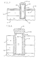
- a trench 20 extends through n-well 14 and epitaxial layer 12 to monocrystalline substrate 10. As shown in Figure 1, the trench 20 is elongated (i.e., it runs along the surface of wafer 100). A series of these trenches are formed in parallel.
- the trench 20 is filled with two layers of doped polysilicon.
- the first layer of polysilicon 22 is formed along the sidewalls of the trench.
- the second layer of polysilicon 24 fills the trench. Note that both layers of polysilicon 22, 24 extend from the trench 20 to a point above the surface of wafer 100.
- the processing method for forming this "overfill" structure will be described below.
- a first dielectric layer 26 insulates the first layer of polysilicon 22 from substrate 100.
- the second dielectric layer 26A insulates the second polysilicon layer 24 from the first polysilicon layer 22.
- a layer of silicon oxide 28 is formed over the upper surface of the trench fill. Note that the silicon oxide region 28 has lateral portions 28A that extend beyond the sides of the trench fill.
- a field effect transistor is formed on either side of the trench 20.
- Each FET includes a sidewall-defined gate electrode 34 insulated from wafer 100 by a gate insulator 34A, a diffused source electrode 36 and a diffused drain electrode 38.
- the gate electrode is part of a continuous word line that is disposed on either side of the trench 20 so that all of the FETs on one side of the trench can be accessed at the same time (see Figure 1).
- the diffusion region 38 serves as a shared drain electrode for adjacent FETs that access adjacent trench capacitors.
- the drain electrode 38 is coupled at a contact area 44 to a bit line conductor 42, which is disposed in a direction orthogonal to that of the trench 20 to couple a plurality of the drain electrodes 38 together to form a memory array (see Figure 1).
- the source diffusion 36 is coupled by a sidewall-defined bridge contact 30 to the portion of the first polysilicon layer 22 that extends above the surface of the epitaxial region 12.
- the bridge 30 is insulated from the gate electrode 34 by a sidewall-defined insulating layer 32.
- bit line 42 voltages on bit line 42 are coupled from the drain diffusion 38 to the source diffusion 36 when the gate electrode 34 is at a high voltage.
- the bridge contact 30 insures that the voltage of polysilicon layer 22 is the same as that of source diffusion 36.
- Thick polysilicon layer 24, the second dielectric layer 26A and the thin polysilicon layer 22 form a "poly-to-poly” storage capacitance.
- the thin polysilicon layer 22, the first dielectric layer 26 and the wafer 100 form a "poly-to-substrate" storage capacitance.
- the dielectric layers 26, 26A provide a dual poly-to-poly and poly-to-substrate storage capacitance whose charge/discharge is controlled by the voltage state of the thin polysilicon layer 22 coupled to the source diffusions 36 on each side of the trench.
- the charge storage capacity of one of the capacitors can be greater than that of the other. It has been found that oxide formed on polysilicon may have surface discontinuities that may promote hot carrier injection. The effect of these injected carriers may be minimized by increasing the thickness of the dielectric layer.
- the second dielectric 26A is thicker than the first dielectric 26, such that the poly-to-poly storage capacitance is enhanced.
- the poly-to-poly storage capacitance is enhanced.
- the enhanced poly-to-poly and enhanced poly-to-substrate capacitances greatly increase the composite storage capacitance at each side of the trench, such that a greater amount of charge may be stored in a smaller lithographic space.
- the ability to store more charge in less space is essential as the dynamic random access memory chips of the future reach densities of one million storage cells per chip and beyond.
- Figure 1 shows a top view of a section of an array of memory cells of the present invention.
- the word lines 34 forming the gate electrodes of the FETs run parallel to the trench 20. Note that the FETs are disposed in a spaced relationship along each side of the trench 20. The spaces between the cells are defined by thick isolation layer 28 that are disposed orthogonally with respect to trench 20 to isolate adjacent cells that access the same side of the same trench from each other.
- each memory cell takes up a chip surface area in the order of four lithographic squares, a "square” being defined as the minimum image size that can be printed using a given photolithographic exposure system.
- each cell uses one-half the width of the lithographically-defined drain diffusion 38 (that is, because the drain diffusion 38 is shared by two adjacent cells that access adjacent trenches, the lithographic space is divided between the cells), the entire width of the sidewall-defined gate electrode 34 (which, due to its self-aligned properties, may have a width that is less than the photolithographic limits), and one-half the width of the lithographically-defined trench 20; going from bottom to top within the hatched box, each memory cell uses one-half the width of a first lithographically-defined isolation region 28, the full width of the lithographically-defined bit line 42, and one-half the width of a second lithographically-defined isolation region 28. Since each side of the box is approximately (1/2+1+1/2), the total area of each cell in the order of four lithographic squares or less.
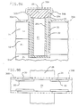
- Figure 3 shows a cross-sectional view of the isolation region between memory cells.
- Trench 20 is filled with only a single layer of polysilicon 24.
- insulating layer 26A (and possibly a residual portion of insulating layer 26, not shown) separates polysilicon 24 from the monocrystalline silicon in the isolation regions.
- An insulating layer 28 is formed uniformly over the substrate in the isolation regions.
- gate electrodes 34 are formed over the insulating layer 28 (see Figure 1).
- An epitaxial layer 12 is first grown on a substrate 10. Both the epitaxial layer 12 and the substrate 10 are doped with boron. The dopant concentrations are controlled such that the substrate 10 has a much greater concentration than does the epitaxial layer 12. The higher P concentration in substrate 10 tends to promote recombination of any majority carriers that may be injected through epitaxial layer 12. Moreover, the difference in dopant concentration produces an electric field that will tend to oppose the injection of minority carriers (i.e., electrons) from the active devices into the substrate. Such injection would materially alter the threshold voltages of the transistors, to thus seriously degrade the reliability of the various circuits formed on the chip.
- minority carriers i.e., electrons
- a layer of silicon dioxide 50 is grown on the substrate.
- the silicon dioxide is grown using conventional techniques, such as exposing the substrate to an oxidizing atmosphere (e.g., wet O2) at a temperature of approximately 800°C.
- the silicon dioxide layer should be of sufficient thickness (e.g., 30 nm) to retard crystal dislocations in the substrate that may be imparted by film stresses induced by overlaying layers.
- a layer of silicon nitride 52 is then deposited on the silicon oxide layer.
- the silicon nitride layer is formed using low pressure chemical vapor deposition (LPCVD) techniques, using NH3 and SiH2Cl2 as the deposition gasses. Typically, this nitride layer is grown to 40 nm in thickness.
- LPCVD low pressure chemical vapor deposition
- a layer of N+ type polycrystalline silicon 54 is then formed on the nitride layer 32 using conventional chemical vapor deposition techniques.
- the silicon layer is typically in the order of one micron in thickness.
- arsenic or phosphorus based gases are introduced at a sufficient concentration such that the layer 54 is N+ doped.
- One or more layers are then deposited on the upper surface of the N+ silicon layer. These layers protect the N+ silicon layer during subsequent processing. As will be described in more detail below, these layers also serve as an etch-stop when the trench fill is replanarized. For example, if chemical-mechanical polishing techniques are used, these layers should have a much slower polish rate than silicon such that the trench fill etch substantially stops when these layers are exposed. If a reactive ion etch (RIE) is used to etch back the trench fill, these layers should be substantially etch resistant in the gas ambient used to etch silicon. In the invention, layers of silicon dioxide 56 (50-75 nm) and silicon nitride 58 (100 nm) are deposited on top of the N+ silicon layer to form the etch-stop.
- RIE reactive ion etch
- a photosensitive polymer 60 is then applied on top of the upper nitride layer, and a RIE etch sequence is then used to etch through all of the overlaying layers to form trench 20 at least 5.0 ⁇ m deep into epi layer 12 and substrate 10.
- the resulting structure is shown in Figure 4.
- the polymer 60 (which may be any commercially available photoresist) is exposed and developed in the conventional manner.
- a sequence of etch ambients are introduced to anisotropically etch the stack of layers formed on substrate 10.
- the upper and lower silicon oxide layers 56 and 50, respectively, and the upper and lower silicon nitride layers 58 and 52 can be etched in a CF4 plasma.
- the N+ silicon layer 54 and the silicon substrate 10 may be etched in any plasma (e.g. a chlorine-based RIE) that produces an anisotropic profile in silicon.
- any remaining photoresist 60 may be removed using wet etch (n-methyl pyrrolidone) or dry etch (02 plasma) techniques.
- the first conformal layer 26 is made of a composite structure of silicon oxide (4 nm) - silicon nitride (4-7 nm) - silicon oxide (2 nm) that is formed by oxidizing the trench sidewalls, then depositing the silicon nitride using CVD techniques, and then oxidizing the nitride. While other dielectrics (e.g. silicon oxynitride) could be used, it has been found that the above composite structure provides the combination of low D.C. leakage, high dielectric constant, and high breakdown voltage that is needed for high density dynamic RAM applications as in the present invention.
- dielectrics e.g. silicon oxynitride
- the second conformal layer 22 is a 50 nm layer of undoped polysilicon, formed by conventional techniques.
- the third conformal layer 62 is a layer of CVD silicon oxide that is doped with boron ions. These layers are then reactive ion etched so that layers 62 and 22 are removed from the surface of silicon nitride 58 and from the trench bottom. Note that the etch is terminated after polysilicon layer 22 is completely removed from silicon nitride layer 58, such that dielectric layer 26 remains on the bottom of the trench to isolate the remaining portions of polysilicon layer 22 on each side of the trench. Due to the anisotropic nature of the RIE, all three layers remain on the sidewalls of trench 20. The upper portions of the layers are tapered due to partial attack during the RIE.
- Figures 6A-6B show a top view of the substrate at two discrete points in this process sequence.
- masking structure 64 is applied to the substrate.
- the masking structure 64 is used to expose lateral portions of the doped oxide layer 62 formed on the sidewalls of trench 20.
- the masking structure is formed of upper and lower patterned layers.
- the lower layer must be formed of a flowable material (e.g. photoresist or polyimide) that can fill portions of the trench 20.
- the upper layer After the upper layer is patterned through a photoresist, the upper layer forms a mask through which exposed portions of the lower layer are removed. Note that the compositions of the upper and lower layers must be chosen so that the upper layer is not etched while the lower layer is being patterned. Numerous layers (e.g. two photoresist layers having different etch characteristics, two polyimide layers at different levels of curing, or an upper layer of silicon oxide or nitride or silicon combined with a lower layer of polyimide or photoresist) could be used to form the upper and lower layers of the multi-layered masking structure 64. Portions of trench 20 exposed by mask 64 are then plasma etched to remove doped oxide layer 62 from the trench sidewalls.
- two photoresist layers having different etch characteristics, two polyimide layers at different levels of curing, or an upper layer of silicon oxide or nitride or silicon combined with a lower layer of polyimide or photoresist could be used to form the upper and lower layers of the multi-layered masking structure
- an anneal is carried out to drive the boron dopant ions from the remaining doped oxide 62 into the undoped polysilicon 22.
- the anneal may be carried out in an inert atmosphere such as N2.
- the anneal step may be carried out in an oxidizing atmosphere. Any oxide formed thereby is removed along with oxide layers 62 and 56 by buffered HF etching. Since the doped oxide was heavily doped, a large amount of dopant ions pass from the doped glass into the thin polysilicon layer. Then, the undoped portions of polysilicon layer 22 are selectively removed, resulting in the structure shown in Figure 6B.
- a second insulating layer 26A is applied to the structure.
- the insulating layer 26A forms a dielectric that covers the doped polysilicon layer 22 and the exposed first insulating layer 26.
- the second insulating layer 26A is formed of a composite oxide-nitride-oxide structure, as was the first insulating layer 26.
- a layer of P+ doped polysilicon 24 is applied to the structure to over-fill the trench 20.
- the doped polysilicon 24 may be formed using conventional techniques (e.g., CVD using silane as the source gas). The polysilicon 24 is then etched back so that it is planar with etch-stop layer 58.
- any one of a number of known planarization techniques can be used to planarize the polysilicon fill to etch-stop layer 58.
- chemical-mechanical polishing is preferred.
- the exposed surface of the polysilicon fill 24 is oxidized by exposure to an oxidizing atmosphere, forming a 200 nm silicon oxide cap 66. See Figure 7.
- the oxide cap 66 As a mask, the nitride layer 58 and underlaying oxide layer 56 is removed by exposure to a CF4 RIE. Then, the N+ layer 54 is removed by exposure to a wet nitric/HF - based etchant that does not appreciably attack the oxide cap 66 or the underlying nitride layer 52.
- the resulting "mandrel structure" i.e., portions of poly layers 22 and 24 and dielectric layers 26 and 26A which form a trench overfill that vertically extends above the silicon surface is shown in Figure 7.
- a conventional N-well photolithographic mask is then formed by deposition, exposure and development of a photoresist layer.
- CMOS complementary metal-oxide-semiconductor
- all of the memory cells are formed in the N-well.
- CMOS is preferred for the low power consumption it provides for the memory support circuits such as the data buffers, decoders, drivers, etc., it is to be understood that (with minor modifications) the memory cells of the invention could be formed directly in a P-type region.
- the N-well 14 is formed by phosphorus implantation at 1017 ions/cm3 into the memory cell regions, so that it extends through a substantial portion (e.g. two-thirds) of the thickness of the epitaxial layer.
- nitride is deposited on the substrate, to help define those regions in which oxide isolation is to be formed.
- the 20 nm nitride is then RIE etched to remove it from horizontal surfaces, leaving it on the mandrel sidewalls. It is necessary to stop this etch step in time to leave intact ⁇ 50% of the underlying 30 nm nitride layer 52.
- the remaining nitride 52 is anisotropically etched through a photolithographic mask to define those areas of the surface where isolation regions are to be formed.
- S-ROX semi-recessed oxidation
- the nitride layer (including the portions thereof on the sidewalls of the trench overfill) is etched by wet etching techniques (e.g. hot H3PO4). Note that nitride layer 52 is also removed during this step. Then, a brief plasma etch sequence is completed to remove the remaining nitride and oxide components of dielectric layer 26 as well as oxide layer so, such that the polysilicon layer 22 is exposed. The resulting structure is shown in Figure 8.
- wet etching techniques e.g. hot H3PO4
- a conformal layer of polysilicon 30A is then deposited on the structure, using the same techniques that were utilized to form polysilicon layer 22.
- the conformal layer is anisotropically etched in a RIE mode, such that portions 30B remain only on the sidewalls of the trench fill and isolation region 28. Because of the lateral portion 28A of the oxide isolation region 28, a small horizontal portion of the conformal layer is protected (and hence not removed) during the anisotropic etch.
- an anneal is carried out in an inert ambient at approximately 800°C so that boron diffuses from the polysilicon layer 22 into the vertical portion of the conformal layer of polysilicon, and through the horizontal portion of the polysilicon layer 22 into a portion of the n-well 14 thereunder to form a diffusion region 36 self-aligned to the conformal layer.
- the conductivity of the conformal layer may be controlled without resorting to doping the layer through conventional photolithographic techniques. Note that, similarly to the initial doping of polysilicon 22, the boron diffuses laterally so that the spacing between adjacent boron doped regions is less than the photolithographic limits (see Figure 9B).
- the polysilicon layer is exposed to an etchant (KOH in alcohol for example) that has a high undoped polysilicon-to-doped polysilicon selectivity, such that (as shown in Figure 9B) undoped portions of polysilicon region 30B that are removed, leaving doped polysilicon region 30 to form a conductive bridge that establishes contact between the polysilicon layer 22 and the P+ diffusion 36 formed thereunder by boron outdiffusion.
- an etchant KOH in alcohol for example
- the polysilicon bridge contact 30 is totally self-aligned with respect to both the polysilicon 22 and the contacted P+ diffusion 36. Again, this eliminates several costly mask-and-etch steps.
- a conformal layer of silicon oxide is applied using conventional CVD techniques. Similarly to the polysilicon layer 30A, this layer of oxide is then anisotropically etched (preferably in an 02 RIE) to form a sidewall insulator 32 (see Figure 1) that isolates the conductive bridge 30 from other conductors.
- a gate insulator 34A is formed on the exposed silicon substrate. See Figure 1.
- this gate insulator is formed by thermal oxidation of the exposed silicon.
- a thick layer of conformal polysilicon is deposited over the entire structure, and similarly to previous steps the polysilicon is anisotropically etched in a RIE mode to form sidewall-defined gate electrodes 34.
- Forming the gate electrode by sidewall techniques reduces the achievable channel length, in that the lateral length of the gate electrode is now a function of the thickness of the polysilicon as-deposited rather than being a function of the limits of the photolithographic exposure system.
- boron ions are implanted into areas of the substrate exposed by the gate electrode, and an anneal cycle is carried out to diffuse these dopant ions into the substrate to produce the drain diffusion 38.
- boron dopant ions will continue to diffuse from the portion of conductive bridge 30 overlaying the substrate, expanding the self-aligned P-type source diffusion 36 to underlap the poly silicon gate electrode.
- concentration of the sequence of 1/4+ diffusions is not critical except that it must be above about 7 ⁇ 1019/cm3 to produce the preferential etching selectivity.
- the manufacturing process is then completed by depositing a thick layer of doped glass (PSG or BPSG) 40, lithographically defining openings through the glass, and depositing a layer of metal 42 to contact the drain diffusions 38 at a juncture 44.
- PSG doped glass
- BPSG BPSG
- a sequence of sidewall-defined structures (contact bridge 30, insulating layer 32, and gate electrode 34) are all formed relative to the trench overfill, to establish the electrical and physical coupling of the filled trench 20 to the transfer gate FET.
- the resulting memorycell has a sufficient charge storage capability to be useful in a highly dense dynamic RAM chip design.
- a particularly good way of forming this stack includes the following steps.
- the exposed silicon is first oxidized by introducing an HCl/02 gas flow at 800°C for 13 minutes, and annealing the structure at 800°C for 10 minutes in an inert atmosphere.
- the resulting oxide layer is on the order of 4 nm thick.
- the wafer is exposed to a gas combination of N2 (nominal), NH3 (130 sccm), and SiH2Cl2 (10 sccm) for a sufficient time to create a 7 nm nitride layer having an index of refraction of 1.95-2.05. Then the wafer is subjected to a dry 02 (15 minutes at 1000°C) dry 02 - wet 02 - dry 02 oxidation sequence (all at 1000°C for a time sufficient to form a 2 nm thick layer of silicon oxide on the nitride.
- the second important component of the processing sequence is the ability to diffuse boron dopant from the highly doped oxide 62 to poly 22, from poly 22 to the conducting bridge 30, and from the conducting bridge 30 to the substrate surface to form a P+ source region 36 in an N-well 14. At the high minimum concentration of 7 ⁇ 1019 ions/cm3, this diffusion is reasonably forgiving, (i.e. it does not require control tighter than about ⁇ 50%).
Applications Claiming Priority (2)
| Application Number | Priority Date | Filing Date | Title |
|---|---|---|---|
| US06/919,940 US4785337A (en) | 1986-10-17 | 1986-10-17 | Dynamic ram cell having shared trench storage capacitor with sidewall-defined bridge contacts and gate electrodes |
| US919940 | 1986-10-17 |
Publications (3)
| Publication Number | Publication Date |
|---|---|
| EP0264858A2 true EP0264858A2 (de) | 1988-04-27 |
| EP0264858A3 EP0264858A3 (en) | 1989-06-28 |
| EP0264858B1 EP0264858B1 (de) | 1994-03-23 |
Family
ID=25442904
Family Applications (1)
| Application Number | Title | Priority Date | Filing Date |
|---|---|---|---|
| EP87115186A Expired - Lifetime EP0264858B1 (de) | 1986-10-17 | 1987-10-16 | Dynamische RAM-Zelle mit einem gemeinsamen Grabenspeicherkondensator, welcher durch die Seitenwände definierte Brückenkontakte und Torelektroden aufweist |
Country Status (5)
| Country | Link |
|---|---|
| US (1) | US4785337A (de) |
| EP (1) | EP0264858B1 (de) |
| JP (1) | JPS63120462A (de) |
| CA (1) | CA1289243C (de) |
| DE (1) | DE3789416T2 (de) |
Cited By (7)
| Publication number | Priority date | Publication date | Assignee | Title |
|---|---|---|---|---|
| EP0398249A2 (de) * | 1989-05-15 | 1990-11-22 | Kabushiki Kaisha Toshiba | Halbleiterspeichervorrichtung |
| EP0418491A2 (de) * | 1989-07-25 | 1991-03-27 | Texas Instruments Incorporated | DRAM-Zelle mit Grabenkondensator und vergrabenen Seitenkontakten |
| EP0428732A1 (de) * | 1989-03-23 | 1991-05-29 | Oki Electric Industry Company, Limited | Verfahren zur herstellung von halbleiteranordnungen |
| GB2238428A (en) * | 1989-11-20 | 1991-05-29 | Samsung Electronics Co Ltd | Capacitors in DRAM cells |
| EP0436073A2 (de) * | 1990-01-05 | 1991-07-10 | International Business Machines Corporation | Ein-Transistor-Speicherzelle und -matrix mit Grabenkondensator für dynamische Speichervorrichtung mit wahlfreiem Zugriff |
| EP0543158A2 (de) * | 1991-11-22 | 1993-05-26 | International Business Machines Corporation | Herstellungsverfahren von einer leitenden Verbindung in einer Halbleitervorrichtung |
| EP0591084A2 (de) * | 1992-10-02 | 1994-04-06 | International Business Machines Corporation | Struktur der Seitenflächen von Nuten |
Families Citing this family (44)
| Publication number | Priority date | Publication date | Assignee | Title |
|---|---|---|---|---|
| JPH0821685B2 (ja) * | 1988-02-26 | 1996-03-04 | 株式会社東芝 | 半導体メモリの製造方法 |
| JPH0262073A (ja) * | 1988-08-26 | 1990-03-01 | Mitsubishi Electric Corp | 半導体記憶装置 |
| JP2633650B2 (ja) * | 1988-09-30 | 1997-07-23 | 株式会社東芝 | 半導体記憶装置およびその製造方法 |
| US5001525A (en) * | 1989-03-27 | 1991-03-19 | International Business Machines Corporation | Two square memory cells having highly conductive word lines |
| JPH03276752A (ja) * | 1990-03-27 | 1991-12-06 | Matsushita Electron Corp | 半導体容量装置 |
| US5204281A (en) * | 1990-09-04 | 1993-04-20 | Motorola, Inc. | Method of making dynamic random access memory cell having a trench capacitor |
| USRE39665E1 (en) | 1992-03-13 | 2007-05-29 | Micron Technology, Inc. | Optimized container stacked capacitor DRAM cell utilizing sacrificial oxide deposition and chemical mechanical polishing |
| US5162248A (en) * | 1992-03-13 | 1992-11-10 | Micron Technology, Inc. | Optimized container stacked capacitor DRAM cell utilizing sacrificial oxide deposition and chemical mechanical polishing |
| KR950012731A (ko) * | 1993-10-25 | 1995-05-16 | 사토 후미오 | 반도체기억장치 및 그 제조방법 |
| US5529197A (en) * | 1994-12-20 | 1996-06-25 | Siemens Aktiengesellschaft | Polysilicon/polycide etch process for sub-micron gate stacks |
| US5521118A (en) * | 1994-12-22 | 1996-05-28 | International Business Machines Corporation | Sidewall strap |
| US6653733B1 (en) * | 1996-02-23 | 2003-11-25 | Micron Technology, Inc. | Conductors in semiconductor devices |
| US6197644B1 (en) * | 1998-11-06 | 2001-03-06 | Advanced Micro Devices, Inc. | High density mosfet fabrication method with integrated device scaling |
| US6531071B1 (en) * | 2000-01-04 | 2003-03-11 | Micron Technology, Inc. | Passivation for cleaning a material |
| US6573550B2 (en) * | 2000-01-28 | 2003-06-03 | General Electronics Applications, Inc. | Semiconductor with high-voltage components and low-voltage components on a shared die |
| JP2002076308A (ja) * | 2000-08-31 | 2002-03-15 | Fujitsu Ltd | 半導体装置およびその製造方法 |
| US6498062B2 (en) * | 2001-04-27 | 2002-12-24 | Micron Technology, Inc. | DRAM access transistor |
| US7231624B2 (en) * | 2002-11-19 | 2007-06-12 | Cadence Design Systems, Inc. | Method, system, and article of manufacture for implementing metal-fill with power or ground connection |
| US7287324B2 (en) * | 2002-11-19 | 2007-10-30 | Cadence Design Systems, Inc. | Method, system, and article of manufacture for implementing metal-fill on an integrated circuit |
| US7328419B2 (en) * | 2002-11-19 | 2008-02-05 | Cadence Design Systems, Inc. | Place and route tool that incorporates a metal-fill mechanism |
| US6734524B1 (en) * | 2002-12-31 | 2004-05-11 | Motorola, Inc. | Electronic component and method of manufacturing same |
| JP2004228342A (ja) * | 2003-01-23 | 2004-08-12 | Denso Corp | 半導体装置およびその製造方法 |
| KR20040096377A (ko) * | 2003-05-09 | 2004-11-16 | 삼성전자주식회사 | 산화막 및 산질화막 형성 방법 |
| US8334451B2 (en) * | 2003-10-03 | 2012-12-18 | Ixys Corporation | Discrete and integrated photo voltaic solar cells |
| TWI231960B (en) * | 2004-05-31 | 2005-05-01 | Mosel Vitelic Inc | Method of forming films in the trench |
| US7518179B2 (en) | 2004-10-08 | 2009-04-14 | Freescale Semiconductor, Inc. | Virtual ground memory array and method therefor |
| JP4667821B2 (ja) * | 2004-10-13 | 2011-04-13 | シャープ株式会社 | 半導体装置 |
| US7314798B2 (en) * | 2005-07-25 | 2008-01-01 | Freescale Semiconductor, Inc. | Method of fabricating a nonvolatile storage array with continuous control gate employing hot carrier injection programming |
| US7285819B2 (en) * | 2005-07-25 | 2007-10-23 | Freescale Semiconductor, Inc. | Nonvolatile storage array with continuous control gate employing hot carrier injection programming |
| US20070020840A1 (en) * | 2005-07-25 | 2007-01-25 | Freescale Semiconductor, Inc. | Programmable structure including nanocrystal storage elements in a trench |
| US7112490B1 (en) * | 2005-07-25 | 2006-09-26 | Freescale Semiconductor, Inc. | Hot carrier injection programmable structure including discontinuous storage elements and spacer control gates in a trench |
| US7394686B2 (en) * | 2005-07-25 | 2008-07-01 | Freescale Semiconductor, Inc. | Programmable structure including discontinuous storage elements and spacer control gates in a trench |
| US7619270B2 (en) * | 2005-07-25 | 2009-11-17 | Freescale Semiconductor, Inc. | Electronic device including discontinuous storage elements |
| US7619275B2 (en) * | 2005-07-25 | 2009-11-17 | Freescale Semiconductor, Inc. | Process for forming an electronic device including discontinuous storage elements |
| US7582929B2 (en) * | 2005-07-25 | 2009-09-01 | Freescale Semiconductor, Inc | Electronic device including discontinuous storage elements |
| US7642594B2 (en) * | 2005-07-25 | 2010-01-05 | Freescale Semiconductor, Inc | Electronic device including gate lines, bit lines, or a combination thereof |
| US7262997B2 (en) * | 2005-07-25 | 2007-08-28 | Freescale Semiconductor, Inc. | Process for operating an electronic device including a memory array and conductive lines |
| US7694258B1 (en) * | 2005-08-01 | 2010-04-06 | Cadence Design Systems, Inc. | Method and apparatus for inserting metal fill in an integrated circuit (“IC”) layout |
| US7592224B2 (en) | 2006-03-30 | 2009-09-22 | Freescale Semiconductor, Inc | Method of fabricating a storage device including decontinuous storage elements within and between trenches |
| US7572699B2 (en) * | 2007-01-24 | 2009-08-11 | Freescale Semiconductor, Inc | Process of forming an electronic device including fins and discontinuous storage elements |
| US7651916B2 (en) | 2007-01-24 | 2010-01-26 | Freescale Semiconductor, Inc | Electronic device including trenches and discontinuous storage elements and processes of forming and using the same |
| US7838922B2 (en) * | 2007-01-24 | 2010-11-23 | Freescale Semiconductor, Inc. | Electronic device including trenches and discontinuous storage elements |
| DE102007009383A1 (de) * | 2007-02-20 | 2008-08-21 | Fraunhofer-Gesellschaft zur Förderung der angewandten Forschung e.V. | Halbleiteranordnung und Verfahren zu deren Herstellung |
| KR101218904B1 (ko) * | 2010-11-29 | 2013-01-21 | 심재훈 | 메모리 소자 및 이의 제조 방법 |
Citations (4)
| Publication number | Priority date | Publication date | Assignee | Title |
|---|---|---|---|---|
| EP0083816A1 (de) * | 1981-12-31 | 1983-07-20 | Koninklijke Philips Electronics N.V. | Halbleiteranordnung mit einem Verbindungsmuster |
| EP0164829A1 (de) * | 1984-04-19 | 1985-12-18 | Nippon Telegraph And Telephone Corporation | Halbleiterspeicherbauelement und Verfahren zur Herstellung |
| JPS6187359A (ja) * | 1984-10-05 | 1986-05-02 | Nec Corp | 半導体メモリセル |
| EP0198590A2 (de) * | 1985-04-16 | 1986-10-22 | Kabushiki Kaisha Toshiba | Halbleiterspeichervorrichtung |
Family Cites Families (14)
| Publication number | Priority date | Publication date | Assignee | Title |
|---|---|---|---|---|
| US32090A (en) * | 1861-04-16 | Clothes-wbiitgee | ||
| US3387286A (en) * | 1967-07-14 | 1968-06-04 | Ibm | Field-effect transistor memory |
| CA1144646A (en) * | 1978-09-20 | 1983-04-12 | Junji Sakurai | Dynamic ram having buried capacitor and planar gate |
| US4256514A (en) * | 1978-11-03 | 1981-03-17 | International Business Machines Corporation | Method for forming a narrow dimensioned region on a body |
| US4369564A (en) * | 1979-10-29 | 1983-01-25 | American Microsystems, Inc. | VMOS Memory cell and method for making same |
| US4378627A (en) * | 1980-07-08 | 1983-04-05 | International Business Machines Corporation | Self-aligned metal process for field effect transistor integrated circuits using polycrystalline silicon gate electrodes |
| US4322883A (en) * | 1980-07-08 | 1982-04-06 | International Business Machines Corporation | Self-aligned metal process for integrated injection logic integrated circuits |
| US4419809A (en) * | 1981-12-30 | 1983-12-13 | International Business Machines Corporation | Fabrication process of sub-micrometer channel length MOSFETs |
| JPS59141262A (ja) * | 1983-02-02 | 1984-08-13 | Nec Corp | 半導体メモリセル |
| JPS6068647A (ja) * | 1983-09-26 | 1985-04-19 | Fujitsu Ltd | 半導体記憶装置 |
| JPH0665225B2 (ja) * | 1984-01-13 | 1994-08-22 | 株式会社東芝 | 半導体記憶装置の製造方法 |
| US4688063A (en) * | 1984-06-29 | 1987-08-18 | International Business Machines Corporation | Dynamic ram cell with MOS trench capacitor in CMOS |
| JPS6187358A (ja) * | 1984-10-05 | 1986-05-02 | Nec Corp | 半導体記憶装置およびその製造方法 |
| JPS6188555A (ja) * | 1984-10-08 | 1986-05-06 | Nec Corp | 半導体メモリセル |
-
1986
- 1986-10-17 US US06/919,940 patent/US4785337A/en not_active Expired - Fee Related
-
1987
- 1987-08-06 JP JP62195438A patent/JPS63120462A/ja active Granted
- 1987-10-16 DE DE3789416T patent/DE3789416T2/de not_active Expired - Fee Related
- 1987-10-16 EP EP87115186A patent/EP0264858B1/de not_active Expired - Lifetime
- 1987-10-19 CA CA000549648A patent/CA1289243C/en not_active Expired - Fee Related
Patent Citations (4)
| Publication number | Priority date | Publication date | Assignee | Title |
|---|---|---|---|---|
| EP0083816A1 (de) * | 1981-12-31 | 1983-07-20 | Koninklijke Philips Electronics N.V. | Halbleiteranordnung mit einem Verbindungsmuster |
| EP0164829A1 (de) * | 1984-04-19 | 1985-12-18 | Nippon Telegraph And Telephone Corporation | Halbleiterspeicherbauelement und Verfahren zur Herstellung |
| JPS6187359A (ja) * | 1984-10-05 | 1986-05-02 | Nec Corp | 半導体メモリセル |
| EP0198590A2 (de) * | 1985-04-16 | 1986-10-22 | Kabushiki Kaisha Toshiba | Halbleiterspeichervorrichtung |
Non-Patent Citations (1)
| Title |
|---|
| PATENT ABSTRACTS OF JAPAN, vol. 10, no. 259 (E-434)[2315], 4th September 1986; & JP-A-61 087 359 (NEC CORP.) 02-05-1986 * |
Cited By (16)
| Publication number | Priority date | Publication date | Assignee | Title |
|---|---|---|---|---|
| EP0428732A4 (en) * | 1989-03-23 | 1991-07-03 | Oki Electric Industry Company, Limited | Method of producing semiconductor devices |
| US5120677A (en) * | 1989-03-23 | 1992-06-09 | Oki Electric Industry Co., Ltd. | Method for making a semiconductor device by doping with arsenic, of at least 25 wt. % into a polysilicon layer |
| EP0428732A1 (de) * | 1989-03-23 | 1991-05-29 | Oki Electric Industry Company, Limited | Verfahren zur herstellung von halbleiteranordnungen |
| EP0398249A3 (de) * | 1989-05-15 | 1991-06-26 | Kabushiki Kaisha Toshiba | Halbleiterspeichervorrichtung |
| EP0398249A2 (de) * | 1989-05-15 | 1990-11-22 | Kabushiki Kaisha Toshiba | Halbleiterspeichervorrichtung |
| EP0418491A3 (en) * | 1989-07-25 | 1991-09-25 | Texas Instruments Incorporated | Dram cell with trench capacitor and buried lateral contact |
| EP0418491A2 (de) * | 1989-07-25 | 1991-03-27 | Texas Instruments Incorporated | DRAM-Zelle mit Grabenkondensator und vergrabenen Seitenkontakten |
| GB2238428A (en) * | 1989-11-20 | 1991-05-29 | Samsung Electronics Co Ltd | Capacitors in DRAM cells |
| GB2238428B (en) * | 1989-11-20 | 1993-07-14 | Samsung Electronics Co Ltd | Semiconductor device and manufacturing method thereof |
| EP0436073A2 (de) * | 1990-01-05 | 1991-07-10 | International Business Machines Corporation | Ein-Transistor-Speicherzelle und -matrix mit Grabenkondensator für dynamische Speichervorrichtung mit wahlfreiem Zugriff |
| EP0436073A3 (en) * | 1990-01-05 | 1993-05-26 | International Business Machines Corporation | Trench-capacitor-one-transistor storage cell and array for dynamic random access memories |
| EP0543158A2 (de) * | 1991-11-22 | 1993-05-26 | International Business Machines Corporation | Herstellungsverfahren von einer leitenden Verbindung in einer Halbleitervorrichtung |
| EP0543158A3 (en) * | 1991-11-22 | 1993-12-29 | Ibm | Method of conducting strap formation in a semiconductor device |
| EP0591084A2 (de) * | 1992-10-02 | 1994-04-06 | International Business Machines Corporation | Struktur der Seitenflächen von Nuten |
| EP0591084A3 (de) * | 1992-10-02 | 1994-12-07 | Ibm | Struktur der Seitenflächen von Nuten. |
| US5521114A (en) * | 1992-10-02 | 1996-05-28 | International Business Machines Corporation | Trench sidewall structure |
Also Published As
| Publication number | Publication date |
|---|---|
| EP0264858A3 (en) | 1989-06-28 |
| DE3789416D1 (de) | 1994-04-28 |
| DE3789416T2 (de) | 1994-10-27 |
| CA1289243C (en) | 1991-09-17 |
| JPS63120462A (ja) | 1988-05-24 |
| EP0264858B1 (de) | 1994-03-23 |
| US4785337A (en) | 1988-11-15 |
| JPH0586072B2 (de) | 1993-12-09 |
Similar Documents
| Publication | Publication Date | Title |
|---|---|---|
| EP0264858B1 (de) | Dynamische RAM-Zelle mit einem gemeinsamen Grabenspeicherkondensator, welcher durch die Seitenwände definierte Brückenkontakte und Torelektroden aufweist | |
| US4833094A (en) | Method of making a dynamic ram cell having shared trench storage capacitor with sidewall-defined bridge contacts and gate electrodes | |
| US4353086A (en) | Silicon integrated circuits | |
| US5406515A (en) | Method for fabricating low leakage substrate plate trench DRAM cells and devices formed thereby | |
| US6204112B1 (en) | Process for forming a high density semiconductor device | |
| US5770484A (en) | Method of making silicon on insulator buried plate trench capacitor | |
| EP0474258A1 (de) | Verfahren zur Herstellung eines dynamischen Halbleiterspeichers | |
| EP0398249B1 (de) | Halbleiterspeichervorrichtung | |
| US6849529B2 (en) | Deep-trench capacitor with hemispherical grain silicon surface and method for making the same | |
| US6459610B1 (en) | Semiconductor-on-insulator transistor, memory circuitry employing semiconductor-on-insulator transistors, method of forming a semiconductor-on-insulator transistor, and method of forming memory circuitry employing semiconductor-on-insulator transistors | |
| US5156993A (en) | Fabricating a memory cell with an improved capacitor | |
| US6566202B2 (en) | Integrated circuit having at least two vertical MOS transistors and method for manufacturing same | |
| US20040235240A1 (en) | Method of fabricating memory device with vertical transistors and trench capacitors | |
| KR100570114B1 (ko) | 자기 정렬 매립형 극판 | |
| KR0171072B1 (ko) | 반도체 메모리 셀 제조방법 및 구조 | |
| US6677197B2 (en) | High aspect ratio PBL SiN barrier formation | |
| US6929998B2 (en) | Method for forming bottle-shaped trench | |
| US4958206A (en) | Diffused bit line trench capacitor dram cell | |
| US4897702A (en) | Semiconductor memory device and manufacturing method for the same | |
| US6355517B1 (en) | Method for fabricating semiconductor memory with a groove | |
| USRE32090E (en) | Silicon integrated circuits | |
| US5300800A (en) | Low leakage substrate plate DRAM cell | |
| US6916703B2 (en) | Method for forming uniform bottom electrode in trench of trench capacitor | |
| US6204528B1 (en) | Dynamic random access memory structure | |
| JPH08111512A (ja) | 半導体記憶装置及びその製造方法 |
Legal Events
| Date | Code | Title | Description |
|---|---|---|---|
| PUAI | Public reference made under article 153(3) epc to a published international application that has entered the european phase |
Free format text: ORIGINAL CODE: 0009012 |
|
| AK | Designated contracting states |
Kind code of ref document: A2 Designated state(s): DE FR GB IT |
|
| 17P | Request for examination filed |
Effective date: 19880823 |
|
| PUAL | Search report despatched |
Free format text: ORIGINAL CODE: 0009013 |
|
| AK | Designated contracting states |
Kind code of ref document: A3 Designated state(s): DE FR GB IT |
|
| 17Q | First examination report despatched |
Effective date: 19910517 |
|
| GRAA | (expected) grant |
Free format text: ORIGINAL CODE: 0009210 |
|
| AK | Designated contracting states |
Kind code of ref document: B1 Designated state(s): DE FR GB IT |
|
| REF | Corresponds to: |
Ref document number: 3789416 Country of ref document: DE Date of ref document: 19940428 |
|
| ITF | It: translation for a ep patent filed |
Owner name: IBM - DR. ING. FABRIZIO LETTIERI |
|
| ET | Fr: translation filed | ||
| PLBE | No opposition filed within time limit |
Free format text: ORIGINAL CODE: 0009261 |
|
| STAA | Information on the status of an ep patent application or granted ep patent |
Free format text: STATUS: NO OPPOSITION FILED WITHIN TIME LIMIT |
|
| 26N | No opposition filed | ||
| PGFP | Annual fee paid to national office [announced via postgrant information from national office to epo] |
Ref country code: GB Payment date: 19950926 Year of fee payment: 9 |
|
| PGFP | Annual fee paid to national office [announced via postgrant information from national office to epo] |
Ref country code: DE Payment date: 19951030 Year of fee payment: 9 |
|
| PGFP | Annual fee paid to national office [announced via postgrant information from national office to epo] |
Ref country code: FR Payment date: 19961007 Year of fee payment: 10 |
|
| PG25 | Lapsed in a contracting state [announced via postgrant information from national office to epo] |
Ref country code: GB Effective date: 19961016 |
|
| GBPC | Gb: european patent ceased through non-payment of renewal fee |
Effective date: 19961016 |
|
| PG25 | Lapsed in a contracting state [announced via postgrant information from national office to epo] |
Ref country code: DE Effective date: 19970701 |
|
| PG25 | Lapsed in a contracting state [announced via postgrant information from national office to epo] |
Ref country code: FR Free format text: THE PATENT HAS BEEN ANNULLED BY A DECISION OF A NATIONAL AUTHORITY Effective date: 19971031 |
|
| REG | Reference to a national code |
Ref country code: FR Ref legal event code: ST |
|
| PG25 | Lapsed in a contracting state [announced via postgrant information from national office to epo] |
Ref country code: IT Free format text: LAPSE BECAUSE OF NON-PAYMENT OF DUE FEES;WARNING: LAPSES OF ITALIAN PATENTS WITH EFFECTIVE DATE BEFORE 2007 MAY HAVE OCCURRED AT ANY TIME BEFORE 2007. THE CORRECT EFFECTIVE DATE MAY BE DIFFERENT FROM THE ONE RECORDED. Effective date: 20051016 |