EP0543158A2 - Herstellungsverfahren von einer leitenden Verbindung in einer Halbleitervorrichtung - Google Patents
Herstellungsverfahren von einer leitenden Verbindung in einer Halbleitervorrichtung Download PDFInfo
- Publication number
- EP0543158A2 EP0543158A2 EP92117856A EP92117856A EP0543158A2 EP 0543158 A2 EP0543158 A2 EP 0543158A2 EP 92117856 A EP92117856 A EP 92117856A EP 92117856 A EP92117856 A EP 92117856A EP 0543158 A2 EP0543158 A2 EP 0543158A2
- Authority
- EP
- European Patent Office
- Prior art keywords
- polysilicon
- silicon
- layer
- etching
- diffusion
- Prior art date
- Legal status (The legal status is an assumption and is not a legal conclusion. Google has not performed a legal analysis and makes no representation as to the accuracy of the status listed.)
- Withdrawn
Links
Images


Classifications
-
- H—ELECTRICITY
- H01—ELECTRIC ELEMENTS
- H01L—SEMICONDUCTOR DEVICES NOT COVERED BY CLASS H10
- H01L21/00—Processes or apparatus adapted for the manufacture or treatment of semiconductor or solid state devices or of parts thereof
- H01L21/02—Manufacture or treatment of semiconductor devices or of parts thereof
- H01L21/04—Manufacture or treatment of semiconductor devices or of parts thereof the devices having at least one potential-jump barrier or surface barrier, e.g. PN junction, depletion layer or carrier concentration layer
- H01L21/18—Manufacture or treatment of semiconductor devices or of parts thereof the devices having at least one potential-jump barrier or surface barrier, e.g. PN junction, depletion layer or carrier concentration layer the devices having semiconductor bodies comprising elements of Group IV of the Periodic System or AIIIBV compounds with or without impurities, e.g. doping materials
- H01L21/30—Treatment of semiconductor bodies using processes or apparatus not provided for in groups H01L21/20 - H01L21/26
- H01L21/31—Treatment of semiconductor bodies using processes or apparatus not provided for in groups H01L21/20 - H01L21/26 to form insulating layers thereon, e.g. for masking or by using photolithographic techniques; After treatment of these layers; Selection of materials for these layers
- H01L21/3205—Deposition of non-insulating-, e.g. conductive- or resistive-, layers on insulating layers; After-treatment of these layers
- H01L21/321—After treatment
- H01L21/3213—Physical or chemical etching of the layers, e.g. to produce a patterned layer from a pre-deposited extensive layer
- H01L21/32133—Physical or chemical etching of the layers, e.g. to produce a patterned layer from a pre-deposited extensive layer by chemical means only
- H01L21/32134—Physical or chemical etching of the layers, e.g. to produce a patterned layer from a pre-deposited extensive layer by chemical means only by liquid etching only
-
- H—ELECTRICITY
- H01—ELECTRIC ELEMENTS
- H01L—SEMICONDUCTOR DEVICES NOT COVERED BY CLASS H10
- H01L21/00—Processes or apparatus adapted for the manufacture or treatment of semiconductor or solid state devices or of parts thereof
- H01L21/70—Manufacture or treatment of devices consisting of a plurality of solid state components formed in or on a common substrate or of parts thereof; Manufacture of integrated circuit devices or of parts thereof
- H01L21/71—Manufacture of specific parts of devices defined in group H01L21/70
- H01L21/768—Applying interconnections to be used for carrying current between separate components within a device comprising conductors and dielectrics
- H01L21/76838—Applying interconnections to be used for carrying current between separate components within a device comprising conductors and dielectrics characterised by the formation and the after-treatment of the conductors
- H01L21/76895—Local interconnects; Local pads, as exemplified by patent document EP0896365
Definitions
- This invention relates to strap formation in a semiconductor device, and more particularly to electrical connection of a first silicon region to a second silicon region when the two regions are separated by a dielectric. Straps (electrical connections) and methods for their formation are provided.
- conductive structures typically have large numbers of conductive structures which need to be interconnected.
- Such conductive structures include, for example, silicon regions separated by a dielectric region.
- the conductive structures are interconnected by forming a "bridge contact" or "strap" between the structures.
- Refractory metals and refractory metal silicides have often been used for interconnecting conductive structures. These materials possess low resistivity characteristics normally associated with metals such as aluminum and copper, without providing the manufacturing challenges inherent in these materials (heat sensitivity in the case of aluminum, patterning difficulties in the case of copper).
- silicide electrodes are formed on silicon diffusion regions by depositing the refractory metal layer on the substrate, heating the metal to form silicide regions over the exposed silicon regions, and treating the substrate in a wet etchant to remove the unreacted refractory metal.
- This silicide forming method poses problems in that the method may consume up to several microns of the underlaying silicon in forming the silicide. This consumption has the effect of greatly reducing the effective dopant concentrations at the silicide/diffusion interface, which can have negative effects on the characteristics of the semiconductor device.
- U.S. Patent No. 4,502,894 (issued March 5, 1985) discloses a process for producing polysilicon resistors, by employing boron out- diffusion. After forming oxide regions, boron or other dopant is implanted into the oxide. A layer of polysilicon is then deposited and patterned, and the structure is treated to cause boron to out-diffuse into the polysilicon.
- Japanese Patent No. 62-122124 discloses a process for out-diffusion of boron into an overlying polysilicon layer. After a silicon dioxide film is grown onto a silicon substrate a boron phosphorus silicate glass (BPSG) film is deposited. A contact hole is then formed in the BPSG and the oxide layers, followed by deposition of a polysilicon layer. The structure is then heated to effect boron out-diffusion from the BPSG layer into the polysilicon layer.
- BPSG boron phosphorus silicate glass
- U.S. Patent No. 4,654,121 discloses a process for forming stacked CMOS devices. After forming the lower device, an undoped oxide layer and then a doped oxide layer are formed. A planarizing step is then carried out to expose the gate electrode and to form doped oxide regions to the sides of the gate. An upper gate oxide is grown and a polysilicon layer defined over the oxide. The source and drain regions for the upper device are then formed by boron out-diffusion from the lower doped oxide regions.
- U.S. Patent No. 4,782,036 (issued November 1, 1988) discloses a process for doping the sidewalls and base of a trench. After the trench formation in a silicon substrate, a borosilicate glass layer is deposited by decomposition of TEOS and trimethylborate. Then, the structure is treated to cause boron to diffuse into the sidewalls and base, followed by removal of the glass layer.
- the strap is electrically conductive and connects conductive structures within the semiconductor device.
- the present invention is directed to a process for forming a contact between a polysilicon-filled trench and an adjacent diffusion region, separated by a dielectric.
- the process involves performing a shallow boron implant, and then depositing a diffusion barrier layer (generally, silicon nitride or aluminum oxide).
- a diffusion barrier layer generally, silicon nitride or aluminum oxide.
- the barrier layer is patterned to form openings where the contacts are to be formed.
- a layer of intrinsic polysilicon is deposited using low pressure chemical vapor deposition (LPCVD) over the substrate, i.e. over the barrier layer and in the contact openings.
- LPCVD low pressure chemical vapor deposition
- an anneal is carried out to diffuse boron into the polysilicon.
- the "lightly doped" portions of the polysilicon are removed with a wet etchant so as to form the desired polysilicon contacts.
- the remaining polysilicon is then oxidized, to protect the polysilicon from silicide formation during subsequent processing.
- doping refers to the addition of impurities to a semiconductor material. Doping allows the manufacture of n-type and p-type semiconductors with varying degrees of conductivity. In general, the greater the extent of doping, the higher the conductivity.
- n-type material refers to a semiconductor material that has been doped with a donor-type impurity and, consequently, conducts a current via electrons.
- a p-type material refers to a semiconductor material that has been doped with an acceptor-type impurity and, consequently, conducts a current via hole migration.
- Etching refers to chemically eating away a metal to form a desired pattern as an etched circuit, an etched circuit referring to a circuit produced by etching the conductive coating of a substrate to provide the required pattern of conductors and terminals to which discrete components are connected.
- Selectively etching refers to the use of etching, for example, in the manufacture of circuits, to remove selected portions of one material from another in a semiconductor structure.
- a capacitor refers to a passive electronic circuit component consisting of, in basic form, two conductive electrodes or plates separated by a dielectric (or insulator).
- a trench capacitor refers to a capacitor formed in a trench in the surface of a semiconductor substrate.
- a stacked capacitor refers to a capacitor formed by stacking the capacitor above the semiconductor substrate.
- RIE reactive ion etching
- Passivation refers to the process of growing a thin oxide film on the surface of a planar semiconductor device to protect the exposed junction(s) from contamination and shorts, with sidewall passivation referring to this process in relation to sidewalls.
- CVD refers to chemical vapor deposition, with chemical deposition being the coating of a surface with a substance resulting from chemical reaction on the surface.
- LPCVD refers to low pressure chemical vapor deposition.
- Ion implantation refers to the implantation of ions, for example, for doping a semiconductor substrate.
- Silicon as used in this application, includes polysilicon (polycrystalline silicon), amorphous silicon (non-crystalline silicon), and monocrystalline silicon. Such silicon may be n- or p-doped, or undoped.
- the broad concept of the subject invention is directed to a method for electrically connecting a first silicon area to a second silicon area when the first and second silicon areas are separated by a dielectric.
- the first and second silicon areas each have an exposed surface, as well as the dielectric. The method comprises the steps of:
- the first silicon area comprises a polysilicon-filled trench and the second silicon area comprises a diffusion region, separated by silicon dioxide.
- the silicon areas are doped with boron using ion implantation.
- the dopant can comprise BF2, in which case an annealing step is required to outgas the fluorine.
- the continuous diffusion barrier layer in one embodiment comprises silicon nitride, but could also comprise aluminum oxide or silicon dioxide.
- the diffusion barrier layer is preferably deposited using chemical vapor deposition.
- a mask is then applied over the diffusion barrier layer to define a pattern which includes the area where the electrical connection (or strap) will be formed.
- the unmasked portions of the diffusion barrier layer are then etched, for example, using reactive ion etching.
- a continuous layer of polysilicon is then deposited over the remaining diffusion barrier layer and also over the underlying surfaces exposed by the removal of portions of the diffusion barrier layer.
- this deposition comprises chemical vapor deposition.
- a critical step in the disclosed method is the diffusion of the dopant from the first and second silicon areas into the continuous layer of polysilicon.
- the dopant will not diffuse through the remaining diffusion barrier layer, therefore the dopant will only diffuse into the continuous layer of polysilicon corresponding to the position where the diffusion barrier layer had previously been etched away.
- the diffusion comprises annealing at about 900° C for about 5 minutes, which results in diffusion of the boron to a distance of about 0.2 microns into the layer of polysilicon.
- the resulting structure is then wet etched, such as with potassium hydroxide/isopropyl alcohol (KOH/IPA) or other suitable alcohol, or ethylenediamine, pyrocatechol and water (EPW), so as to remove the portions of the continuous layer of polysilicon into which no dopant diffused.
- KOH/IPA potassium hydroxide/isopropyl alcohol
- EPW ethylenediamine, pyrocatechol and water
- Any remaining diffusion barrier layer is then etched away, preferably using reactive ion etching.
- the remaining portion of the continuous layer of polysilicon forms the electrical connection (strap) between the first silicon and second silicon areas (or polysilicon-filled trench and diffusion region), which are separated by a dielectric.
- the invention further provides an electrically conductive strap for connecting a first silicon area and a second silicon area formed by the method discussed above.
- the first silicon area in the strap formation comprises a polysilicon- filled trench and the second silicon area comprises a diffusion region.
- the polysilicon-filled trench and the diffusion region are separated by a dielectric.
- the invention provides a "Boron out-diffused surface strap” or “BOSS” and a method of forming the strap.
- BOSS Backbone out-diffused surface strap
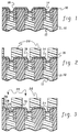
- the BOSS process as depicted in Figures 1-10 is as follows.
- an additional boron ion implantation 16 is performed which raises the near surface concentration well above solid solubility.
- 2E15 BF2 at 10 keV was utilized.
- nitride 18 is deposited using low pressure chemical vapor deposition (LPCVD), preferably silicon nitride to a thickness of 250 ⁇ (see FIG. 1).
- LPCVD low pressure chemical vapor deposition
- a layer of resist 20 is then applied to serve as a surface strap mask for reactive ion etching of the nitride layer.
- the nitride 18 is etched 22 at area 24 which is where the strap is to go. This area 24 includes the top surface 26 of the p+ region, the top surface 28 of the dielectric, and the top surface 30 of the trench.
- the resist layer is removed and a layer of intrinsic polysilicon 32 is then applied over the entire structure using LPCVD.
- the deposited polysilicon is 1200 ⁇ thick.
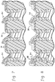
- FIG. 5 shows the step of boron out-diffusion (represented by arrows to indicate the diffusion of the boron), or annealing, wherein boron diffuses into the deposited polysilicon to define the strap. In one embodiment, annealing was at 900° C for 5 minutes.
- FIG. 6 shows the step of wet etching, for example using potassium hydroxide/isopropyl alcohol (KOH/IPA) or other suitable alcohol; or ethylenediamene, pyrocatechol and water (EPW), to remove "lightly doped” polysilicon (the etching represented by arrows).
- the lightly doped polysilicon is that polysilicon which has not been further doped during the boron out-diffusion step, i.e. that polysilicon deposited over the nitride layer.
- the remaining polysilicon corresponds to the area 24 in FIG. 3 and represents the strap 34 as shown in FIG. 7.
- RIE is then utilized to remove the remaining nitride layer 18 as also shown in FIG. 7.
- the strap 34 remains interconnecting the diffusion region 10 and the polysilicon-filled trench 12, separated by a dielectric 14 (see FIG. 8).
- a layer of titanium silicide 36 can then be applied over remaining silicon and/or polysilicon regions. Specifically, a layer of titanium is deposited over the entire structure and heated to cause reaction between the titanium and any underlying silicon or polysilicon. The resulting titanium silicide allows lower resistance, and the unreacted titanium is removed using any suitable means known to those skilled in the art.
- the purpose of the additional ion implantation at the P+ junction formation is to provide a reservoir of boron which will last throughout the strap diffusion step. Since the standard semiconductor junction already raises the concentration above solid solubility, this additional ion implantation causes no change in the junction depth. For an ion implantation of 1E15 or greater there is no increase in strap length. That is, for doses greater than this, the boron reservoir has not been depleted at the end of diffusion.
- a fluorine out-gas anneal is required.
- Preferred conditions for the fluorine out-gas anneal are 700° C for 20 minutes, but this can be replaced by a hold in the low pressure nitride deposition after insertion but before putting on the reactant vapors.
- the preferred anneal cycle of 900° C for 5 minutes was chosen to give 0.2 microns of "out-diffused" strap formation.
- diffusing at higher temperatures may result in a more robust strap.
- boron solid solubility increases with temperature, the poly strap will be more highly doped.
- KOH/IPA etch selectivity is a strong function of doping level.
- the strap thickness is 600-800 ⁇ after a 100% over-etch in KOH/IPA.
- the strap is expected to be close to 1200 ⁇ after etch for diffusion at higher temperatures (1000° C).
- the strap extends only this distance up the side of the gate stack. This is contrasted with the previously known straps which extend up the entire length of the Gate stack. This should decrease the incidence of Gate to node shorts. It will also decrease word line Gate capacitance.
- TTO refers to "trench top open” and refers to removing oxide over the trenches after the whole surface is planarized and the gate conductors are formed. It is important that oxide over the trenches be etched out before masking for the nitride etch, or after the nitride is patterned. In the case of masked TTO, where the oxide over the trench is etched after the nitride is patterned, the boron skin implant is done after the patterned resist for nitride etching is removed (see below).
- this invention further provides a short oxidation which can be easily integrated into the BOSS process to oxidize the strap polysilicon selectively. Oxidation of the strap polysilicon provides each individual strap with its own insulation, thus isolating the straps from the TiSi2 formation process. Since the straps are individually insulated, shorting to adjacent cells is avoided unless out-diffusion length exceeds half of the linear distance between the edges of two adjacent strap holes.
- FIG. 9 This optional oxidation step is depicted in FIG. 9 and FIG. 10.
- a layer of oxide 38 is formed on the strap 34'.
- the strap oxidation is performed before the removal of the barrier Si3N4 layer so that oxidation occurs only on the polysilicon straps.
- FIG. 10 shows the strap 34' with the oxide layer 38 after the remaining nitride layer has been removed, and the titanium silicide layer 36' over the remaining silicon and/or polysilicon regions.
- the strap oxidation step is incorporated into the original BOSS process described above. Added heat cycle time due to the oxidation is found to have negligible effect on junction depth.
- This oxidation step is based on the principle that the amount of out-diffusion required to strap the trench capacitor to the diffusion region is equal to half of the linear distance from the edge of the diffusion region to the edge of the recessed trench.
- the maximum allowable out-diffusion is governed by the linear distance measured from the edge of the strap hole to the adjacent diffusion region or trench. While the thin nitride layer provides insulation underneath the polysilicon straps, subsequent TiSi2 formation atop of the strap connecting the diffusion region and the trench would short the strap, at random, to adjacent diffusion region or trench. In addition, depletion of boron due to boron segregation during and after the TiSi2 formation process can result in highly resistive straps with undesirable non-ohmic behavior. Insulation of the straps from TiSi2 alleviates this problem.
Applications Claiming Priority (2)
| Application Number | Priority Date | Filing Date | Title |
|---|---|---|---|
| US07/797,506 US5185294A (en) | 1991-11-22 | 1991-11-22 | Boron out-diffused surface strap process |
| US797506 | 1991-11-22 |
Publications (2)
| Publication Number | Publication Date |
|---|---|
| EP0543158A2 true EP0543158A2 (de) | 1993-05-26 |
| EP0543158A3 EP0543158A3 (en) | 1993-12-29 |
Family
ID=25171021
Family Applications (1)
| Application Number | Title | Priority Date | Filing Date |
|---|---|---|---|
| EP19920117856 Withdrawn EP0543158A3 (en) | 1991-11-22 | 1992-10-19 | Method of conducting strap formation in a semiconductor device |
Country Status (3)
| Country | Link |
|---|---|
| US (1) | US5185294A (de) |
| EP (1) | EP0543158A3 (de) |
| JP (1) | JP2501734B2 (de) |
Cited By (7)
| Publication number | Priority date | Publication date | Assignee | Title |
|---|---|---|---|---|
| EP0651433A1 (de) * | 1993-11-02 | 1995-05-03 | Siemens Aktiengesellschaft | Verfahren zur Herstellung eines Kontaktlochs zu einem dotierten Bereich |
| US5731218A (en) * | 1993-11-02 | 1998-03-24 | Siemens Aktiengesellschaft | Method for producing a contact hole to a doped region |
| WO1999033113A1 (de) * | 1997-12-18 | 1999-07-01 | Siemens Aktiengesellschaft | Halbleiterspeicher, herstellverfahren für den halbleiterspeicher und implantationsmaske |
| DE19906292C1 (de) * | 1999-02-15 | 2000-03-30 | Siemens Ag | Elektrische Teststruktur auf einem Halbleitersubstrat und Testverfahren |
| DE19906291A1 (de) * | 1999-02-15 | 2000-08-24 | Siemens Ag | Halbleiterstruktur mit einer Leitbahn |
| US6815358B2 (en) | 2001-09-06 | 2004-11-09 | Seagate Technology Llc | Electron beam lithography method for plating sub-100 nm trenches |
| EP1525613A1 (de) * | 2002-07-30 | 2005-04-27 | Infineon Technologies AG | VERWENDUNG VON MASKEN AUS METALLOXIDEN ZUR BEARBEITUNG VON OBERFLäCHEN BEI DER HERSTELLUNG VON MIKROCHIPS |
Families Citing this family (24)
| Publication number | Priority date | Publication date | Assignee | Title |
|---|---|---|---|---|
| JP2914000B2 (ja) * | 1992-04-28 | 1999-06-28 | 日本電気株式会社 | 半導体装置の製造方法 |
| US5431777A (en) * | 1992-09-17 | 1995-07-11 | International Business Machines Corporation | Methods and compositions for the selective etching of silicon |
| US5521118A (en) * | 1994-12-22 | 1996-05-28 | International Business Machines Corporation | Sidewall strap |
| US5543348A (en) * | 1995-03-29 | 1996-08-06 | Kabushiki Kaisha Toshiba | Controlled recrystallization of buried strap in a semiconductor memory device |
| KR100247724B1 (ko) * | 1995-09-01 | 2000-03-15 | 포만 제프리 엘 | 실리사이드화된 접촉 영역을 갖는 확산 저항 구조 및 그의 제조 방법 |
| US5905279A (en) * | 1996-04-09 | 1999-05-18 | Kabushiki Kaisha Toshiba | Low resistant trench fill for a semiconductor device |
| US5923971A (en) * | 1996-10-22 | 1999-07-13 | International Business Machines Corporation | Reliable low resistance strap for trench storage DRAM cell using selective epitaxy |
| DE19713961C2 (de) * | 1997-04-04 | 1999-05-06 | Siemens Ag | Verfahren zur Erzeugung einer leitenden Verbindung zwischen zumindest zwei Gebieten eines ersten Leitfähigkeitstyps |
| JP3031294B2 (ja) * | 1997-06-06 | 2000-04-10 | 日本電気株式会社 | 半導体装置の製造方法 |
| US6074909A (en) * | 1998-07-31 | 2000-06-13 | Siemens Aktiengesellschaft | Apparatus and method for forming controlled deep trench top isolation layers |
| US6100172A (en) * | 1998-10-29 | 2000-08-08 | International Business Machines Corporation | Method for forming a horizontal surface spacer and devices formed thereby |
| US6096598A (en) * | 1998-10-29 | 2000-08-01 | International Business Machines Corporation | Method for forming pillar memory cells and device formed thereby |
| US6150256A (en) * | 1998-10-30 | 2000-11-21 | International Business Machines Corporation | Method for forming self-aligned features |
| US6194268B1 (en) | 1998-10-30 | 2001-02-27 | International Business Machines Corporation | Printing sublithographic images using a shadow mandrel and off-axis exposure |
| US6190971B1 (en) | 1999-05-13 | 2001-02-20 | International Business Machines Corporation | Formation of 5F2 cell with partially vertical transistor and gate conductor aligned buried strap with raised shallow trench isolation region |
| US6339228B1 (en) * | 1999-10-27 | 2002-01-15 | International Business Machines Corporation | DRAM cell buried strap leakage measurement structure and method |
| TW451447B (en) * | 1999-12-31 | 2001-08-21 | Samsung Electronics Co Ltd | Contact structures of wirings and methods for manufacturing the same, and thin film transistor array panels including the same and methods for manufacturing the same |
| US6706634B1 (en) * | 2000-09-19 | 2004-03-16 | Infineon Technologies Ag | Control of separation between transfer gate and storage node in vertical DRAM |
| US6833321B2 (en) * | 2001-11-30 | 2004-12-21 | Intel Corporation | Method of making a semiconductor device that has copper damascene interconnects with enhanced electromigration reliability |
| JP2006093635A (ja) * | 2004-09-27 | 2006-04-06 | Toshiba Corp | 半導体装置およびその製造方法 |
| US7285472B2 (en) * | 2005-01-27 | 2007-10-23 | International Business Machines Corporation | Low tolerance polysilicon resistor for low temperature silicide processing |
| US20080251934A1 (en) * | 2007-04-13 | 2008-10-16 | Jack Allan Mandelman | Semiconductor Device Structures and Methods of Fabricating Semiconductor Device Structures for Use in SRAM Devices |
| US20080251878A1 (en) * | 2007-04-13 | 2008-10-16 | International Business Machines Corporation | Structure incorporating semiconductor device structures for use in sram devices |
| US9853055B2 (en) | 2016-03-30 | 2017-12-26 | Globalfoundries Inc. | Method to improve crystalline regrowth |
Citations (4)
| Publication number | Priority date | Publication date | Assignee | Title |
|---|---|---|---|---|
| EP0200364A1 (de) * | 1985-03-29 | 1986-11-05 | Advanced Micro Devices, Inc. | Verfahren zur Herstellung von Elektroden und Verbindungen aus Metallsilicid |
| WO1986007491A1 (en) * | 1985-06-12 | 1986-12-18 | Ncr Corporation | Process for forming contacts and interconnects for integrated circuits |
| EP0264858A2 (de) * | 1986-10-17 | 1988-04-27 | International Business Machines Corporation | Dynamische RAM-Zelle mit einem gemeinsamen Grabenspeicherkondensator, welcher durch die Seitenwände definierte Brückenkontakte und Torelektroden aufweist |
| US4830972A (en) * | 1987-02-06 | 1989-05-16 | Kabushiki Kaisha Toshiba | Method of manufacturing bipolar transistor |
Family Cites Families (10)
| Publication number | Priority date | Publication date | Assignee | Title |
|---|---|---|---|---|
| US4502894A (en) * | 1983-08-12 | 1985-03-05 | Fairchild Camera & Instrument Corporation | Method of fabricating polycrystalline silicon resistors in integrated circuit structures using outdiffusion |
| US4939104A (en) * | 1984-10-31 | 1990-07-03 | Texas Instruments, Incorporated | Method for forming a buried lateral contact |
| US4745081A (en) * | 1985-10-31 | 1988-05-17 | International Business Machines Corporation | Method of trench filling |
| JPS62122124A (ja) * | 1985-11-21 | 1987-06-03 | Mitsubishi Electric Corp | 半導体装置の製造方法 |
| US4654121A (en) * | 1986-02-27 | 1987-03-31 | Ncr Corporation | Fabrication process for aligned and stacked CMOS devices |
| US4746219A (en) * | 1986-03-07 | 1988-05-24 | Texas Instruments Incorporated | Local interconnect |
| US4782036A (en) * | 1986-08-29 | 1988-11-01 | Siemens Aktiengesellschaft | Process for producing a predetermined doping in side walls and bases of trenches etched into semiconductor substrates |
| US4983544A (en) * | 1986-10-20 | 1991-01-08 | International Business Machines Corporation | Silicide bridge contact process |
| US4745087A (en) * | 1987-01-13 | 1988-05-17 | Advanced Micro Devices, Inc. | Method of making fully self-aligned bipolar transistor involving a polysilicon collector contact formed in a slot with an oxide sidewall |
| US4873205A (en) * | 1987-12-21 | 1989-10-10 | International Business Machines Corporation | Method for providing silicide bridge contact between silicon regions separated by a thin dielectric |
-
1991
- 1991-11-22 US US07/797,506 patent/US5185294A/en not_active Expired - Fee Related
-
1992
- 1992-10-14 JP JP4302964A patent/JP2501734B2/ja not_active Expired - Lifetime
- 1992-10-19 EP EP19920117856 patent/EP0543158A3/en not_active Withdrawn
Patent Citations (4)
| Publication number | Priority date | Publication date | Assignee | Title |
|---|---|---|---|---|
| EP0200364A1 (de) * | 1985-03-29 | 1986-11-05 | Advanced Micro Devices, Inc. | Verfahren zur Herstellung von Elektroden und Verbindungen aus Metallsilicid |
| WO1986007491A1 (en) * | 1985-06-12 | 1986-12-18 | Ncr Corporation | Process for forming contacts and interconnects for integrated circuits |
| EP0264858A2 (de) * | 1986-10-17 | 1988-04-27 | International Business Machines Corporation | Dynamische RAM-Zelle mit einem gemeinsamen Grabenspeicherkondensator, welcher durch die Seitenwände definierte Brückenkontakte und Torelektroden aufweist |
| US4830972A (en) * | 1987-02-06 | 1989-05-16 | Kabushiki Kaisha Toshiba | Method of manufacturing bipolar transistor |
Non-Patent Citations (2)
| Title |
|---|
| IBM TECHNICAL DISCLOSURE BULLETIN. vol. 29, no. 8 , January 1987 , NEW YORK US page 3423 'DIFFUSION DEFINED BRIDGE CONTACT' * |
| INTERNATIONAL ELECTRON DEVICES MEETING DECEMBER 6-9 1987 WASHINGTON pages 32 - 35 Y.MISAWA ET AL. 'A SELF-ALIGNING POLYSILICON ELECTRODE TECHNOLOGY (SPEL) FOR FUTURE LSIS' * |
Cited By (10)
| Publication number | Priority date | Publication date | Assignee | Title |
|---|---|---|---|---|
| EP0651433A1 (de) * | 1993-11-02 | 1995-05-03 | Siemens Aktiengesellschaft | Verfahren zur Herstellung eines Kontaktlochs zu einem dotierten Bereich |
| DE4337355A1 (de) * | 1993-11-02 | 1995-05-04 | Siemens Ag | Verfahren zur Herstellung eines Kontaktlochs zu einem dotierten Bereich |
| US5731218A (en) * | 1993-11-02 | 1998-03-24 | Siemens Aktiengesellschaft | Method for producing a contact hole to a doped region |
| WO1999033113A1 (de) * | 1997-12-18 | 1999-07-01 | Siemens Aktiengesellschaft | Halbleiterspeicher, herstellverfahren für den halbleiterspeicher und implantationsmaske |
| DE19906292C1 (de) * | 1999-02-15 | 2000-03-30 | Siemens Ag | Elektrische Teststruktur auf einem Halbleitersubstrat und Testverfahren |
| DE19906291A1 (de) * | 1999-02-15 | 2000-08-24 | Siemens Ag | Halbleiterstruktur mit einer Leitbahn |
| US6310361B1 (en) | 1999-02-15 | 2001-10-30 | Infineon Technologies Ag | Electrical test structure on a semiconductor substrate and test method |
| US6724055B2 (en) | 1999-02-15 | 2004-04-20 | Infineon Technologies Ag | Semiconductor structure having an interconnect and method of producing the semiconductor structure |
| US6815358B2 (en) | 2001-09-06 | 2004-11-09 | Seagate Technology Llc | Electron beam lithography method for plating sub-100 nm trenches |
| EP1525613A1 (de) * | 2002-07-30 | 2005-04-27 | Infineon Technologies AG | VERWENDUNG VON MASKEN AUS METALLOXIDEN ZUR BEARBEITUNG VON OBERFLäCHEN BEI DER HERSTELLUNG VON MIKROCHIPS |
Also Published As
| Publication number | Publication date |
|---|---|
| US5185294A (en) | 1993-02-09 |
| EP0543158A3 (en) | 1993-12-29 |
| JP2501734B2 (ja) | 1996-05-29 |
| JPH07193023A (ja) | 1995-07-28 |
Similar Documents
| Publication | Publication Date | Title |
|---|---|---|
| US5185294A (en) | Boron out-diffused surface strap process | |
| US5545581A (en) | Plug strap process utilizing selective nitride and oxide etches | |
| US5405806A (en) | Method for forming a metal silicide interconnect in an integrated circuit | |
| US4312680A (en) | Method of manufacturing submicron channel transistors | |
| US6987041B2 (en) | Semiconductor device having both memory and logic circuit and its manufacture | |
| JP2889137B2 (ja) | 低漏洩基板プレート・トレンチdramセルを製作する方法及びそれにより形成されるデバイス | |
| US5173450A (en) | Titanium silicide local interconnect process | |
| EP0188291B1 (de) | Bipolare Halbleiteranordnung und Verfahren zu ihrer Herstellung | |
| EP0289163B1 (de) | Verfahren zur Herstellung einer Silicid-Halbleiterelement mit Polysilizium-Bereiche | |
| CA1241458A (en) | Side-etching method of making bipolar transistor | |
| EP0033495B1 (de) | Verfahren zur Herstellung eines bipolaren Transistors mit hoher Geschwindigkeit | |
| EP0463458B1 (de) | Verfahren und Struktur zur Verbindung von verschiedenen Zonen aus Polysilizium für integrierte Schaltkreise | |
| EP0051500B1 (de) | Halbleiterbauelement | |
| JPH0152907B2 (de) | ||
| Okamoto et al. | Simultaneous formation of TiN and TiSi2 by lamp annealing in NH3 ambient and its application to diffusion barriers | |
| US5550085A (en) | Method for making a buried contact | |
| US6184129B1 (en) | Low resistivity poly-silicon gate produced by selective metal growth | |
| US5612239A (en) | Use of oxide spacers formed by liquid phase deposition | |
| US5888875A (en) | Diffusion resistor structure with silicided contact areas, and methods of fabrication thereof | |
| JPH0691210B2 (ja) | Dramセル用高性能トレンチコンデンサ | |
| US5670417A (en) | Method for fabricating self-aligned semiconductor component | |
| US5946595A (en) | Method of forming a local interconnect between electronic devices on a semiconductor substrate | |
| EP0231740A2 (de) | Selbstjustierendes bipolares Bauelement aus Polysilizium und Verfahren zu seiner Herstellung | |
| EP0264309B1 (de) | Selbstausgerichteter Basis-Nebenschluss für einen Transistor | |
| KR100403355B1 (ko) | 반도체소자의제조방법 |
Legal Events
| Date | Code | Title | Description |
|---|---|---|---|
| PUAI | Public reference made under article 153(3) epc to a published international application that has entered the european phase |
Free format text: ORIGINAL CODE: 0009012 |
|
| AK | Designated contracting states |
Kind code of ref document: A2 Designated state(s): DE FR GB |
|
| PUAL | Search report despatched |
Free format text: ORIGINAL CODE: 0009013 |
|
| 17P | Request for examination filed |
Effective date: 19930918 |
|
| AK | Designated contracting states |
Kind code of ref document: A3 Designated state(s): DE FR GB |
|
| 17Q | First examination report despatched |
Effective date: 19950724 |
|
| STAA | Information on the status of an ep patent application or granted ep patent |
Free format text: STATUS: THE APPLICATION IS DEEMED TO BE WITHDRAWN |
|
| 18D | Application deemed to be withdrawn |
Effective date: 19960206 |