EP0260992B1 - Dispositif de commande de gradation pour des appareils d'impression du type à transfert thermique d'encre - Google Patents
Dispositif de commande de gradation pour des appareils d'impression du type à transfert thermique d'encre Download PDFInfo
- Publication number
- EP0260992B1 EP0260992B1 EP87308301A EP87308301A EP0260992B1 EP 0260992 B1 EP0260992 B1 EP 0260992B1 EP 87308301 A EP87308301 A EP 87308301A EP 87308301 A EP87308301 A EP 87308301A EP 0260992 B1 EP0260992 B1 EP 0260992B1
- Authority
- EP
- European Patent Office
- Prior art keywords
- datum
- voltage drop
- heating
- voltage
- data
- Prior art date
- Legal status (The legal status is an assumption and is not a legal conclusion. Google has not performed a legal analysis and makes no representation as to the accuracy of the status listed.)
- Expired - Lifetime
Links
Images


Classifications
-
- H—ELECTRICITY
- H04—ELECTRIC COMMUNICATION TECHNIQUE
- H04N—PICTORIAL COMMUNICATION, e.g. TELEVISION
- H04N1/00—Scanning, transmission or reproduction of documents or the like, e.g. facsimile transmission; Details thereof
- H04N1/40—Picture signal circuits
- H04N1/40025—Circuits exciting or modulating particular heads for reproducing continuous tone value scales
- H04N1/4005—Circuits exciting or modulating particular heads for reproducing continuous tone value scales with regulating circuits, e.g. dependent upon ambient temperature or feedback control
-
- H—ELECTRICITY
- H04—ELECTRIC COMMUNICATION TECHNIQUE
- H04N—PICTORIAL COMMUNICATION, e.g. TELEVISION
- H04N1/00—Scanning, transmission or reproduction of documents or the like, e.g. facsimile transmission; Details thereof
- H04N1/40—Picture signal circuits
- H04N1/40025—Circuits exciting or modulating particular heads for reproducing continuous tone value scales
- H04N1/40031—Circuits exciting or modulating particular heads for reproducing continuous tone value scales for a plurality of reproducing elements simultaneously
Definitions
- the present invention generally relates to gradation (or density) control devices for thermal ink-transfer type printing apparatuses (hereinafter simply referred to as thermal printers), and more particularly to a gradation control device which controls the size of printing dots by controlling an applying time of a constant current which is applied to heating elements of a thermal printing head in order to control the gradation level or printing density in a thermal printer.
- thermal printers thermal ink-transfer type printing apparatuses
- thermal printers are being developed as one of the more promising type and are used in copying machines, facsimile machines and the like.
- the thermal printer employs an ink film which is a polyester film having a thickness of 5 to 6 microns coated with a kind of ink which melts due to heat on one surface thereof.
- the ink film is placed onto a recording sheet with the ink side making contact with the recording sheet, and a thermal printing head makes contact with a rear side of the ink film.
- the thermal printing head comprises a plurality of heating elements arranged in a row, and a current is applied to each of these heating elements which are to be heated.
- the density which determines the gradation level of the printed characters, diagrams, pictures and the like, is determined by the area of each dot formed on the recording sheet. And, this area of the melted ink dot is determined according to the current applied to each of the heating elements. Generally, the heat value becomes larger as the magnitude of the current applied to the heating element becomes larger. As a result, the area of the melted ink dot becomes larger to increase the printing density, and the gradation level reaches near a saturated density. Accordingly, the magnitudes of the currents applied to the heating elements are conventionally controlled in order to control the gradation level of the printing. However, the currents applied to the heating elements are generally large currents in the order of 5 to 20 Amperes.
- EP-A-0 130 417 discloses a thermal printer which monitors the current through at least one of the thermal elements of the print head, the printer terminates the printing of a line when none of the thermal elements conducts a current and proceeds to the next line, thereby reducing printing time.
- the power source voltage may be corrected by remote sensing, for example. But the correction of the power source voltage by the remote sensing is insufficient in that the response speed is too slow in the case where the heating elements of the thermal printing head are driven by pulse currents.
- a gradation control device for a thermal ink-transfer type printing apparatus, said printing apparatus comprising a power source and a thermal printing head coupled to said power source through a transmission path and provided with n heating elements arranged in line, said n heating elements heating an ink film coated with a kind of ink which melts due to heat and transferring the melted ink onto a recording sheet which makes contact with the ink sheet to print images line by line, said gradation control device comprising memory means for storing at least n digital data of natural binary code which represent gradation levels with which the printing is to be carried out; converting means including means for repeatedly reading out the n digital data from said memory means in response to a clock pulse signal having a constant repetition frequency m times in a time period in which one line is printed and means for generating a reference printing density datum a value of which is changed every time the n digital data are read out once, said converting means producing control data in a form of a serial n-bit data signal having
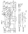
- FIG.1 shows an embodiment of the gradation control device according to the present invention.
- a thermal printing head 16 comprises a ceramic substrate and n heating elements (heating resistors) R1 through Rn provided on the substrate, where n is an integer greater than or equal to two.
- the printing head 16 is positioned on an ink film 11 shown in FIG.2, and the n heating elements R1 through Rn are arranged in-line in a width direction of the ink film 11.
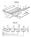
- the gradation control device may be applied to a thermal printer having a known construction shown in FIG.2.
- the ink film 11, acting as a transfer sheet comprises a polyester film 12 and an ink 13 of a kind which melts due to heat coated over one surface of the polyester film 12 to a predetermined thickness.
- a recording sheet 14 makes contact with the side of the ink film 11 coated with the ink 13, and is fed along a direction A by a roller 15 together with the ink film 11.
- the printing head 16 is provided opposing the roller 15, and makes contact with the rear side of the ink film 11, that is, the side of the ink film 11 not coated with the ink 13.
- the ink film 11 passes by the printing head 16, the ink film 11 is guided by a roller 17, separated from the recording sheet 14 and then taken up on a take-up spool (not shown) as a used ink film 11a.
- a transferred ink 13a remains on a printed surface 14a of the printed recording sheet 14.
- the area of the transferred ink 13a is shown as a large area in FIG.2 for convenience' sake, however, the transferred ink 13a actually is a collection of small dots.
- One dot is formed by one heating element, and the size of one dot is determined by the magnitude of the current applied to a corresponding one of the heating elements R1 through Rn or an applying time during which the current is applied to the corresponding heating element.
- the density of the printed figures and the like, that is, the gradation level, is determined by the size of each of the dots.
- the gradation control device may be applied to such a thermal printer of the type described above.
- an analog video signal from a video signal generator 18 is converted into a digital signal in an analog-to-digital (A/D) converter 19, and the digital signal is stored in a data storing device 20.
- an address counter 21 is supplied with a reference clock pulse signal from a terminal 22 and a start pulse signal from a terminal 23, and supplies an address to the data storing device 20.
- a reference printing density datum (that is, a datum of a reference gradation level, and hereinafter referred to as a second datum) successively changes from "0" which indicates a minimum printing density to "m-1" which indicates a maximum printing density, where m denotes the number of output second data of a data counter 25.
- a density data comparing circuit 24 compares the value of the second datum and the values of n first data intended for the n heating elements R1 through Rn, for each of the m printing densities.
- An n-bit datum obtained as a result of the comparison with one second datum is passed through a shift register 26 and is latched in a latch circuit 27.
- data (control data) obtained by the comparison of each of the m second data and the n first data corresponding to one printing line are successively latched in the latch circuit 27 a total of m times.
- the data storing device 20 supplies to the comparing circuit 24 one first datum (a first datum in the data obtained from the A/D converter 19) corresponding to a first address from the address counter 21. Initially, a count in the data counter 25 is set to "0" because the data counter 25 is reset by the start pulse signal from the terminal 23. The reference printing density datum (second datum) which is successively incremented according to the count is supplied to the comparing circuit 24 from the data counter 25.
- the comparing circuit 24 compares the first datum and the second datum "0" which indicates the minimum printing density, and supplies a control datum "1" when the first datum is greater than the second datum "0" and supplies a control datum "0" when the first datum is smaller than or equal to the second datum "0".
- the address counter 21 successively supplies the second, third, ..., and n-th addresses to the data storing device 20, and the data storing device 20 successively supplies to the comparing circuit 24 the first data corresponding to the second through n-th addresses.
- the first data corresponding to the first through n-th addresses respectively are the picture element data which are to be printed by the heating elements R1 through Rn.
- the comparing circuit 24 compares the second datum "0" and the first data corresponding to the second through n-th addresses, and successively supplies a control datum "0" or "1" to the shift register 26 depending on the compared results.
- the n-bit control datum from the comparing circuit 24 corresponding to the first through n-th addresses are entered into the n-stage shift register 26 by being successively shifted therein in synchronism with the reference clock pulse signal which is obtained from the terminal 22 via an AND circuit 31.
- the address counter 21 When the address counter 21 finishes counting n clock pulses and accordingly finishes outputting the first through n-th addresses, the address counter 21 supplies a data transfer pulse to the data counter 25 and the latch circuit 27. Furthermore, this data transfer pulse is also supplied to a correcting circuit 28 via a terminal 29.
- the correcting circuit 28 receives the reference clock pulse signal from the terminal 22 through a terminal 32.
- the data counter 25 supplies a heating time limiting pulse to the correcting circuit 28 via a terminal 30 responsive to the data transfer pulse.
- the data counter 21 increments the value "0" of the second datum to a value "1" which indicates the next smallest printing density to the printing density indicated by the initial value "0".
- the n-bit control datum which is entered into the shift register 26 is latched in parallel by the latch circuit 27 responsive to the data transfer pulse.
- the n-bit control datum latched by the latch circuit 27 is supplied in parallel to one of two input terminals of gate (AND) circuits G1 through Gn.
- the address counter 21 resets itself by loading data "00...0" in response to a load pulse signal generated therein responsive to a carry signal when the count in the address counter 21 exceeds the value corresponding to the n-th address.
- the address counter 21 again successively outputs the first through n-th addresses so that the data storing device 20 outputs n first data and these n first data are compared with the second datum "1" in the comparing circuit 24.
- the data counter 25, the shift register 26, the latch circuit 27, the AND circuit 31 and the like operate similarly as in the case where the second datum is "0" as described before.
- latched control datum is supplied to the gate circuits G1 through Gn.
- a corrected heating pulse from a terminal 40 of the correcting circuit 28 is applied to the other of the two input terminals of each of the gate circuits G1 through Gn.
- Output signals of the gate circuits G1 through Gn are applied to bases of corresponding NPN-type transistors T1 through Tn and controls the switching thereof.
- a current is applied to those heating elements which are coupled to collectors of the transistors which are turned ON, and the heating elements applied with the current are heated.
- a voltage drop detecting circuit 42 detects a voltage drop between a power source (not shown) and the printing head 16 and supplies a detected voltage drop datum to a terminal 43 of the correcting circuit 28. Hence, a corrected heating pulse dependent on the detected voltage drop is outputted from the terminal 40 of the correcting circuit 28.
- the comparison in the comparing circuit 24 is carried out for the first through n-th addresses with respect to all of the remaining printing densities indicated by values "2" through "m-1" in the data counter 25.
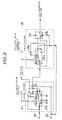
- FIG.3 shows an embodiment of the address counter 21 and the data counter 25.
- the address counter 21 comprises a counter 21a, a 2-input NAND circuit 21b and an inverter 21c.
- the data counter 25 comprises a counter 25a, an inverter 25b and a flip-flop 25c.
- the reference clock pulse signal from the terminal 22 is supplied to a clock terminal CK of the counter 21a and one input terminal of the NAND circuit 21b.
- the start pulse signal from the terminal 23 is supplied to clear terminals CLR of the counters 21a and 25a and the flip-flop 25c.
- Outputs from terminals Q0 through Q9 of the counter 21a are supplied to the data storing device 20, and an output (carry signal) from a terminal Q10 is supplied to the other input terminal of the NAND circuit 21b.
- An output of the NAND circuit 21b is supplied to a load terminal LD of the counter 21a, the inverter 21c and the AND circuit 31.
- the counter 21a loads the data "00...0" responsive to a low-level load pulse signal applied to the load terminal LD thereof.
- An output of the inverter 21c is supplied to clock terminals CK of the counter 25a and the flip-flop 25c.
- Outputs from terminals Q0 through Q5 of the counter 25a are supplied to the comparing circuit 24 and the correcting circuit 28.
- An output (carry signal) from a terminal Q6 of the counter 25a is passed through the inverter 25b and is supplied to a terminal P of the counter 25a and a data terminal D of the flip-flop 25c.
- the counter 25a holds the count when a low-level signal is supplied to the terminal P thereof and keeps this count regardless of the signal applied to the clock terminal CK of the counter 25a.
- a fixed voltage (+5 V) is applied to a preset terminal P of the flip-flop 25c, and a Q-output of the flip-flop 25c is supplied to the correcting circuit 28 as the heating time limiting pulse.
- the present embodiment is characterized in that corrected heating pulse is outputted from the correcting circuit 28 depending on the output voltage drop datum of the voltage drop detecting circuit 42 shown in FIG.1.
- the voltage drop detecting circuit 42 comprises a differential amplifier 53, an integrating circuit 54, a sample and hold (S/H) circuit 56, and an analog-to-digital (A/D) converter 58.
- a reference voltage V P and a head terminal voltage V T are applied to respective terminals 51 and 52 and are supplied to the differential amplifier 53.
- the reference voltage V P is a constant voltage and is obtained from a fixed voltage source (not shown) or by holding the power source voltage for the printing head 16 during a non-printing interval. As will be described later, the voltage drop in a transmission path between the power source and the printing head 16 can be detected by simply supplying the reference voltage V P to the terminal 51 from the power source terminal for the printing head 16.
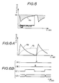
- the head terminal voltage V T varies depending on the printing data as shown in FIG.5. Accordingly, a voltage drop occurs between the reference voltage V P and the head terminal voltage V T as indicated by hatchings in FIG.5 when the current is applied to the printing head.
- the current applying time corresponds to the pulse width of the heating time limiting pulse.
- the differential amplifier 53 amplifies a voltage difference between the reference voltage V P and the head terminal voltage V T , and supplies to the integrating circuit 54 a drop voltage V D shown in FIG.6A corresponding to the voltage drop between the power source and the printing head 16.
- the integrating circuit 54 is supplied with a reset signal from a terminal 55, and this reset signal shown in FIG.6B(A) has a period amounting to the time it takes to print one line with one density (one gradation level). For example, the period of this reset signal is in the range of 15 ⁇ sec to 100 ⁇ sec. Accordingly, the integrating circuit 54 integrates the drop voltage V D for every one period of the reset signal, and produces a voltage V I indicated by phantom lines in FIG.6A. This voltage V I corresponds to the accumulated voltage drop within the current applying time, that is, the pulse width of the heating time limiting pulse.
- the voltage V I from the integrating circuit 54 is supplied to the S/H circuit 56.
- a sampling pulse signal shown in FIG.6B(B) having a period amounting to the time it takes to print one line with one density is applied to a terminal 57 and is supplied to the S/H circuit 56.
- This sampling pulse signal has such a timing that the sampling is carried out in the S/H circuit 56 when the voltage change stabilizes, that is, when the voltage V I becomes approximately constant.
- the S/H circuit 56 samples the incoming voltage V I responsive to the sampling pulse signal and holds the sampled voltage until the next sampling point, that is, for the time it takes to print one line with one density.
- the output sampled voltage of the S/H circuit 56 is supplied to the A/D converter 58.
- a clock signal shown in FIG.6B(C) is applied to a terminal 59 and is supplied to the A/D converter 58, and the A/D converter 58 converts the sampled voltage into a digital voltage drop datum shown in FIG.6B(D) responsive to the clock signal.
- FIG.7 shows a second embodiment of the voltage drop detecting circuit 42.
- the voltage drop detecting circuit 42 shown in FIG.7 comprises the differential amplifier 53, a circuit 60, and an A/D converter 62.
- the circuit 60 may either be a peak detecting circuit or a sample and hold (S/H) circuit.
- the differential amplifier 53 generates a drop voltage V D shown in FIG.8A from the reference voltage V P and the head terminal voltage V T .
- the S/H circuit 60 detects the peak voltage of the drop voltage V D based on a sampling pulse signal shown in FIG.8B(A) which is obtained from a terminal 61, and supplies to the A/D converter 62 the sampled voltage indicated by phantom lines in FIG.8A.
- the sampling pulse signal has a period amounting to the time it takes to print one line with one density.
- the peak detecting circuit 60 has no need of the pulse signal from the terminal 61 and detects the peak voltage of the drop voltage V D , and the peak voltage indicated by the phantom lines in FIG.8A is supplied to the A/D converter 62.
- the circuit 60 is reset by a reset signal shown in FIG.8B(B) which is obtained from a terminal 64.
- the A/D converter 62 converts the sampled voltage or the peak voltage from the circuit 60 into a digital voltage drop datum responsive to a clock signal shown in FIG.8B(C) which is obtained from a terminal 63. As a result, the digital voltage drop datum shown in FIG.8B(D) is supplied to the correcting circuit 28.
- the circuit construction of the second embodiment of the voltage drop detecting circuit 42 shown in FIG.7 is simple compared to that of the first embodiment shown in FIG.4, because no integrating circuit is required in the second embodiment.
- the sampled or peak value of the drop voltage V D successively changes with time depending on the external conditions, parasitic capacitance of the wires and the like.
- the first embodiment of the voltage drop detecting circuit 42 is a more desirable embodiment in that the voltage drop datum is obtained by integrating the drop voltage V D , and the stability of the first embodiment is high compared to that of the second embodiment.
- the correcting circuit 28 comprises a counter 71, a read only memory (ROM) 72, a comparator 73 and a 2-input AND circuit 74.
- the reference printing density datum (second datum) c shown in FIG.10(C) from the data counter 25 shown in FIG.1 is supplied to the ROM 72 through the terminal 33 and the output voltage drop datum of the voltage drop detecting circuit 42 shown in FIG.1 is supplied to the ROM 72 through the terminal 43, respectively as read-out address data.
- a correcting datum f shown in FIG.12(A) is read out from the ROM 72 based on the read-out address data.
- the ROM 72 pre-stores a set of correcting data amounting to the maximum number m of gradation levels, at addresses designated by each of the voltage drop data. For example, when the gradation is described in 6 bits and the voltage drop datum is described in 4 bits, the ROM 72 pre-stores 16 sets of correcting data, where each set of correcting data is made up of 64 correcting data. As will be described later, the correcting data determine the pulse width of the corrected heating pulse.
- the correcting data corresponding to an intermediate gradation level is set to a value smaller than those of the correcting data corresponding to the high and low (dark and light) gradation levels in each set of correcting data.
- the correcting data corresponding to the voltage drop data indicative of larger voltage drops have larger values so as to satisfactorily correct the voltage drop in the power source voltage supplied to the printing head 16.
- the correcting data are described in a number of bits approximately the same as the number of bits used to describe the gradation levels.
- the counter 71 is supplied with a clock pulse signal a shown in FIG.10(A) which is obtained by dividing the reference clock pulse signal from the terminal 22 shown in FIG.1 through the terminal 32 and the data transfer pulse b shown in FIG.10(B) which is obtained from the address counter 21 shown in FIG.1 through the terminal 29.
- the counter 71 generates a comparison datum d shown in FIG.10(D) which is successively incremented starting from "0", for example, every time the transfer pulse b is received.
- the comparison datum d is reset to "0" when the next transfer pulse b is received.
- This comparison datum d is supplied to the comparator 73 which is also supplied with the correcting datum f from the ROM 72, and the comparator 73 compares the two data d and f.
- the comparator 73 compares the values of the correcting datum f and the comparison datum d for every period of the data transfer pulse b shown in FIGS.10(B) and 11(B), and outputs a pulse signal e shown in FIGS.10(E) and 11(C).
- the pulse signal e has a high level when the value of the comparison datum d is smaller than the value of the correcting datum f, and has a low level when the value of the comparison datum d is greater than or equal to the value of the correcting datum f. Accordingly, the pulse width of the pulse signal e is proportional to the value of the correcting datum f read out from the ROM 72.
- the AND circuit 74 is supplied with the pulse signal e from the comparator 73 and the output heating time limiting pulse of the data counter 25 obtained through the terminal 30. But since the heating time limiting pulse has a high level essentially for the entire duration of the printing of the dot, the pulse signal e is passed through the AND circuit 74 and is supplied to the gate circuits G1 through Gn through the terminal 40 as the corrected heating pulse.
- predetermined heating elements out of the heating elements R1 through Rn are applied with the current depending on the printing data for the applying time which changes depending on the printing density of the picture element data constituting the printing data.
- the data counter 25 counts the maximum number m of gradation levels, the printing of one line on the recording sheet 14 is completed.
- the start pulse signal g shown in FIG.11(A) from the terminal 23 clears the data counter 25, and the data counter 25 again starts to count from "0" to "m-1".
- FIGS.13(A) and 13(B) are time charts for explaining the correction of the current applying time according to the voltage drop datum.
- a percentage of the number of heating elements applied with the current with respect to the total number n of the heating elements R1 through Rn will hereunder be defined as a percentage of conducting heads for convenience' sake.
- FIG.13(A) shows the correcting datum f readout from the ROM 72
- FIG.13(B) shows the pulse signal e outputted from the AND circuit 74.
- a corrected pulse width of the pulse signal e for a low percentage of conducting heads (for example, 1%) is denoted by I
- a corrected pulse width of the pulse signal e for an average percentage of conducting heads (for example, 50%) is denoted by II
- a corrected pulse width of the pulse signal e for a high percentage of conducting heads (for example, 100%) is denoted by III.
- the pulse width of the pulse signal e is corrected so that the pulse width becomes large when the percentage of conducting heads is high and the voltage drop between the power source and the printing head 16 is large.
- the current applying time it is possible to control the current applying time to each of the heating elements of the printing head 16 so that the density of the actually printed dot is the same for each gradation level regardless of the voltage drop between the power source and the printing head 16.
- the width of the pulse signal e is corrected so that the pulse width becomes small when the percentage of conducting heads is low and the voltage drop between the power source and the printing head 16 is small.
- the construction of the voltage drop detecting circuit 42 is not limited to those shown in FIGS.4 and 7, and any circuit which has the function of detecting the voltage drop between the power source and the printing head 16 may be used for the voltage drop detecting circuit 42.
- the corrected current applying time to the heating elements of the printing head 16 depending on the detected voltage drop is not limited to that shown in FIG.13(B) which is simply an example.
- the voltage drop detecting circuit 42 detects the voltage drop between the power source and the printing head 16 caused mainly by the different percentage of conducting heads due to the different printing data.
- the present invention is also applicable to the case where the power source voltage from the power source is unstable. In this case, the voltage drop detecting circuit 42 detects the instability of the power source as the voltage drop.
Landscapes
- Engineering & Computer Science (AREA)
- Multimedia (AREA)
- Signal Processing (AREA)
- Electronic Switches (AREA)
Claims (6)
- Dispositif de commande de gradation pour machine d'impression, du type à transfert d'encre thermique, ladite machine d'impression comportant une source d'énergie et une tête d'impression thermique (16) raccordée à ladite source d'énergie par un trajet de transmission et munie de n éléments chauffants (R1 à Rn) disposés en ligne, lesdits n éléments chauffants chauffant un film à encre (12) revêtu d'un type d'encre qui fond à la chaleur et transférant l'encre fondue sur une feuille d'enregistrement (14) qui est en contact avec le film à encre pour l'impression d'images ligne par ligne, ledit dispositif de commande de gradation comportant des moyens à mémoire (20) pour mémoriser au moins n données numériques en code binaire naturel qui représentent des niveaux de gradation avec lesquels l'impression doit être effectuée, des moyens convertisseurs (21, 24, 25, 31) comportant des moyens (21) pour extraire de façon répétée les n données numériques desdits moyens à mémoire en réponse à un signal à impulsions d'horloge ayant une fréquence de répétition constante de m fois dans une période de temps pendant laquelle une ligne est imprimée et des moyens (25) pour produire une donnée de densité d'impression de référence dont la valeur est modifiée chaque fois que les n données numériques ont été extraites une fois, lesdits moyens convertisseurs produisant des données de commande sous forme d'un signal de données à n binaires en série ayant un débit binaire constant en accord avec ladite fréquence de répétition constante chaque fois que les n données binaires ont été extraites une fois, chaque donnée de commande constituant le signal de données à n binaires en série ayant une valeur logique "1" ou "0" suivant que oui ou non chaque valeur des n données numériques est supérieure ou égale à la valeur de ladite donnée d'impression de référence, des moyens convertisseurs série-parallèle (26, 27) pour convertir ledit signal de données à n binaires en un signal de données à n binaires en parallèle, des moyens de détection de chute de tension pour détecter la chute de tension dans le trajet de transmission entre ladite source d'énergie et ladite tête d'impression thermique et pour produire une donnée de chute de tension en fonction de la chute de tension détectée ; et des moyens générateurs d'impulsions de chauffage (28) pour produire m impulsions de chauffage pour l'impression d'une ligne, et des moyens d'alimentation (G1 à Gn, T1 à Tn) auxquels est envoyé ledit signal de données à n bits en parallèle et lesdites impulsions de chauffage pour alimenter chacun desdits n éléments chauffants ayant une donnée de commande respective de valeur logique "1" avec un courant ayant une intensité prédéterminée pour les largeurs des impulsions de chauffage, caractérisé par lesdits moyens convertisseurs comportant en outre des moyens (25) pour générer m impulsions de limitation de temps de chauffage dans une période de temps dans laquelle un ligne est imprimée, lesdites impulsions de limitation de temps de chauffage ayant une période égale au temps nécessaire pour la performance d'une commande par rapport aux éléments de chauffage pour une donnée de densité d'impression de référence ; lesdits moyens de génération d'impulsions de chauffage comprenant une mémoire (72) qui enregistre à l'avance un jeu de données de correction s'élevant au nombre maximal m de niveaux de gradation à des adresses dont chacune est désignée par la donnée de chute de tension venant desdits moyens de détection de chute de tension, et des moyens (71, 73, 74) pour produire lesdites impulsions de chauffage en corrigeant les largeurs desdites impulsions de limitation de temps de chauffage sur la base de la donnée de correction, de sorte que lesdites m impulsions de chauffage ont des largeurs qui sont variables en fonction de la valeur de la donnée de densité d'impression de référence et de ladite donnée de chute de tension.
- Dispositif de commande de gradation selon la revendication 1, caractérisé en ce que ladite mémoire desdits moyens générateurs d'impulsions de chauffage enregistre à l'avance, des données de correction telles que la variation de la densité d'impression parmi chacun des niveaux de gradation soit sensiblement linéaire.
- Dispositif de commande de gradation selon la revendication 1, caractérisé en ce que ladite mémoire desdits moyens générateurs d'impulsions de chauffage enregistre à l'avance, des données de correction telles que la variation de la densité d'impression parmi chacun des niveaux de gradation corresponde sensiblement à une courbe prédéterminée.
- Dispositif de commande de gradation selon l'une quelconque des revendications 1 à 3, caractérisé en ce que lesdits moyens de détection de chute de tension comportent un amplificateur différentiel (53) pour amplifier une différence de tension entre une tension de référence constante et une tension aux bornes de ladite tête d'impression thermique, et un circuit intégrateur (54) pour intégrer la sortie dudit amplificateur différentiel, un circuit d'échantillonnage et de maintien (56) pour échantillonner et maintenir une sortie dudit circuit intégrateur, et un convertisseur analogique-numérique (58) pour convertir la sortie dudit circuit d'échantillonnage et de retenue en un signal numérique qui est émis en tant que ladite donnée de chute de tension.
- Dispositif de commande de gradation selon l'une quelconque des revendications 1 à 3, caractérisé en ce que lesdits moyens de détection de chute de tension comportent un amplificateur différentiel (53) pour amplifier une différence de tension entre une tension de référence constante et une tension aux bornes de ladite tête d'impression thermique, un circuit de détection de crête (60) pour détecter la crête de la sortie dudit amplificateur différentiel, et un convertisseur analogique-numérique (62) pour convertir la sortie dudit circuit de détection de crête en un signal numérique qui est émis en tant que ladite donnée de chute de tension.
- Dispositif de commande de gradation selon l'une quelconque des revendications 1 à 3, caractérisé en ce que lesdits moyens de détection de chute de tension comportent un amplificateur différentiel (53) pour amplifier une différence de tension entre une tension de référence constante et une tension aux bornes de ladite tête d'impression thermique, un circuit d'échantillonnage et de maintien (60) pour échantillonner et maintenir la crête de la sortie dudit amplificateur différentiel, et un convertisseur analogique-numérique (62) pour convertir la sortie dudit circuit d'échantillonnage et de maintien en un signal numérique qui est émis en tant que ladite donnée de chute de tension.
Applications Claiming Priority (2)
| Application Number | Priority Date | Filing Date | Title |
|---|---|---|---|
| JP61221634A JPH0647297B2 (ja) | 1986-09-19 | 1986-09-19 | 感熱転写階調制御装置 |
| JP221634/86 | 1986-09-19 |
Publications (3)
| Publication Number | Publication Date |
|---|---|
| EP0260992A2 EP0260992A2 (fr) | 1988-03-23 |
| EP0260992A3 EP0260992A3 (en) | 1990-05-30 |
| EP0260992B1 true EP0260992B1 (fr) | 1993-07-14 |
Family
ID=16769843
Family Applications (1)
| Application Number | Title | Priority Date | Filing Date |
|---|---|---|---|
| EP87308301A Expired - Lifetime EP0260992B1 (fr) | 1986-09-19 | 1987-09-18 | Dispositif de commande de gradation pour des appareils d'impression du type à transfert thermique d'encre |
Country Status (4)
| Country | Link |
|---|---|
| US (1) | US4893190A (fr) |
| EP (1) | EP0260992B1 (fr) |
| JP (1) | JPH0647297B2 (fr) |
| DE (2) | DE3786510T2 (fr) |
Families Citing this family (8)
| Publication number | Priority date | Publication date | Assignee | Title |
|---|---|---|---|---|
| GB2212691B (en) * | 1987-11-20 | 1992-04-15 | Mitsubishi Electric Corp | Halftone printing system |
| JPH07102710B2 (ja) * | 1988-06-20 | 1995-11-08 | 日本ビクター株式会社 | カラーサーマルプリンタの階調制御方式 |
| US5193011A (en) * | 1990-10-03 | 1993-03-09 | Xerox Corporation | Method and apparatus for producing variable width pulses to produce an image having gray levels |
| US6023283A (en) * | 1993-09-28 | 2000-02-08 | Fuji Photo Film Co., Ltd. | Method of and apparatus for recording an image in a thermosetting medium with post-recording heat treatment |
| JPH07183317A (ja) * | 1993-12-22 | 1995-07-21 | Matsushita Electric Ind Co Ltd | 電子部品の製造装置及び製造方法 |
| JPH07178948A (ja) * | 1993-12-24 | 1995-07-18 | Shinko Electric Co Ltd | サーマルプリンタ |
| JPH07246785A (ja) * | 1994-03-11 | 1995-09-26 | Victor Co Of Japan Ltd | 熱転写印刷用紙及び溶融型熱転写プリントシステム |
| CA2249234A1 (fr) | 1997-10-02 | 1999-04-02 | Asahi Kogaku Kogyo Kabushiki Kaisha | Tete d'impression thermique et imprimante a transfert d'encre utilisant celle-ci |
Family Cites Families (8)
| Publication number | Priority date | Publication date | Assignee | Title |
|---|---|---|---|---|
| JPS56109068A (en) * | 1980-02-04 | 1981-08-29 | Nippon Telegr & Teleph Corp <Ntt> | Recorder for multitone |
| JPS571778A (en) * | 1980-06-06 | 1982-01-06 | Oki Electric Ind Co Ltd | Heat sensitive recorder |
| JPS57152970A (en) * | 1981-03-19 | 1982-09-21 | Fuji Xerox Co Ltd | Heat-sensitive recorder |
| JPS5814665A (ja) * | 1981-07-20 | 1983-01-27 | Ricoh Co Ltd | 感熱記録装置の温度制御方式 |
| JPS58158277A (ja) * | 1982-03-16 | 1983-09-20 | Victor Co Of Japan Ltd | 熱転写型印刷装置 |
| JPS59227472A (ja) * | 1983-06-09 | 1984-12-20 | Hitachi Ltd | 感熱転写プリンタ |
| JPH0666872B2 (ja) * | 1983-07-28 | 1994-08-24 | 富士ゼロックス株式会社 | 感熱中間調記録装置 |
| JPS61118269A (ja) * | 1984-11-14 | 1986-06-05 | Sony Corp | 感熱プリンタ |
-
1986
- 1986-09-19 JP JP61221634A patent/JPH0647297B2/ja not_active Expired - Lifetime
-
1987
- 1987-09-15 US US07/096,659 patent/US4893190A/en not_active Expired - Lifetime
- 1987-09-18 DE DE87308301T patent/DE3786510T2/de not_active Expired - Lifetime
- 1987-09-18 DE DE198787308301T patent/DE260992T1/de active Pending
- 1987-09-18 EP EP87308301A patent/EP0260992B1/fr not_active Expired - Lifetime
Also Published As
| Publication number | Publication date |
|---|---|
| US4893190A (en) | 1990-01-09 |
| DE3786510T2 (de) | 1993-11-18 |
| EP0260992A3 (en) | 1990-05-30 |
| JPH0647297B2 (ja) | 1994-06-22 |
| JPS6377758A (ja) | 1988-04-07 |
| EP0260992A2 (fr) | 1988-03-23 |
| DE3786510D1 (de) | 1993-08-19 |
| DE260992T1 (de) | 1989-09-14 |
Similar Documents
| Publication | Publication Date | Title |
|---|---|---|
| US4532523A (en) | Tone control for thermal ink-transfer printing apparatus | |
| US4774528A (en) | Thermal recording apparatus capable of gradation recording | |
| EP0489909B1 (fr) | Compensation de resistance parasite pour imprimantes thermiques | |
| GB2109967A (en) | Thermal head recording device | |
| US4536771A (en) | Heating control device for a thermal ink-transfer type printing apparatus | |
| EP0260992B1 (fr) | Dispositif de commande de gradation pour des appareils d'impression du type à transfert thermique d'encre | |
| US4652892A (en) | Gradation control device for thermal ink-transfer type printing apparatus | |
| EP0216365B1 (fr) | Circuit de traitement de signaux pour appareils d'enregistrement thermosensibles | |
| US4893191A (en) | Gradation control device for thermal ink-transfer type printing apparatus | |
| US5012258A (en) | Density controlled thermal print head | |
| US4894712A (en) | Density gradation control type thermal printer | |
| JPH0659739B2 (ja) | 熱転写型印刷装置 | |
| EP0307138A1 (fr) | Système et procédé de contrôle d'enregistrement thermique | |
| JPS61224773A (ja) | 感熱転写階調制御装置 | |
| JPH07121589B2 (ja) | プリンタの記録濃度補正装置 | |
| JP2530170B2 (ja) | 感熱転写階調制御装置 | |
| JPS61208367A (ja) | 感熱転写階調制御装置 | |
| JPS6256161A (ja) | 印字装置 | |
| JPS63242662A (ja) | 感熱転写階調制御装置 | |
| EP0648608A1 (fr) | Compensation de résistance parasite pour imprimantes thermiques | |
| JPS63257660A (ja) | 熱転写型印刷装置 | |
| JPH0691916A (ja) | 濃度階調制御型プリンタ | |
| JPH02153754A (ja) | 記録ヘツド及び前記記録ヘツドを用いた熱記録装置 | |
| JPS61287769A (ja) | 感熱転写階調制御装置 | |
| JPH0630899B2 (ja) | 感熱転写階調制御装置 |
Legal Events
| Date | Code | Title | Description |
|---|---|---|---|
| PUAI | Public reference made under article 153(3) epc to a published international application that has entered the european phase |
Free format text: ORIGINAL CODE: 0009012 |
|
| AK | Designated contracting states |
Kind code of ref document: A2 Designated state(s): DE FR GB |
|
| EL | Fr: translation of claims filed | ||
| 17P | Request for examination filed |
Effective date: 19880822 |
|
| DET | De: translation of patent claims | ||
| PUAL | Search report despatched |
Free format text: ORIGINAL CODE: 0009013 |
|
| AK | Designated contracting states |
Kind code of ref document: A3 Designated state(s): DE FR GB |
|
| 17Q | First examination report despatched |
Effective date: 19920617 |
|
| GRAA | (expected) grant |
Free format text: ORIGINAL CODE: 0009210 |
|
| AK | Designated contracting states |
Kind code of ref document: B1 Designated state(s): DE FR GB |
|
| ET | Fr: translation filed | ||
| REF | Corresponds to: |
Ref document number: 3786510 Country of ref document: DE Date of ref document: 19930819 |
|
| PLBE | No opposition filed within time limit |
Free format text: ORIGINAL CODE: 0009261 |
|
| STAA | Information on the status of an ep patent application or granted ep patent |
Free format text: STATUS: NO OPPOSITION FILED WITHIN TIME LIMIT |
|
| 26N | No opposition filed | ||
| REG | Reference to a national code |
Ref country code: GB Ref legal event code: IF02 |
|
| PGFP | Annual fee paid to national office [announced via postgrant information from national office to epo] |
Ref country code: FR Payment date: 20060908 Year of fee payment: 20 |
|
| PGFP | Annual fee paid to national office [announced via postgrant information from national office to epo] |
Ref country code: GB Payment date: 20060913 Year of fee payment: 20 |
|
| PGFP | Annual fee paid to national office [announced via postgrant information from national office to epo] |
Ref country code: DE Payment date: 20060914 Year of fee payment: 20 |
|
| REG | Reference to a national code |
Ref country code: GB Ref legal event code: PE20 |
|
| PG25 | Lapsed in a contracting state [announced via postgrant information from national office to epo] |
Ref country code: GB Free format text: LAPSE BECAUSE OF EXPIRATION OF PROTECTION Effective date: 20070917 |