EP0259889A2 - Geregeltes Schaltnetzteil - Google Patents
Geregeltes Schaltnetzteil Download PDFInfo
- Publication number
- EP0259889A2 EP0259889A2 EP87113345A EP87113345A EP0259889A2 EP 0259889 A2 EP0259889 A2 EP 0259889A2 EP 87113345 A EP87113345 A EP 87113345A EP 87113345 A EP87113345 A EP 87113345A EP 0259889 A2 EP0259889 A2 EP 0259889A2
- Authority
- EP
- European Patent Office
- Prior art keywords
- switching transistor
- winding
- positive feedback
- power supply
- transistor means
- Prior art date
- Legal status (The legal status is an assumption and is not a legal conclusion. Google has not performed a legal analysis and makes no representation as to the accuracy of the status listed.)
- Granted
Links
- 238000004804 winding Methods 0.000 claims abstract description 88
- 230000000903 blocking effect Effects 0.000 claims abstract description 23
- 230000010355 oscillation Effects 0.000 claims abstract description 17
- 238000009499 grossing Methods 0.000 claims description 3
- 230000015556 catabolic process Effects 0.000 claims 2
- 239000003990 capacitor Substances 0.000 description 9
- 230000003247 decreasing effect Effects 0.000 description 8
- 238000010586 diagram Methods 0.000 description 3
- 230000007547 defect Effects 0.000 description 1
- 230000001960 triggered effect Effects 0.000 description 1
Images

Classifications
-
- H—ELECTRICITY
- H02—GENERATION; CONVERSION OR DISTRIBUTION OF ELECTRIC POWER
- H02M—APPARATUS FOR CONVERSION BETWEEN AC AND AC, BETWEEN AC AND DC, OR BETWEEN DC AND DC, AND FOR USE WITH MAINS OR SIMILAR POWER SUPPLY SYSTEMS; CONVERSION OF DC OR AC INPUT POWER INTO SURGE OUTPUT POWER; CONTROL OR REGULATION THEREOF
- H02M3/00—Conversion of DC power input into DC power output
- H02M3/22—Conversion of DC power input into DC power output with intermediate conversion into AC
- H02M3/24—Conversion of DC power input into DC power output with intermediate conversion into AC by static converters
- H02M3/28—Conversion of DC power input into DC power output with intermediate conversion into AC by static converters using discharge tubes with control electrode or semiconductor devices with control electrode to produce the intermediate AC
- H02M3/325—Conversion of DC power input into DC power output with intermediate conversion into AC by static converters using discharge tubes with control electrode or semiconductor devices with control electrode to produce the intermediate AC using devices of a triode or a transistor type requiring continuous application of a control signal
- H02M3/335—Conversion of DC power input into DC power output with intermediate conversion into AC by static converters using discharge tubes with control electrode or semiconductor devices with control electrode to produce the intermediate AC using devices of a triode or a transistor type requiring continuous application of a control signal using semiconductor devices only
- H02M3/338—Conversion of DC power input into DC power output with intermediate conversion into AC by static converters using discharge tubes with control electrode or semiconductor devices with control electrode to produce the intermediate AC using devices of a triode or a transistor type requiring continuous application of a control signal using semiconductor devices only in a self-oscillating arrangement
Definitions
- the present invention relates to a switching regulator type power supply circuit and, more particularly, to a switching regulator type power supply circuit using a blocking oscillation circuit.
- a switching regulator type power supply circuit is classified into various types and one of them is a type in which blocking oscillation is performed by a switching transistor and a converter transformer.
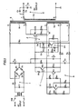
- One of power supply circuits of this type as shown in Fig. 1 is disclosed in Japanese Patent Laying-Open No. 2570/1984.
- the power supply circuit shown in Fig. 1 comprises an input rectifying portion 1, a blocking oscillation portion 2, a converter transformer 3, a fluctuation detecting portion 4, a control portion 5, an output rectifying portion 6 and a feedback current control circuit 7, and only a portion of relation to the present invention is described hereinafter.
- the conventional example shown in Fig. 1 performs a blocking oscillation, when a switching transistor TR4 is on, by letting a positive feedback current If flow from the side of a terminal e of a feedback winding N3 of the converter transformer 3 to the base of the transistor TR4 through a path shown in the figure.
- the feedback current control circuit 7 comprising a constant-current circuit CA in the current path is provided to cause the positive feedback current If to be a constant current in a steady state. More detailed description is made in this respect.
- the above positive feedback current If is caused to be a constant current for the following reason. Assuming that the feedback current control circuit 7 is not a constant-current circuit but a constant-impedance, the positive feedback current If in this case is proportional to the voltage between the terminals c and e of the feedback winding N3 and that voltage is proportional to an input voltage applied to an input winding N1. As a result, the more the input voltage applied to the input winding N1 is decreased, the more the current If is decreased. Meanwhile, referring to Fig.
- the switching transistor TR4 becomes an overdrive state when the input voltage applied to the input winding N1 is high or the load connected to the output winding N2 is increased, with the result that a stabilized control range becomes small due to any increase in power loss of the switching transistor TR4.
- the voltage of the feedback winding is also high as mentioned above, so that power consumption in the transistor TR5 is also increased.
- the positive feedback current If is always kept at a constant value while the switching transistor TR4 is on, the collector current Ii is increased linearly as time passes while the switching transistor TR4 is on and, as a result, the above current If can not be a value providing an optimum drive always during the above mentioned on period. Therefore, there is also another disadvantage that power loss of the switching transistor TR4 is originally high without regard to the state of the input voltage applied to the input winding N1 and the load connected to the output winding N2.
- a major object of the present invention is to provide a switching regulator type power supply circuit in which switching transistor means is operated in a more improved operation state without regard to an input voltage fluctuation applied to input winding of the converter transformer means and a fluctuation of a load connected to output winding, so that power loss of switching transistor means is decreased and a more stable operation with less power loss is implemented.
- the present invention comprises blocking oscillation means comprising a first switching transistor means having a common electrode, an output electrode and a control electrode, coupled to DC power supply means in series through input winding of converter transformer means and connected to positive feedback winding of the converter transformer means of the control electrode of the first switching transistor means for performing a blocking oscillating operation; positive feedback current control means coupled to the control electrode of the first switching transistor and the positive feedback winding and responsive to a voltage generated in the positive feedback winding for applying a positive feedback current increasing as a function of the lapse of time during its on period to the control electrode of the first transistor means; switching control means coupled to detecting winding of the converter transformer means and responsive to the fluctuation voltage outputted from the detecting winding and responsive to the fluctuation of the output voltage of the output winding of the converter transformer means coupled to rectify circuit means for rectifying and smoothing the output voltage for controlling the duration of the on period of the first switching transistor means.
- the positive feedback current control means comprises bias means coupled to the positive feedback winding and responsive to the voltage generated in the positive feedback winding for providing a bias voltage, a second switching transistor means having a common electrode, an output electrode and a control electrode responsive to the bias voltage for being turned on at the same time when the first switching transistor means is turned on, proportion current supply means for applying a positive feedback current increasing approximately in proportion to the lapse of time during the on period of the first switching transistor means to the control electrode of the first switching transistor means.
- the present invention comprises the converter transformer means, the blocking oscillation means including the first switching transistor means, the positive feedback current control means and the switching control means, the duration of the on period of the first switching transistor means is controlled appropriately by the switching control means at the time of occurrence of a fluctuation of the input voltage applied to the input winding or a fluctuation of the load connected to the output winding through the rectifying circuit means, and also a peak value of the positive feedback current applied to the first switching transistor means by the positive feedback current control means is increased or decreased because the positive feedback current control means provides the positive feedback current increasing as a function of the lapse of time during the on period of the first switching transistor means to the first switching transistor means.
- undesirable power loss of the first switching transistor means can be prevented because an operation of the first switching transistor means is stabilized and can be put in an operationally efficient state without regard to such fluctuations.
- the operation of the first switching transistor means is more stabilized and can be put in an operationally efficient state, so that undesirable power loss of the first switching transistor means can be reduced. Consequently, an advantage is brought about that a switching regulator type power supply circuit employing a stabilized blocking oscillating operation with less power loss, can be provided.
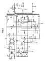
- Fig. 2 shows one example of a power supply circuit of the present invention, which is described with the same reference characters allotted to those corresponding portions used in Fig. 1.
- the blocking oscillation portion includes a series connection of the input winding N1 of the converter transformer 3 and the switching transistor TR4 interposed between the output lines L1 and L2 of the input rectifying portion 1 and is connected to a positive feedback current control circuit 8 between the feedback winding N3 of the above transformer and the base of the switching transistor TR4.
- the fluctuation detecting portion 4 is also included, which detects, by means of a transistor TR1 for detecting a fluctuation and a Zener diode D5, a fluctuation of a DC voltage between lines L3 and L4, provided by rectifying and smoothing, with a diode D6 and a capacitor C3, a voltage generated between both ends h and c of the detecting winding N4 during the off period of the switching transistor TR4.
- the control portion 5 includes a resistor R19 and a capacitor C9 connected each other at a junction K constituting an integrated circuit (IC), connected between terminals c and e of the feedback winding N3, and the control transistor TR2 connected between the base of the switching transistor TR4 and the terminal c of the feedback winding N3, that is a reference line L4, the junction K and a node point G of an output side of the fluctuation detecting portion 4 being connected to the base of the transistor TR2.
- IC integrated circuit
- the output rectifying portion 6 rectifies and smooths, with a diode D9 and a capacitor C8, a voltage generated on the output winding N2 of the converter transformer 3 when the switching transistor TR4 is off.
- the above mentioned positive feedback current control circuit 8 comprises a diode D11, a capacitor C10 and a resistor R20 connected between the terminal e of the feedback winding N3 and the base of the switching transistor TR4 as shown in Fig. 2, a series connection of an inductor L1 and a PNP type transistor TR6 connected between a junction J and the base of the switching transistor TR4, and a series connection of a Zener diode D12 and a resistor R21 connected each other at a junction H between the junction J and the terminal c of the feedback winding N3, the junction H being connected to the base of the transistor TR6.
- the present invention is characterized by such positive feedback current control circuit 8.
- the switching transistor TR4 is triggered and is turned on by a current Is flowing from the line L1 of the input rectifying portion 1 through a starting resistor R2 and the positive feedback current If is supplied from the feedback winding N3 to the base of the above transistor TR4 through the positive feedback current control circuit 8 after conducting of the switching transistor TR4, so that a blocking oscillation is performed.
- the switching transistor TR4 is controlled in the manner to be described in the following in a steady state in which such blocking oscillation is performed.
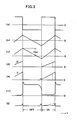
- a rectangular wave voltage shown in Fig. 2 is generated between both ends e and c of the feedback winding N3 in a steady state
- the rectangular wave voltage is integrated by the integrating circuit (IC) and a triangular wave voltage shown in Fig. 3 (b) is generated at the junction K.
- the node point G between resistors R7 and R5 connected between the collector of the fluctuation detecting transistor TR1 and the line L4 is at a positive potential corresponding to the voltage between both ends of a capacitor C3 for getting a detected voltage with respect to the line L4. Then, it follows that a potential on a node point M changes as shown in Fig. 3 (c), because the previous triangular wave voltage on the node point M is superimposed onto the positive potential.
- the transistor TR2 when the potential of the point M is higher than the reference voltage of the line L3 by more than a threshold voltage Vbe between the base and emitter of the control transistor TR2, the transistor TR2 is turned on. Then, it follows that the positive feedback current If from the feedback winding N3 is bypassed by the control transistor TR2, so that the switching transistor TR4 is turned off. Then, the switching transistor TR4 becomes on state by a normal blocking oscillating operation after a predetermined period of time from the turn off.
- the switching transistor TR4 repeats the on and off operation hereafter and, as a result, a voltage generated on the output winding N2 is rectified and smoothed by means of the diode D9 and the capacitor C8 to provide a DC output voltage.
- the DC output voltage fluctuates
- the DC voltage from the fluctuation detecting winding N4 by means of the diode D6 and the capacitor C3 also changes accordingly and a potential at the point G also changes and, as a result, a turn-off timing of the switching transistor TR4, that is, the length of the on period can be controlled such that the DC output voltage is increased, the length of the on period is decreased corresponding to a potential change of the point G and then the DC output voltage is stabilized.
- the positive feedback current of the switching transistor TR4 becomes the above mentioned current If substantially and that the positive feedback current If is increased during the on period of the switching transistor TR4, as shown in Fig. 3(d).
- the on period is reduced like a dashed line in Fig. 3(d) due to, for example, an increase of the input voltage or a decrease of the load and a peak value of the collector current Ii (Fig. 3(e)) of the switching transistor TR4 is decreased, the switching transistor TR4 never becomes a overdrive state because a peak value of the positive feedback current If is decreased accordingly.
- a peak value of the positive feedback current If is increased in proportion to the on period of the TR4 and, as a result, an underdrive state of the switching transistor TR4 can be prevented. Since the above mentioned positive feedback current If varies with the collector current Ii of the switching transistor TR4, that current If can be set to be in an optimum drive state for the collector current Ii at each moment over approximate all period of the on period.
- Fig. 3(f) shows a voltage between the collector and the emitter of the switching transistor TR4 and Fig. 3(g) shows a power loss of that transistor TR4, a dashed line showing the conventional one.
- the diode D11, capacitor C10 and the resistor R20 in the positive feedback current control circuit 8 become necessitated immediately after the power supply switch SW is turned on. This means that an enough voltage to turn on the Zener diode D12 is not generated on the feedback winding N3 immediately after that turning on and, therefore, a current flowing through the capacitor C10 and the diode D11 is applied to the base of the switching transistor TR4 through the resistor R20 because the transistor TR6 is off.
- Fig. 4 shows another embodiment of the present invention in which the transistor TR6 in the positive feedback current control circuit 8 is of a PNP type. Since an operation is the same as that in Fig. 2, its description is omitted and the same reference characters are allotted to the same or corresponding portions.
- the present invention is not limited to the above mentioned embodiment, insofar as the present invention comprises a switching power supply circuit of a blocking oscillation type irrespective of a type of turn-off control for the switching transistor TR4 and, therefore, the present invention is applicable to even a case when a control circuit for turning off comprises the conventional or still other structure.
- the present invention comprises the blocking oscillation means including a series connection of the input winding of the converter transformer means and the first switching transistor means connected to the DC power supply means for a blocking oscillating operation; the positive feedback current control means for receiving a voltage generated in the positive feedback winding of the converter transformer means and for applying to the control electrode of the first switching transistor means a positive feedback current increasing as a function of the lapse of time during the on period of the first switching transistor means; and switching control means responsive to a voltage provided from detecting winding for detecting a fluctuation of the output voltage of the output winding of the converter transformer means due to a fluctuation of a load for controlling the length of the on period of the first switching transistor means.
- the length of the on period of the first switching transistor is controlled by the switching control means and positive feedback current increasing as a function of the lapse of time during the on period of the first switching transistor means is applied to the control electrode of the first switching transistor means. Therefore, it is possible to perform an operation of the first switching transistor means in a stable and efficient manner with less power loss to fluctuations of the load and the input voltage and, as a result, a switching regulator type power supply circuit using a stabilized and efficient blocking oscillation is provided.
Landscapes
- Engineering & Computer Science (AREA)
- Power Engineering (AREA)
- Dc-Dc Converters (AREA)
Applications Claiming Priority (2)
| Application Number | Priority Date | Filing Date | Title |
|---|---|---|---|
| JP61216517A JPH0728533B2 (ja) | 1986-09-12 | 1986-09-12 | スイツチング制御型電源回路 |
| JP216517/86 | 1986-09-12 |
Publications (3)
| Publication Number | Publication Date |
|---|---|
| EP0259889A2 true EP0259889A2 (de) | 1988-03-16 |
| EP0259889A3 EP0259889A3 (en) | 1989-06-14 |
| EP0259889B1 EP0259889B1 (de) | 1992-04-08 |
Family
ID=16689674
Family Applications (1)
| Application Number | Title | Priority Date | Filing Date |
|---|---|---|---|
| EP87113345A Expired - Lifetime EP0259889B1 (de) | 1986-09-12 | 1987-09-11 | Geregeltes Schaltnetzteil |
Country Status (5)
| Country | Link |
|---|---|
| US (1) | US4802076A (de) |
| EP (1) | EP0259889B1 (de) |
| JP (1) | JPH0728533B2 (de) |
| KR (1) | KR920008204B1 (de) |
| DE (1) | DE3778100D1 (de) |
Cited By (2)
| Publication number | Priority date | Publication date | Assignee | Title |
|---|---|---|---|---|
| WO1998011659A1 (en) * | 1996-09-12 | 1998-03-19 | Thomson Consumer Electronics, Inc. | Self oscillating proportional drive zero voltage switching power supply |
| US5877946A (en) * | 1996-09-12 | 1999-03-02 | Thomson Consumer Electronics, Inc. | Forward converter with an inductor coupled to a transformer winding |
Families Citing this family (8)
| Publication number | Priority date | Publication date | Assignee | Title |
|---|---|---|---|---|
| EP0398722A3 (de) * | 1989-05-18 | 1991-01-30 | Hirotami Nakano | Unterbrechungsfreie Stromversorgungseinrichtung und Isolationsverfahren |
| KR0184568B1 (ko) * | 1996-04-25 | 1999-05-15 | 김광호 | 에스엠피에스의 이상 전원 보호장치 |
| DE19619751A1 (de) * | 1996-05-15 | 1997-11-20 | Thomson Brandt Gmbh | Schaltnetzteil |
| JP3351464B2 (ja) * | 1998-02-13 | 2002-11-25 | 株式会社村田製作所 | 自励発振型スイッチング電源装置 |
| JP3527636B2 (ja) * | 1998-06-12 | 2004-05-17 | 松下電工株式会社 | 自励型dc−dcコンバータ |
| KR100577435B1 (ko) * | 1999-02-13 | 2006-05-08 | 삼성전자주식회사 | 스위칭 모드 전원 공급장치의 전원 안정화회로 |
| US9006624B2 (en) * | 2010-07-22 | 2015-04-14 | General Electric Company | Resonant frequency detection for induction resonant inverter |
| JP6939203B2 (ja) * | 2017-07-28 | 2021-09-22 | スミダコーポレーション株式会社 | 循環電流低減回路、トランスユニット |
Family Cites Families (7)
| Publication number | Priority date | Publication date | Assignee | Title |
|---|---|---|---|---|
| US4447866A (en) * | 1979-06-14 | 1984-05-08 | Conver Corporation | Supplement to cross regulation in DC to DC converters |
| JPS5936151Y2 (ja) * | 1979-09-18 | 1984-10-05 | シャープ株式会社 | 電源回路 |
| US4370701A (en) * | 1981-04-24 | 1983-01-25 | Rockwell International Corporation | Energy conserving drive circuit for switched mode converter utilizing current snubber apparatus |
| JPS592570A (ja) * | 1982-06-25 | 1984-01-09 | Sanyo Electric Co Ltd | スイツチング制御型電源回路 |
| US4488210A (en) * | 1982-04-07 | 1984-12-11 | Sanyo Electric Co., Ltd. | Power supply circuit of switching regulator type |
| DE3568673D1 (en) * | 1984-07-20 | 1989-04-13 | Sanyo Electric Co | Power supply circuit of switching regulator type |
| US4654772A (en) * | 1986-03-06 | 1987-03-31 | Fyrnetics, Inc. | Power supply for electrostatic air cleaner |
-
1986
- 1986-09-12 JP JP61216517A patent/JPH0728533B2/ja not_active Expired - Lifetime
-
1987
- 1987-09-03 US US07/092,820 patent/US4802076A/en not_active Expired - Lifetime
- 1987-09-11 KR KR1019870010077A patent/KR920008204B1/ko not_active Expired
- 1987-09-11 DE DE8787113345T patent/DE3778100D1/de not_active Expired - Lifetime
- 1987-09-11 EP EP87113345A patent/EP0259889B1/de not_active Expired - Lifetime
Cited By (2)
| Publication number | Priority date | Publication date | Assignee | Title |
|---|---|---|---|---|
| WO1998011659A1 (en) * | 1996-09-12 | 1998-03-19 | Thomson Consumer Electronics, Inc. | Self oscillating proportional drive zero voltage switching power supply |
| US5877946A (en) * | 1996-09-12 | 1999-03-02 | Thomson Consumer Electronics, Inc. | Forward converter with an inductor coupled to a transformer winding |
Also Published As
| Publication number | Publication date |
|---|---|
| JPS6373877A (ja) | 1988-04-04 |
| EP0259889A3 (en) | 1989-06-14 |
| DE3778100D1 (de) | 1992-05-14 |
| KR880004630A (ko) | 1988-06-07 |
| US4802076A (en) | 1989-01-31 |
| EP0259889B1 (de) | 1992-04-08 |
| JPH0728533B2 (ja) | 1995-03-29 |
| KR920008204B1 (ko) | 1992-09-25 |
Similar Documents
| Publication | Publication Date | Title |
|---|---|---|
| US5019955A (en) | DC-to-AC voltage converter having galvanically separate input and output circuits | |
| US6690586B2 (en) | Switching power source device | |
| US6295211B1 (en) | Switching power supply unit having delay circuit for reducing switching frequency | |
| US4945465A (en) | Switched-mode power supply circuit | |
| US6285566B1 (en) | RCC power supply with remote disabling of oscillation frequency control | |
| US4208705A (en) | Switching regulated power supply apparatus | |
| US4802076A (en) | Switching regulator type power supply circuit | |
| EP0038200A1 (de) | Leistungsstromversorgungsschaltung der schaltungsgeregelten Art | |
| US6532159B2 (en) | Switching power supply unit | |
| US5943222A (en) | Self-excited RCC type switching power supply apparatus | |
| US4488210A (en) | Power supply circuit of switching regulator type | |
| US5389871A (en) | Self-oscillation type DC-DC converter | |
| US6016259A (en) | Power supply circuit | |
| EP0935333A2 (de) | Schaltnetzteil | |
| EP0091133B1 (de) | Energieversorgungsschaltung des Schaltreglertyps | |
| CA2214217C (en) | Switching power supply apparatus | |
| US4176302A (en) | Vertical deflection output circuit | |
| JPH0315423B2 (de) | ||
| JPH0747992Y2 (ja) | スイッチングレギュレータ | |
| JPH10108462A (ja) | 自励式スイッチング電源回路 | |
| JP2003309972A (ja) | 自励式スイッチング電源 | |
| KR840002469B1 (ko) | 쵸퍼형 자동변환 전원회로 | |
| JPH0880041A (ja) | スイッチング電源装置 | |
| JPS6366154B2 (de) | ||
| JPS5822581A (ja) | 自励式コンバ−タ回路 |
Legal Events
| Date | Code | Title | Description |
|---|---|---|---|
| PUAI | Public reference made under article 153(3) epc to a published international application that has entered the european phase |
Free format text: ORIGINAL CODE: 0009012 |
|
| AK | Designated contracting states |
Kind code of ref document: A2 Designated state(s): DE FR GB |
|
| PUAL | Search report despatched |
Free format text: ORIGINAL CODE: 0009013 |
|
| AK | Designated contracting states |
Kind code of ref document: A3 Designated state(s): DE FR GB |
|
| 17P | Request for examination filed |
Effective date: 19890529 |
|
| 17Q | First examination report despatched |
Effective date: 19910220 |
|
| GRAA | (expected) grant |
Free format text: ORIGINAL CODE: 0009210 |
|
| AK | Designated contracting states |
Kind code of ref document: B1 Designated state(s): DE FR GB |
|
| REF | Corresponds to: |
Ref document number: 3778100 Country of ref document: DE Date of ref document: 19920514 |
|
| ET | Fr: translation filed | ||
| PLBE | No opposition filed within time limit |
Free format text: ORIGINAL CODE: 0009261 |
|
| STAA | Information on the status of an ep patent application or granted ep patent |
Free format text: STATUS: NO OPPOSITION FILED WITHIN TIME LIMIT |
|
| 26N | No opposition filed | ||
| REG | Reference to a national code |
Ref country code: GB Ref legal event code: IF02 |
|
| PGFP | Annual fee paid to national office [announced via postgrant information from national office to epo] |
Ref country code: GB Payment date: 20060906 Year of fee payment: 20 |
|
| PGFP | Annual fee paid to national office [announced via postgrant information from national office to epo] |
Ref country code: DE Payment date: 20060907 Year of fee payment: 20 |
|
| PGFP | Annual fee paid to national office [announced via postgrant information from national office to epo] |
Ref country code: FR Payment date: 20060908 Year of fee payment: 20 |
|
| REG | Reference to a national code |
Ref country code: GB Ref legal event code: PE20 |
|
| PG25 | Lapsed in a contracting state [announced via postgrant information from national office to epo] |
Ref country code: GB Free format text: LAPSE BECAUSE OF EXPIRATION OF PROTECTION Effective date: 20070910 |