EP0935333A2 - Schaltnetzteil - Google Patents
Schaltnetzteil Download PDFInfo
- Publication number
- EP0935333A2 EP0935333A2 EP99102313A EP99102313A EP0935333A2 EP 0935333 A2 EP0935333 A2 EP 0935333A2 EP 99102313 A EP99102313 A EP 99102313A EP 99102313 A EP99102313 A EP 99102313A EP 0935333 A2 EP0935333 A2 EP 0935333A2
- Authority
- EP
- European Patent Office
- Prior art keywords
- switching element
- voltage
- transistor
- switching
- winding
- Prior art date
- Legal status (The legal status is an assumption and is not a legal conclusion. Google has not performed a legal analysis and makes no representation as to the accuracy of the status listed.)
- Withdrawn
Links
- 238000004804 winding Methods 0.000 claims abstract 36
- 239000003990 capacitor Substances 0.000 claims 4
- 238000000034 method Methods 0.000 claims 3
- 230000008878 coupling Effects 0.000 claims 1
- 238000010168 coupling process Methods 0.000 claims 1
- 238000005859 coupling reaction Methods 0.000 claims 1
Images


Classifications
-
- H—ELECTRICITY
- H02—GENERATION; CONVERSION OR DISTRIBUTION OF ELECTRIC POWER
- H02M—APPARATUS FOR CONVERSION BETWEEN AC AND AC, BETWEEN AC AND DC, OR BETWEEN DC AND DC, AND FOR USE WITH MAINS OR SIMILAR POWER SUPPLY SYSTEMS; CONVERSION OF DC OR AC INPUT POWER INTO SURGE OUTPUT POWER; CONTROL OR REGULATION THEREOF
- H02M3/00—Conversion of DC power input into DC power output
- H02M3/22—Conversion of DC power input into DC power output with intermediate conversion into AC
- H02M3/24—Conversion of DC power input into DC power output with intermediate conversion into AC by static converters
- H02M3/28—Conversion of DC power input into DC power output with intermediate conversion into AC by static converters using discharge tubes with control electrode or semiconductor devices with control electrode to produce the intermediate AC
- H02M3/325—Conversion of DC power input into DC power output with intermediate conversion into AC by static converters using discharge tubes with control electrode or semiconductor devices with control electrode to produce the intermediate AC using devices of a triode or a transistor type requiring continuous application of a control signal
- H02M3/335—Conversion of DC power input into DC power output with intermediate conversion into AC by static converters using discharge tubes with control electrode or semiconductor devices with control electrode to produce the intermediate AC using devices of a triode or a transistor type requiring continuous application of a control signal using semiconductor devices only
- H02M3/33507—Conversion of DC power input into DC power output with intermediate conversion into AC by static converters using discharge tubes with control electrode or semiconductor devices with control electrode to produce the intermediate AC using devices of a triode or a transistor type requiring continuous application of a control signal using semiconductor devices only with automatic control of the output voltage or current, e.g. flyback converters
- H02M3/33523—Conversion of DC power input into DC power output with intermediate conversion into AC by static converters using discharge tubes with control electrode or semiconductor devices with control electrode to produce the intermediate AC using devices of a triode or a transistor type requiring continuous application of a control signal using semiconductor devices only with automatic control of the output voltage or current, e.g. flyback converters with galvanic isolation between input and output of both the power stage and the feedback loop
Definitions
- the present invention relates to a switching power supply apparatus, more particularly, it concerns a switching power supply apparatus using the RCC (Ringing Choke Converter) system.
- RCC Ringing Choke Converter
- a switching power supply apparatus comprising an RCC system which is relatively simple in structure and highly efficient is extensively used to supply the stable DC voltage from the commercial AC power source.
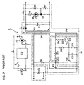
- FIG. 7 illustrates a switching power supply apparatus of the conventional RCC system.
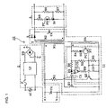
- a switching power supply apparatus 1 comprises an input circuit 2, a DC-DC converter circuit 3, a voltage detection circuit 4, and a control circuit 5.
- the input circuit 2 comprises a diode bridge DB for rectification, a fuse F and line filter LF provided between the AC power source and an input end of the diode bridge DB, and a smoothing capacitor C1 provided in parallel to an output end of the diode bridge DB.
- the DC-DC converter circuit 3 comprises a transformer T having a primary winding N1, a secondary winding N2 of opposite polarity to the primary winding N1 and a feedback winding Nb of the same polarity as the primary winding N1, a switching element FET Q1 connected in series with the primary winding N1, a starting resistor R1 connected between one end of the primary winding N1 and the gate control terminal of the FET Q1, a diode D1 for rectification connected in series with the secondary winding N2, and a smoothing capacitor C4 connected between a cathode of the diode D1 and one end of the secondary winding N2.
- the voltage detection circuit 4 provided on the output side of the DC-DC converter circuit 3 comprises a resistor R5, a light-emitting diode PD on the light emission side of a photo coupler PC, a shunt regulator Sr, and resistors R6,R7.
- the resistor R5, the light-emitting diode PD, and the shunt regulator Sr are connected in series, and provided in parallel to the capacitor C4 of the DC-DC converter circuit 3.
- the resistors R6 and R7 are also connected in series, and provided in parallel to the capacitor C4.
- a common connection of the resistor R6 to the resistor R7 is connected to the control terminal of the shunt regulator Sr.
- the control circuit 5 comprises a resistor Rb and a capacitor C3 connected in series between one end of the feedback winding Nb and a gate of the FET QQe FET Q1, a transistor Q2 connected between the gate of the FET Q1 and the other end of the feedback winding Nb, a resistor R2 connected between one end of the feedback winding Nb and a base of the transistor Q2, a resistor R3 and a capacitor C2 connected in parallel between the base and emitter of the transistor Q2, a resistor R4 connected in series between one end of the feedback winding Nb and the base of the transistor Q2, the diode D2 and a photo-transistor PT on the light reception side of the photo coupler PC.
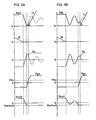
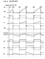
- Vgs denotes the voltage between the gate and source of the FET Q1
- V1 denotes the voltage to be applied to the primary winding N1
- I1 denotes the current flowing in the primary winding N1
- Vds denotes the voltage between the drain and source of the
- Vbe2 denotes the voltage between the base and emitter of the transistor Q2
- Vb denotes the voltage generated in the feedback winding Nb
- V2 denotes the voltage generated in the secondary winding N2
- I2 denotes the current flowing in the secondary winding N2.
- ON and OFF indicated at the upper part of the graph indicate the timing at which FET Q1 is turned from OFF to ON (hereinafter, referred to as "turn-ON”), and the timing at which the FET Q1 is turned from ON to OFF (hereinafter, referred to as "turn-OFF”), respectively.
- the FET Q1 is in the OFF condition, and no current I1 flows in the primary winding N1, but current flows in the internal capacitance formed between the gate and the source of the FET Q1 through the starting resistor R1.
- the voltage Vgs between the gate and the source of the FET Q1 is increased, and the FET Q1 starts to turn ON at the time exceeding the threshold of the FET Q1.
- the FET Q1 When the FET Q1 starts to turn ON, the voltage Vds between the drain and the source of the FET Q1 becomes approximately 0V, the input voltage is applied to the primary winding N1 of the transformer T, the current I1 starts to flow, and the voltages Vb and V2 are generated in the feedback winding Nb and the secondary winding N2.
- the current flows into the gate of FET Q1 from the feedback winding Nb through the resistor Rb and the capacitor C3.
- the voltage Vb generated in the feedback winding Nb the increase of the voltage Vgs between the gate and the source of the FET Q1 is accelerated, and FET Q1 is completely turned ON.
- the voltage V2 generated in the secondary winding N2 is the voltage reverse to the diode D1 for rectification, and no current I2 flows in the secondary winding N2.
- the capacitor C2 When FET Q1 is turned ON and the voltage Vb of positive polarity is generated in the feedback winding Nb, the capacitor C2 is charged through the resistor R2, a resistor R4, a diode D4 and the photo-transistor PT which are described below, and the voltage across the capacitor C2, that is, the voltage Vbe2 between the base and the emitter of the transistor Q2 is increased.
- the charging speed (the time constant) is determined by the values of the resistors R2,R3,R4 and the capacitor C2 and the photo-transistor PT.
- the transistor Q2 When the voltage Vbe2 between the base and the emitter of the transistor Q2 is increased, and exceeds the forward voltage Vbe(on) 2 between the base and the emitter of the transistor Q2, the transistor Q2 is turned ON.
- the transistor Q2 When the transistor Q2 is turned ON, the voltage between the collector and the emitter of the transistor Q2, that is, the voltage Vgs between the gate and the source of FET Q1is approximately 0
- the voltage V1 to be applied to the primary winding N1 is 0V, and the flowing current I1 is also 0.
- a voltage of negative polarity is generated in the primary winding N1, the secondary winding N2, and the feedback winding Nb.
- a voltage of n-times (the turn ratio of the primary winding to the secondary winding) the voltage V2 of negative polarity generated in the secondary winding is generated in the primary winding.
- the voltage Vb of negative polarity generated in the feedback winding Nb rapidly absorbs the charge from the internal capacitance formed between the gate and the source of the FET Q1 through the capacitor C3 and the resistor Rb, and the FET Q1 is completely turned off.
- the charge accumulated in the capacitor C2 is also absorbed through the resistor R2, a the reverse voltage is applied to the capacitor C2, and the capacitor C2 is further charged in the reverse direction, the voltage Vbe2 between the base and the emitter of the transistor Q2 is biased negative, and the transistor Q2 is turned OFF.
- the transistor Q2 is instantaneously turned ON only when it turns off the FET Q1.
- the current I2 flowing in the secondary winding N2 when the FET Q1 is turned OFF, is gradually reduced as the magnetic energy from the transformer T is released, and finally becomes 0.
- the voltages V2 and Vb generated in the secondary winding N2 and the feedback winding Nb tend to be attenuated in an oscillating manner with 0V on the boundary if they are left as they are.
- the voltage which is temporarily changed from the negative polarity to the positive polarity in the feedback winding Nb, is referred to as the "kick voltage".
- the current flows from the feedback winding Nb into the internal capacitance formed between the gate and the source of the FET Q1 through the resistor Rb and the capacitor C3, and the voltage Vgs between the gate and the source of the FET Q1 is increased.
- the kick voltage is not less than the prescribed value, the voltage Vgs between the gate and the source exceeds the threshold, and the FET Q1 is turned on. Because the starting resistor R1 is set to a large value, the current flowing through it is small, and it does not cause the FET Q1 to be turned on by the current flowing in the starting resistor R1 like starting.
- the voltages V2 and Vb generated in the secondary winding N2 and the feedback winding Nb are forcibly increased to the positive polarity, and the oscillation of the voltage is forcibly terminated.
- the FET Q1 is repeatedly turned on and turned off to be operated as the switching power supply apparatus.
- the output voltage is split by two resistors R6 and R7 for detection, and inputted in the shunt regulator Sr.
- the shunt regulator Sr compares the inputted voltage with the internal reference voltage, and causes a current to flow according to the difference.
- the load (not shown in the figure) to be connected to the switching power supply apparatus 1 is decreased, and the output voltage is increased, the voltage at the connection part of the resistor R6 to the resistor R7 is also increased, the input voltage to the shunt regulator Sr is increased to allow more current to flow.
- the current flowing in the shunt regulator Sr is increased, the current flowing in the light-emitting diode PD of the photo coupler PC connected thereto in series is also increased, and the quantity of light emitted from the light-emitting diode PD is increased.
- the quantity of light emitted from the light-emitting diode PD is increased, the current flowing in the photo-transistor PT of the photo coupler PC connected to the control circuit 5 is also increased.
- the current flowing in the photo-transistor PT is the current to charge the capacitor C2 together with the current flowing in the resistor R2 when the voltage Vb generated in the feedback winding Nb is of the positive polarity as described above, and when the current flowing in the photo-transistor PT is increased, the time to charge the capacitor C2 is shortened.
- the time until the transistor Q2 is turned ON is shortened, and the time until the FET Q1 is turned off, that is, the time while the FET Q1 is ON is shortened.
- the time while the FET Q1 is ON is short, the magnetic energy accumulated in the transformer T is also smaller, the voltage V2 generated in the secondary winding N2 is also dropped, and the output voltage is reduced. Because the time while the FET Q1 is OFF is shortened proportional to the time while the FET Q1 is ON, the switching frequency of the switching power supply apparatus 1 is increased by the shortening of the time while the FET Q1 is ON and OFF.
- the switching loss is generated whenever the FET Q1 is turned on and turned off, the magnitude of the switching loss affects the efficiency of the switching power supply apparatus 1. Also, because the total switching loss during the prescribed period is proportional to the switching number of the , the switching frequency also affects the efficiency of the switching power supply apparatus 1.
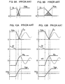
- FIGs. 9A and 9B indicate the time change of the voltage Vds between the drain and the source of the FET Q1 during the turn-OFF and the current I1 flowing therein on an expanded time scale.
- FIGs. 10A and 10B show the time change of the voltage Vds between the drain and the source of the FET Q1 during the turn-ON and the current I1 flowing therein, the current I2 flowing in the secondary winding N2, the voltage Vb generated in the feedback winding Nb, and the voltage Vgs between the gate and the source of the FET Q1 in the expanded time scale.
- the area of the hatched part is reduced so as to reduce the switching loss, and for this purpose, the turn-off speed of the FET Q1 is increased.
- This can be achieved by reducing the resistance of the resistor Rb as much as possible so as to easily allow current directed from the gate of the FET Q1 to the feedback winding Nb to flow.
- the resistance of the resistor Rb is increased, the turn-off speed is reduced, the voltage is applied between the drain and the source of the FET Q1 as indicated in FIG. 9B, the current-flowing time is increased, and the area of the hatched part, that is, the switching loss is increased.
- the operation is started from the time point when the current I2 flowing in the secondary winding N2 is 0.
- the voltage V2 (not shown in the figure) generated in the secondary winding N2
- the voltage Vb generated in the feedback winding Nb and the voltage Vds between the drain and the source of the FET Q1 are attenuated in an oscillating manner as indicated by the dotted line, reaching to a certain value.
- the voltage Vb of the feedback winding Nb is temporarily changed from the negative polarity to the positive polarity and turned into the kick voltage, and the current flowing in the feedback winding Nb flows into the gate of the FET Q1 through the resistor Rb and the capacitor C3.
- the FET Q1 is turned on.
- the turn-on speed of the FET Q1 is large, the current I1 starts to flow before the voltage Vds between the drain and the source of the FET Q1 has not sufficiently dropped.
- the turn-on time of the FET Q1 can be delayed to some degree, and for this purpose, the current from the feedback winding Nb to the gate of the FET Q1 through the resistor Rb and the capacitor C3 is difficult to cause to flow by increasing the resistance of the resistor Rb to some degree.
- 10B indicates the timing when the resistance of the resistor Rb is increased to some degree, and because the time that the voltage Vgs between the gate and the source of the FET Q1 reaches the threshold is long, the FET Q1 is turned on after the voltage Vds between the drain and the source of the FET Q1 has sufficiently dropped, the time of generating the switching loss is shortened, and the voltage Vds between the drain and the source of the FET Q1 is also dropped.
- the resistance of the resistor Rb is required to be small, while, to reduce the switching loss during the turn-on, the resistance of the resistor Rb is required to be large.
- the resistance of the resistor Rb is in a conflicting relationship between the turn-on and the turn-off, and required to be set to an appropriate value in a balanced manner, and in any case, this has been a difficult problem in reducing the switching loss.
- the switching power supply apparatus of an RCC system is characterized in that the switching frequency is increased as the load is decreased, and there is a problem that the switching loss is increased for a particularly small load because the switching loss is proportional to the switching frequency.
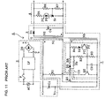
- FIG. 11 The basic structure of the switching power supply apparatus illustrated in FIG. 11 is disclosed in Japanese Unexamined Patent Publication No. 8-80041.
- the same symbol is attached to the part same as or equivalent to the part in FIG. 7, and its explanation is omitted.
- the difference from the switching power supply apparatus 1 in FIG. 7 is that the diode D3 and a resistor R8 which are connected to each other in series, are connected in parallel to the resistor Rb in the control circuit 7.
- the anode of the diode D3 is connected to the gate side of the FET Q1 and the cathode is connected toward one end side of the feedback winding Nb.
- the turn-on time is dependent only on the resistance of the resistor Rb, and the turn-on timing of the FET Q1 is delayed, that means, reduction of the switching frequency is limited.
- the FET Q1 is required to be rapidly turned on after the FET Q1 is started to be turned ON, but it takes long before the turn-on time of the FET Q1 if the resistance of the resistor Rb is excessively increased, and the switching loss is increased all the more.
- the switching power supply apparatus of the present invention comprises: a transformer having a primary winding, a secondary winding and a feedback winding, a switching element connected in series to the primary winding, a control circuit provided between a control terminal of the switching element and the feedback winding, a rectifying circuit connected to the secondary winding, further wherein a control element is provided between the control terminal of the switching element and the feedback winding, and a delay circuit being connected to a control terminal of the control element.
- a resistor may be provided in parallel to the control element.
- the control element may comprise a PNP transistor in which a base is the control terminal, an emitter is connected to one end of the feedback winding, a collector is connected to the control terminal of the switching element, and the delay circuit may comprise a capacitor connected between the emitter and the base of the transistor and a resistor connected between the base of the transistor and the other end of the feedback winding.
- control element may comprise an NPN transistor in which a base is the control terminal, a collector is connected to one end of the feedback winding, an emitter is connected to the control terminal of the switching element, and the delay circuit may comprise a capacitor connected between the emitter and the base of the transistor and a resistor connected between the collector and the base of the transistor.
- the turn-on timing of the switching element is delayed by separating the current flow between the control terminal of the switching element and the feedback winding for the turn-on and for the turn-off of the switching element, and delaying the timing when the current due to the kick voltage flows in the control terminal of the switching element by the control element and the delay circuit during the turn-on, while the switching loss can be reduced by easily causing the current to flow from the control terminal of the switching element to the feedback winding to reduce the turn-off time during the turn-on.
- the turn-on timing of the switching element by delaying the turn-on timing of the switching element, the increase of the switching frequency can be suppressed, and the switching loss can also be reduced thereby.
- the turn-on delay time of the switching element is shortened and the switching loss is further reduced by connecting a resistor of large resistance to the control element in parallel.
- FIG. 1 is a block diagram illustrating one embodiment of a switching power supply apparatus of the present invention.
- FIGs. 2A and 2B are graphs of the time change of the voltage and the current of each part when the switching power supply apparatus in FIG. 1 is turned on.
- FIG. 3 is a graph illustrating the relationship between the output voltage and the switching frequency of the switching power supply apparatus in FIG. 1.
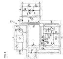
- FIG. 4 is a block diagram illustrating another embodiment of the switching power supply apparatus of the present invention.
- FIG. 5 is a block diagram illustrating still another embodiment of the switching power supply apparatus of the present invention.
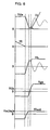
- FIG. 6 is a graph of the time change of the voltage and the current of each part when the switching power supply apparatus in FIG. 5 is turned on.
- FIG. 7 is a block diagram illustrating a conventional switching power supply apparatus.
- FIG. 8 is a graph of the time change of the voltage and the current of each part of the switching power supply apparatus in FIG. 7.
- FIGs. 9A and 9B are graphs of the time change of the voltage and the current to be applied to a switching element when the switching power supply apparatus in FIG. 7 is turned off.
- FIGs. 10A and 10B are graphs of the time change of the voltage and the current of each part when the switching power supply apparatus in FIG. 7 is turned on.
- FIG. 11 is a block diagram illustrating another conventional switching power supply apparatus.
- a control element Q3 is provided in place of a resistor RB.
- the control element Q3 may be a bipolar transistor, e.g., a PNP transistor whose emitter is connected to one end of the feedback winding Nb and whose collector is connected to an anode of a diode D3.
- a resistor R9 is connected between the base which is a control terminal of the transistor Q3 and the other end of the feedback winding Nb, and a capacitor C5 is connected between the base and the emitter of the transistor Q3.
- the capacitor C5 and the resistor R9 constitute a delay circuit.
- the resistance of a resistor R8 is set to a smaller value similar to that of the resistor R8 in the switching power supply apparatus 6 in FIG. 11.
- the current I1 starts to flow after the voltage Vds between the drain and the source of the FET Q1 drops to some degree by the current flowing from the feedback winding Nb due to the kick voltage generated in the feedback winding Nb in a delayed manner for the prescribed time by the delay circuit comprising the capacitor C5 and the resistor R9 and the transistor Q3 which is the control element.
- the operation of the delay circuit comprising capacitor C5 and resistor R9 coupled to the transistor Q3 is explained using the respective time changes of the voltage Vds between the drain and the source of the FET Q1 during the turn-on indicated in FIGs. 2A and 2B and the current I1 flowing therein, the current I2 flowing in the secondary winding N2, the voltage Vb generated in the feedback winding Nb, the voltage Vgs between the gate and the source of the , and the voltage Vbe3 between the base and the emitter of the transistor Q3.
- the voltage V2 generated in the secondary winding N2 (not shown in the figure), the voltage Vb generated in the feedback winding Nb, and the voltage Vds between the drain and the source of the FET Q1 are attenuated to be a certain value in an oscillating manner as indicated by the dotted line.
- the voltage Vb generated in the feedback winding Nb is temporarily changed from the negative polarity to the positive polarity and becomes the kick voltage, and the current flowing from the feedback winding Nb is first returned to the feedback winding Nb through the capacitor C5 and the resistor R9, and does not flow into the base of the .
- the voltage Vbe3 between the base and the emitter of the transistor Q3, that is, the voltage across the capacitor C5 is changed to approximately 0V from the reverse-biased condition, while the transistor Q3 is still left in the OFF condition.
- the voltage Vbe3 between the base and the emitter of the transistor Q3 is biased negative, and reaches the forward voltage Vbe(on)3 between the base and the emitter.
- the transistor Q3 When the voltage Vbe3 between the base and the emitter reaches the forward voltage Vbe(on) 3 between the base and the emitter, the transistor Q3 is turned ON, the current abruptly flows in the gate of the FET Q1 between the emitter and the collector of the transistor Q3 from the feedback winding Nb by the kick voltage generated in the feedback winding Nb, and the voltage Vgs between the gate and the source of the FET Q1 exceeds the threshold Vth and the FET Q1 is turned on.
- the turn-on timing of the FET Q1 can be appropriately delayed by combining the transistor Q3 which is the control element with the capacitor C5 and the resistor R9 to constitute the delay circuit, and the transition time from OFF to ON can be left short.
- the voltage between the drain and the source when the current starts to flow in the FET Q1 is reduced to some degree compared with the conventional value, the voltage is applied between the drain and the source, the time when the current flows is shortened, and generation of the switching loss can be reduced.
- FIG. 3 shows the relationship between the output power of the switching power supply apparatus 10 and the switching frequency.
- xl indicates the characteristic of the conventional switching power supply apparatus 1
- x2 indicates the characteristic of the switching power supply apparatus 10 of the present invention.
- the switching frequency is rapidly increased as the output power is reduced (that is, the load is decreased) in the conventional switching power supply apparatus 1, while the increase of the switching frequency is suppressed in the switching power supply apparatus 10 of the present invention, and large fluctuation in the switching frequency is eliminated from a heavy load to the small load.
- the switching loss in the small load can be reduced in the switching power supply apparatus of the present invention.
- the turn-on timing of the FET Q1 can be further delayed by further increasing the time constant of the delay circuit while the transition time from OFF to ON of the FET Q1 is left unchanged. In this case, the increase of the switching frequency can be further suppressed, and the switching loss can be further reduced.
- a protective resistor may be connected in series to the emitter of the transistor Q2 though it is omitted in the embodiment in FIG. 1.
- the PNP transistor Q3 is used as the control element, and similar effect can be obtained by using a J-FET or MOS-FET of the P-channel type in which the source is connected to the feedback winding Nb side, and the drain is connected to the drain side of the . More particularly, when a MOS-FET is used, the cost can be reduced by omitting the diode D3 and the resistor R8 to reduce the number of parts because of the intrinsic diode characteristic from the drain to the source.
- FIG. 4 Another embodiment of the switching power supply apparatus of the present invention is illustrated in FIG. 4.
- the same symbol is attached to each part that is the same as or equivalent to a part in FIG. 1, and its explanation is omitted.
- the difference from the switching power supply apparatus 10 in FIG. 1, is that a resistor R10 is connected in parallel between the collector and the emitter of the transistor Q3 which is the control element in a control circuit 21.
- the resistance of the resistor R10 is set to be a larger value than the resistance of the resistor Rb of the conventional switching power supply apparatus 6 of FIG. 11.
- the values of the resistor R10 and of the capacitor C5 and the resistor R9 comprising the delay circuit are set so that the voltage Vgs between the gate and the source of the FET Q1 reaches the threshold immediately before the voltage Vbe3 between the base and the emitter of the transistor Q3 reaches the forward voltage Vbe(on)3 between the base and the emitter.
- the operation during the turn-on of the FET Q1 is same as that of the conventional switching power supply apparatus 6 in FIG. 11 until the voltage Vgs between the gate and the source of the FET Q1 is increased and reaches the threshold.
- the current I1 starts to flow in the primary winding N1 by turning ON the , and when the kick voltage is generated in the feedback winding Nb, the voltage Vbe3 between the base and the emitter of the transistor Q3 immediately reaches the forward voltage Vbe(on)3 and the transistor Q3 is turned ON.
- the effect of the turn-on delay time in the switching power supply apparatus 6 in FIG. 11 can be reduced in the switching power supply apparatus 20 by providing the resistor R10 between the collector and the emitter of the transistor Q3.
- FIG. 5 is still another embodiment of the present invention.
- the same symbol is attached to each part that is the same as or equivalent to the part in FIG. 1, and its explanation is omitted.
- a switching power supply apparatus 30 in FIG. 5 the difference from the switching power supply apparatus 10 in FIG. 1 is only that, in a control circuit 31, an NPN transistor Q4 is provided as the control element.
- the collector of transistor Q4 is connected to one end of the feedback winding Nb, and the emitter is connected to the anode of the diode D3.
- a resistor R11 is connected between the base and the collector.
- a capacitor C6 is connected between the base and the emitter of the transistor Q4. The capacitor C6 and the resistor R11 constitute the delay circuit.
- the current flowing from the feedback winding Nb due to the kick voltage generated in the feedback winding Nb is delayed for a certain time by the delay circuit comprising the resistor R11 and the capacitor C6 and the transistor Q4 so as to flow in the base of the , and the current I1 starts to flow after the voltage Vds between the drain and the source of the FET Q1 is drops to some degree.
- the operation of the transistor Q4 which is the control element, and the operation of the resistor R11 and the capacitor C6 comprising the delay circuit are explained using the time change of the voltage Vds between the drain and the source of the FET Q1 during the turn-on indicated in FIG.
- the voltage V2 generated in the secondary winding N2 (not shown in the figure), the voltage Vb generated in the feedback winding Nb, and the voltage Vds between the drain and the source of the FET Q1 are attenuated to be a certain value in an oscillating manner as indicated by the dotted line.
- the voltage Vb of the feedback winding Nb is temporarily changed from the negative polarity to the positive polarity to be the kick voltage, and the current flowing from the feedback winding Nb flows into the capacitor C6 through the resistor R11, and does not flow into the base of the .
- the voltage Vbe4 between the base and the emitter of the transistor Q4 is positive-biased and reaches the forward voltage Vbe(on)4 between the base and the emitter.
- the transistor Q4 When the voltage Vbe4 between the base and the emitter reaches the forward voltage Vbe(on)4 between the base and the emitter, the transistor Q4 is turned ON, the current flows in the gate of the FET Q1 all at once between the collector and the emitter of the transistor Q4 from the feedback winding Nb, and the voltage Vgs between the gate and the source of the FET Q1 exceeds the threshold Vth and the FET Q1 is turned on.
- the turn-on timing of the FET Q1 can be appropriately delayed by combining the transistor Q4 which is the control element and the resistor R11 and the capacitor C6 comprising the delay circuit, and the transition time from OFF to ON can be kept short.
- the voltage between the drain and the source when the current starts to flow in the FET Q1 can be reduced to some degree compared with the conventional one, the voltage is applied between the drain and the source, the current-flowing time is shortened, and generation of the switching loss can be reduced.
- the OFF time of the the increase of the switching frequency of the switching power supply apparatus 10 can be suppressed, and the switching loss can be reduced.
- an NPN transistor is used, and similar effect can be obtained by using a J-FET or MOS-FET of N-channel type in which the drain is connected to the feedback winding Nb side and the source is connected to the drain side of the .
- the turn-on time of the FET Q1 can be shortened, and the switching loss can be further reduced by connecting a resistor of large resistance between the collector and the emitter of the transistor Q4.
Landscapes
- Engineering & Computer Science (AREA)
- Power Engineering (AREA)
- Dc-Dc Converters (AREA)
Applications Claiming Priority (2)
| Application Number | Priority Date | Filing Date | Title |
|---|---|---|---|
| JP2737298 | 1998-02-09 | ||
| JP02737298A JP3216598B2 (ja) | 1998-02-09 | 1998-02-09 | スイッチング電源装置 |
Publications (2)
| Publication Number | Publication Date |
|---|---|
| EP0935333A2 true EP0935333A2 (de) | 1999-08-11 |
| EP0935333A3 EP0935333A3 (de) | 2000-02-23 |
Family
ID=12219226
Family Applications (1)
| Application Number | Title | Priority Date | Filing Date |
|---|---|---|---|
| EP99102313A Withdrawn EP0935333A3 (de) | 1998-02-09 | 1999-02-05 | Schaltnetzteil |
Country Status (3)
| Country | Link |
|---|---|
| US (1) | US6081433A (de) |
| EP (1) | EP0935333A3 (de) |
| JP (1) | JP3216598B2 (de) |
Cited By (4)
| Publication number | Priority date | Publication date | Assignee | Title |
|---|---|---|---|---|
| EP1150417A1 (de) * | 2000-04-17 | 2001-10-31 | Murata Manufacturing Co., Ltd. | Schaltnetzteileinheit |
| EP1020980A3 (de) * | 1999-01-18 | 2001-11-14 | Murata Manufacturing Co., Ltd. | Schaltnetzteileinheit |
| GB2370887A (en) * | 2000-09-06 | 2002-07-10 | Murata Manufacturing Co | Ringing choke converter switching power supply unit |
| GB2377096A (en) * | 2001-03-26 | 2002-12-31 | Murata Manufacturing Co | Switching power supply with feedback control |
Families Citing this family (4)
| Publication number | Priority date | Publication date | Assignee | Title |
|---|---|---|---|---|
| KR20020009291A (ko) * | 2000-07-25 | 2002-02-01 | 이형도 | 컨버터의 구동회로 |
| TW583819B (en) * | 2000-12-19 | 2004-04-11 | Delta Electronics Inc | Apparatus and method of detecting circuit abnormality and protection for power converter |
| JP5011621B2 (ja) * | 2001-08-14 | 2012-08-29 | サンケン電気株式会社 | 自励式dc−dcコンバータ |
| FR3067872B1 (fr) * | 2017-06-15 | 2020-03-06 | Valeo Vision | Alimentation electrique stabilisee en modulation de largeur d'impulsions |
Citations (2)
| Publication number | Priority date | Publication date | Assignee | Title |
|---|---|---|---|---|
| US5012399A (en) | 1988-12-09 | 1991-04-30 | Murata Manufacturing Co., Ltd. | Self-oscillation type converter |
| US5675479A (en) * | 1995-07-27 | 1997-10-07 | Murata Manufacturing Co., Ltd. | Switching power-supply |
Family Cites Families (8)
| Publication number | Priority date | Publication date | Assignee | Title |
|---|---|---|---|---|
| GB2168865B (en) * | 1984-12-20 | 1988-11-02 | Stanley Electric Co Ltd | Power source circuit |
| NL8502339A (nl) * | 1985-08-26 | 1987-03-16 | Philips Nv | Geschakelde voedingsspanningsschakeling met een vermogensschakelaar. |
| US4758937A (en) * | 1986-01-16 | 1988-07-19 | Sanken Electric Company, Ltd. | DC-DC converter |
| JPS62166776A (ja) * | 1986-01-16 | 1987-07-23 | Sanken Electric Co Ltd | 直流−直流変換器 |
| US4862338A (en) * | 1986-09-29 | 1989-08-29 | Shindengen Kogyo Kabushiki Kaisha | Ringing choke converter using single switching element |
| JPH01166484U (de) * | 1988-05-16 | 1989-11-21 | ||
| DE4314648A1 (de) * | 1993-05-04 | 1994-11-10 | Kabelmetal Electro Gmbh | Verfahren zur Herstellung einer Vorrichtung zur Signalübertragung zwischen zwei Endstellen |
| JPH0880041A (ja) * | 1994-09-02 | 1996-03-22 | Murata Mfg Co Ltd | スイッチング電源装置 |
-
1998
- 1998-02-09 JP JP02737298A patent/JP3216598B2/ja not_active Expired - Fee Related
-
1999
- 1999-01-22 US US09/235,655 patent/US6081433A/en not_active Expired - Lifetime
- 1999-02-05 EP EP99102313A patent/EP0935333A3/de not_active Withdrawn
Patent Citations (2)
| Publication number | Priority date | Publication date | Assignee | Title |
|---|---|---|---|---|
| US5012399A (en) | 1988-12-09 | 1991-04-30 | Murata Manufacturing Co., Ltd. | Self-oscillation type converter |
| US5675479A (en) * | 1995-07-27 | 1997-10-07 | Murata Manufacturing Co., Ltd. | Switching power-supply |
Cited By (9)
| Publication number | Priority date | Publication date | Assignee | Title |
|---|---|---|---|---|
| EP1020980A3 (de) * | 1999-01-18 | 2001-11-14 | Murata Manufacturing Co., Ltd. | Schaltnetzteileinheit |
| EP1150417A1 (de) * | 2000-04-17 | 2001-10-31 | Murata Manufacturing Co., Ltd. | Schaltnetzteileinheit |
| US6532159B2 (en) | 2000-04-17 | 2003-03-11 | Murata Manufacturing Co., Ltd. | Switching power supply unit |
| GB2370887A (en) * | 2000-09-06 | 2002-07-10 | Murata Manufacturing Co | Ringing choke converter switching power supply unit |
| US6529392B2 (en) | 2000-09-06 | 2003-03-04 | Murata Manufacturing Co., Ltd. | Switching power supply unit |
| GB2370887B (en) * | 2000-09-06 | 2003-04-16 | Murata Manufacturing Co | Switching power supply unit |
| GB2377096A (en) * | 2001-03-26 | 2002-12-31 | Murata Manufacturing Co | Switching power supply with feedback control |
| GB2377096B (en) * | 2001-03-26 | 2003-05-07 | Murata Manufacturing Co | Switching power supply unit and electronic apparatus using the same |
| US6577511B2 (en) | 2001-03-26 | 2003-06-10 | Murata Manufacturing Co., Ltd. | Switching power supply unit and electronic apparatus using the same |
Also Published As
| Publication number | Publication date |
|---|---|
| JPH11235038A (ja) | 1999-08-27 |
| US6081433A (en) | 2000-06-27 |
| JP3216598B2 (ja) | 2001-10-09 |
| EP0935333A3 (de) | 2000-02-23 |
Similar Documents
| Publication | Publication Date | Title |
|---|---|---|
| US6788556B2 (en) | Switching power source device | |
| JP3675389B2 (ja) | スイッチング電源装置およびそれを用いた電子装置 | |
| US6295211B1 (en) | Switching power supply unit having delay circuit for reducing switching frequency | |
| US6285566B1 (en) | RCC power supply with remote disabling of oscillation frequency control | |
| EP0387961A1 (de) | Gleichspannungs-Wechselspannungs-Umformer mit galvanisch getrennten Eingangs- und Ausgangsschaltungen | |
| US7212416B2 (en) | Switching power supply device and switching method | |
| US6198637B1 (en) | Switching power supply circuit | |
| JPH02159975A (ja) | 自励発振型コンバータ | |
| JP2002084748A (ja) | スイッチング電源装置 | |
| US6532159B2 (en) | Switching power supply unit | |
| US7433208B2 (en) | Switching power supply device and electronic apparatus | |
| US6081433A (en) | Switching power supply apparatus | |
| US6912140B2 (en) | Switching power supply | |
| US6072702A (en) | Ringing choke converter | |
| KR20000038038A (ko) | 변압기 권선에 결합된 인덕터를 구비한 순방향 컨버터 | |
| EP0933866B1 (de) | Schaltnetzteil | |
| EP0259889A2 (de) | Geregeltes Schaltnetzteil | |
| JPH0851776A (ja) | 自励式フライバックコンバータ | |
| JPH09182416A (ja) | カレントトランスを用いた同期整流回路 | |
| JP2004015993A (ja) | 無負荷時省電力電源装置 | |
| US6233164B1 (en) | Protection circuit for a switched-mode power supply | |
| JP2002305876A (ja) | スイッチング電源装置 | |
| JP2776152B2 (ja) | スイッチングレギュレ−タ | |
| JPH08280172A (ja) | スイッチング電源装置のダミー負荷回路 | |
| EP1001519A1 (de) | Schutzschaltung für Schaltnetzteil |
Legal Events
| Date | Code | Title | Description |
|---|---|---|---|
| PUAI | Public reference made under article 153(3) epc to a published international application that has entered the european phase |
Free format text: ORIGINAL CODE: 0009012 |
|
| 17P | Request for examination filed |
Effective date: 19990205 |
|
| AK | Designated contracting states |
Kind code of ref document: A2 Designated state(s): CH DE FR GB LI |
|
| AX | Request for extension of the european patent |
Free format text: AL;LT;LV;MK;RO;SI |
|
| PUAL | Search report despatched |
Free format text: ORIGINAL CODE: 0009013 |
|
| AK | Designated contracting states |
Kind code of ref document: A3 Designated state(s): AT BE CH CY DE DK ES FI FR GB GR IE IT LI LU MC NL PT SE |
|
| AX | Request for extension of the european patent |
Free format text: AL;LT;LV;MK;RO;SI |
|
| AKX | Designation fees paid |
Free format text: CH DE FR GB LI |
|
| RAP1 | Party data changed (applicant data changed or rights of an application transferred) |
Owner name: MURATA MANUFACTURING CO., LTD. |
|
| 17Q | First examination report despatched |
Effective date: 20071112 |
|
| STAA | Information on the status of an ep patent application or granted ep patent |
Free format text: STATUS: THE APPLICATION IS DEEMED TO BE WITHDRAWN |
|
| 18D | Application deemed to be withdrawn |
Effective date: 20110901 |